1. Introduction
Paper electronics is a broad area of flexible electronics with the focus on paper and cellulose-based materials not only as a substrate, but also as functional layers for electronic devices [
1,
2,
3,
4,
5,
6]. Despite the high porosity and roughness of paper, its use reduces production costs and finds applications in many electronic devices, such as thin film transistors (TFT), passive electronic components, energy-storage devices, and MEMS [
1,
5,
7,
8]. TFTs are one of the most basic, and yet, most important elements of modern-day electronics [
9,
10,
11,
12]. Inkjet printing is a known deposition technology for manufacturing devices in the field of flexible and printed electronics [
13,
14,
15,
16,
17]. The technology offers various advantages, such as additive printing process ability, accuracy in the micrometer range, and flexibility in terms of material processing [
17,
18,
19,
20,
21]. Due to its advantages, the technology has begun to replace traditional metal subtractive etching/lithographic as well as sputtering/e-beam evaporation technologies in large-area and flexible substrates [
22,
23]. These technologies are expensive, complicated, need specific equipment, and impose strict process requirements. In contrast, depending on the field of application, paper-based electronics can be manufactured using photolithography, screen printing, gravure printing, flexography, or direct-writing/-printing technologies [
21,
24,
25,
26,
27,
28,
29]. In these mentioned printing techniques, inks generally have higher viscosity, and this property restricts them from unwanted ink diffusion into the paper fibbers [
24,
30].
In this study, we promote the use of inkjet printing for fabricating chipless RFID tags on paper substrates as a development of inkjet technology already used in industrial manufacturing. In the last decade, several research groups have actively contributed to the development of the active and passive devices on flexible polymeric substrates, e.g., polyethylene terephthalate, polyethylene naphthalate (PEN), and polyimide films, among others. Some of the examples are inkjet-printed antennas, TFT arrays, capacitors and logical circuits among others [
31,
32,
33,
34,
35,
36,
37,
38]. However, as regards printed chipless RFID tags manufactured on paper substrate, only a few examples have been reported [
39,
40].
Chipless Radio Frequency Identification (RFID) is a wireless technology used for identification (ID), tracking, sensing, and authentication/security applications [
41,
42]. In the field of authentication and security, one promising scenario for chipless RFID is secure paper. Within this particular application, equipping documents (e.g., banknotes, certificates, exams, ballots, official documents, etc.) with a planar ID code is envisaged as a means to fight against counterfeiting. The main general advantage of chipless RFID over chipped RFID systems is the absence of silicon integrated circuits, or chips, which in the case of chipless RFID tags are replaced with printed encoders. Such encoders can be fabricated by means of printing techniques, such as screen printing, rotogravure, flexography, or inkjet, and represent a low-cost solution as compared with conventional chip-based RFID tags [
43,
44,
45,
46,
47,
48,
49,
50,
51,
52,
53,
54]. However, chipless RFID tags present three main limitations: (1) data capacity, (2) tag size, and (3) shorter read ranges. These negative aspects and the fact that the materials (inks) and manufacturing processes (such as substrate functionalization and printing) necessary for tag fabrication are still not significantly cheaper than passive chipped RFID tags have limited the market penetration of chipless RFID technology. However, if only tag manufacture is considered, tag cost can be dramatically reduced by replacing ICs with encoders and the cost of mass-produced chipless RFID tags is predicated to fall below USD0.01 [
43].
In our chipless RFID system described in a previous study [
55] the tags are formed by chains of identical resonant elements printed or etched in one side of the substrate. These tags are read by proximity (through the near field), by displacing them over the sensitive part of the reader. The tag encoding is achieved by the presence or absence of certain resonant elements at predefined positions and is carried out by means of an interrogation harmonic signal tuned to the resonance frequency of the resonant elements. The presence or absence (resonator detuned or inoperative) of a resonant element will produce a variation of the amplitude of the interrogation signal at the output of the reader line. As a result, an amplitude modulated (AM) signal that contains the tag ID code is obtained. The tag ID code is inferred bit to bit, sequentially, by displacing the tag over the reader—a method of reading based on time division multiplexing [
56].
2. The Tags and the Reader
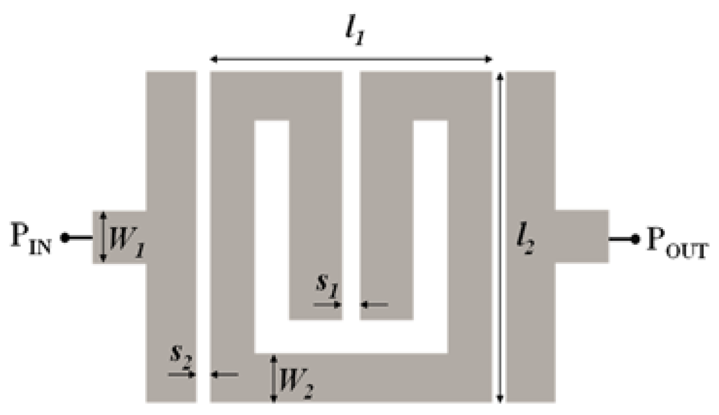
As previously mentioned, near-field chipless RFID systems comprise the reader and the tag. The sensitive part of the reader consists of a microstrip transmission line loaded with a square-shaped split ring resonator (SRR) in bandpass configuration [
57,
58], as can be seen in
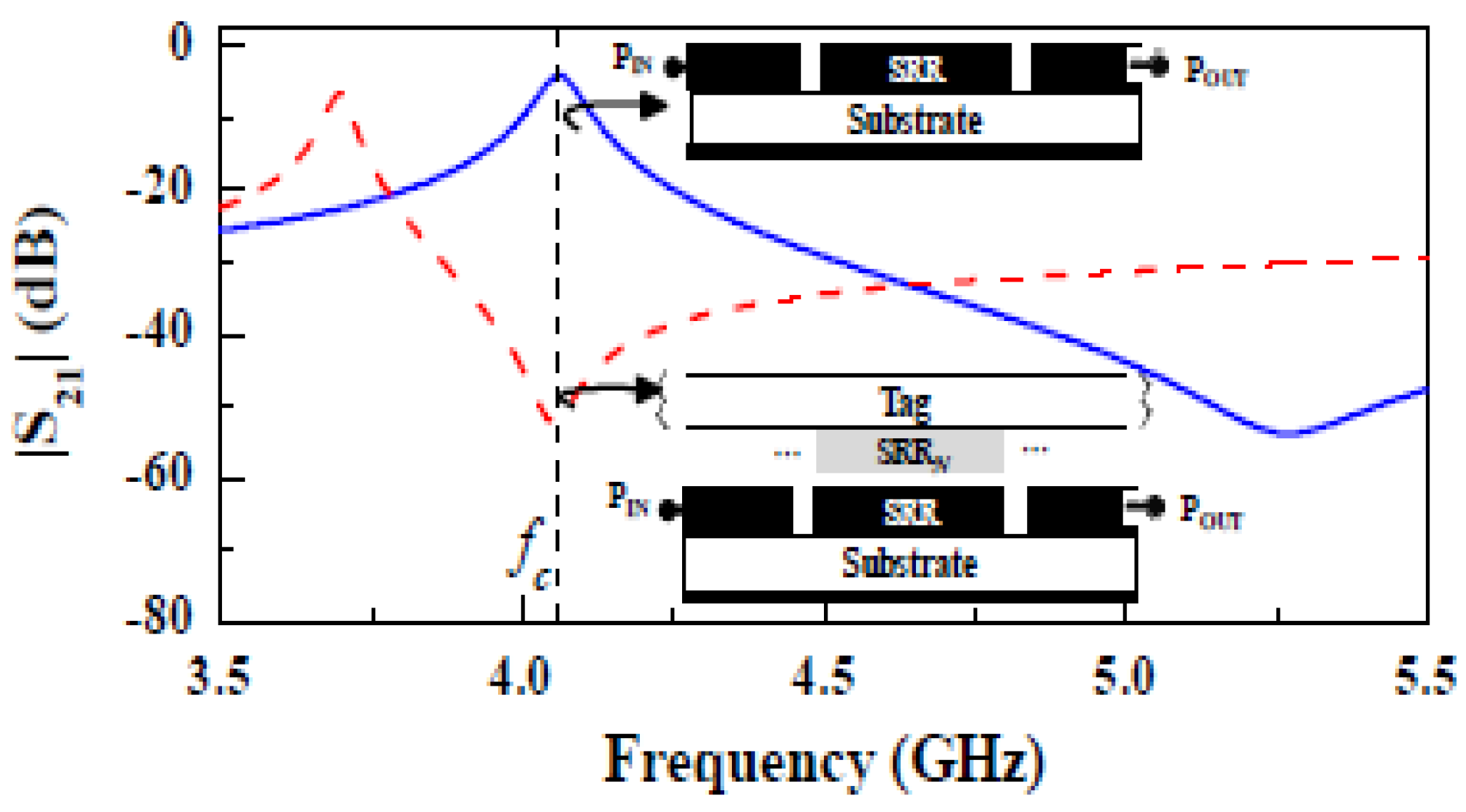
Figure 1. When the tag, consisting of a set of identical resonators to that of the reader but oppositely oriented, is located in close proximity to the sensitive part of the reader, coupling between the resonators arises, and the overall response is shifted down. A large excursion of the transmission coefficient at the design frequency generates a high dynamic range at that frequency, i.e., a high difference between two transmission coefficient values. In
Figure 2, the unloaded reader allows the signal to be transmitted (equal to the ‘1’ logic state); meanwhile, the reader loaded with the tag resonator blocks and reflects back the signal (equals to the ‘0’ logic state). Note that the simulated response depicted in
Figure 2 is a general solution of a tag formed with one resonator element and considering a Rogers substrate with characteristics shown in this figure caption.
3. Materials and Methods
Several works report the development of chipless RFID tags by using metallic inks because of their inherently good electrical conductivity [
60,
61,
62]. More recently, conducting polymers such as poly (3,4-ethylenedioxythiophene) polystyrene sulfonate, hereafter referred to as PEDOT:PSS, have been widely employed in capacitors, transistors and solar cells [
63,
64,
65]. Indeed, PEDOT:PSS possesses interesting features due to its ease of processing, mixed electronics/ionic conductivity and biocompatibility. Using PEDOT:PSS is a challenge since organic conductors usually exhibit conductivities from 2 to 3 times lower than those of metallic inks.
In order to fabricate organic chipless RFID tags, PEDOT:PSS doped with multi-walled carbon nanotubes (named Poly-Ink HC) was purchased from Poly-Ink. In this study, the rheological property of the conductive ink is suitable for drop-on-demand (DoD) inkjet printing given that its viscosity is between 3–8 mPas. The ink was ultrasonically stirred for 1 min and then filtered using a 0.2 µm PVDF filter after which the tags were printed onto a standard DIN A4 photocopy paper using an inkjet printer (Ceradrop CeraPrinter X-Series). The printhead (cartridge) had 16 nozzles each capable of ejecting an ink droplet of 10 pL. As the tag dimensions require a considerable resolution, a single nozzle was selected for droplet ejection for preventing an excess of ink which could produce a short-circuit in S1 and S2 owing to the capillarity of the cellulose. During the inkjet printing process, both the substrate and the cartridge were kept at room temperature. The geometry of the printed resonators of the tags was identical to that of the resonator of the sensitive part of the reader (see
Figure 1). Note that despite the fact that the resonators of the tag were printed on DIN A4 (a different substrate than the resonator of the reader), system functionality is guaranteed. The reason is that the shift in the frequency response (when a resonant element of the tag is on top of the resonator of the reader) is mainly determined by the geometry of such elements, and this is optimum when the geometries of both elements are identical. Nevertheless, it does not mean that the frequency shift does not depend also on the substrate. It does, but a small shift, as in
Figure 2, suffices to differentiate the presence or absence of functional resonant elements in the tag, the principle for tag reading.
Prior to tag fabrication, it was necessary to ensure a proper overlap of the droplets and conductivity. Depending on the selected space between adjacent droplets, a printer can eject isolated drops or produce scalloped, uniform, or bulging lines [
66]. To form a continuous and conducting film, the drop spacing needs to be properly spaced with partial overlap. By carefully optimizing the drop spacing, it is possible to achieve higher resolutions with even edges.
Figure 3a illustrates the printed line topologies across a broad range of drop spacing. As drop spacing is increased above a certain length, the resultant line changes from a scalloped one (for drop spacing 5–10 µm) to a continuous line (drop spacing 20 µm) and then gradually separates into isolated drops (drop spacing over 50 µm). Therefore, the best drop spacing to achieve a uniform pattern is 20 µm since the drop dimension is 42 µm ± 2 µm (
Figure 3a). Once the drop spacing is fixed, an assessment of the conductivity of the printed patterns in the function of the number of layers should be performed. Since the substrate used in this work is based on cellulose, the ink deposited onto it tends to be absorbed through it due to the capillarity. This fact may produce a decrease in the resolution compared with polymeric substrates because the pattern not only stands onto the surface, but also in the cellulose bulk. Hence, this configuration leads to a reduction in the conductivity as the printed pattern comprises both the non-conductive cellulose and the PEDOT:PSS. Therefore, we demonstrated the capability to obtain a conductive pattern onto cellulose without the need to seal and passivate the porosity with a primer.
Figure 3b,c show optical images of inkjet-printed squares printed with one, two, and three layers using a drop spacing of 20 µm. As can be seen, the patterns present sharp edges even with 3 layers, meaning that there is no loss of resolution. Finally,
Figure 3d shows a twenty-bit tag and a zoom of one resonator printed with one, two, and three layers of PEDOT:PSS.
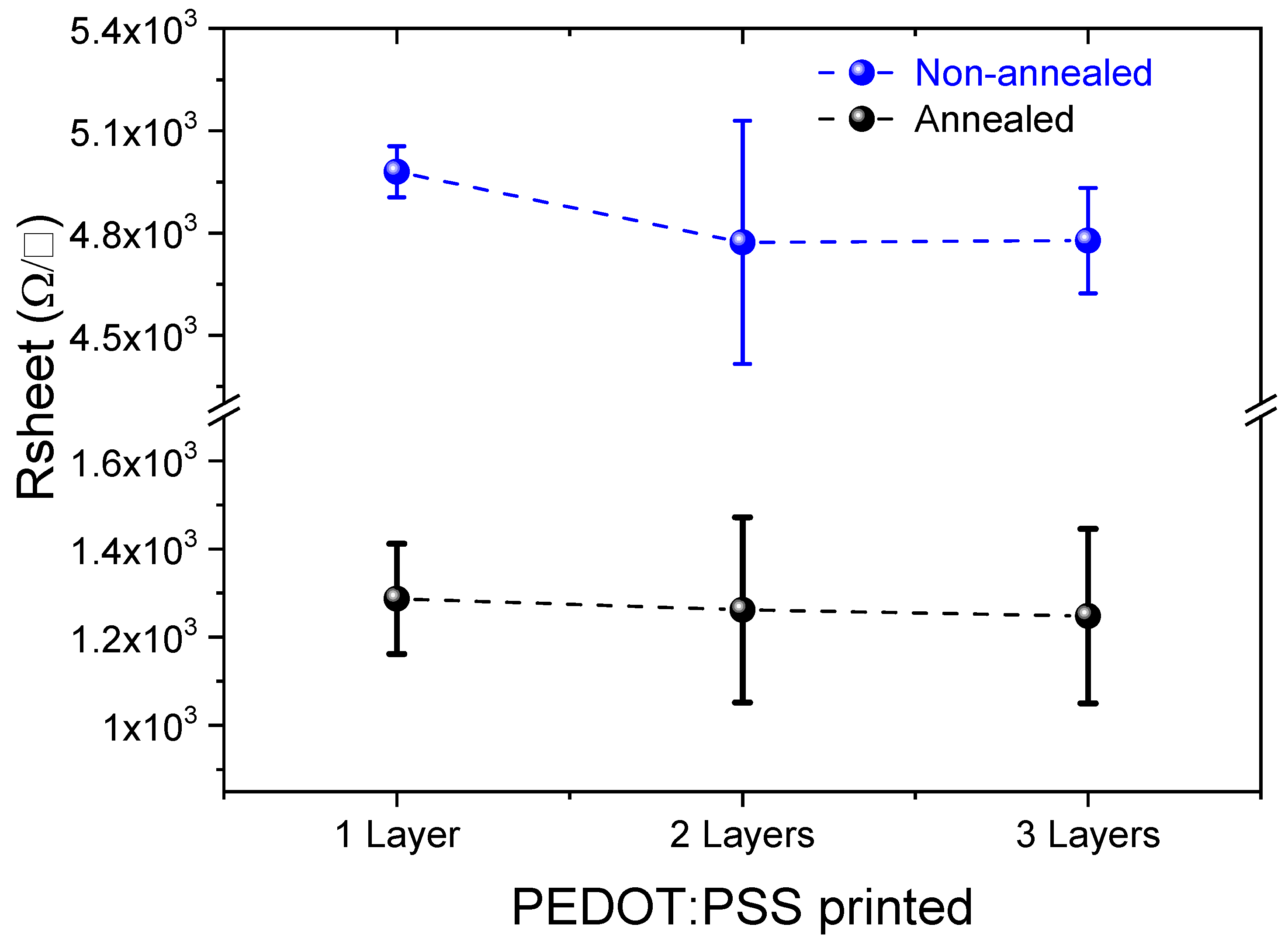
Van der Pauw measurements were carried out (
Figure 4) for one, two, and three layers on paper in order to extract the sheet resistance. The study was conducted both with and without annealing the samples, since the paper is a temperature-sensitive substrate, although this step is used to remove the solvent. The thermal annealing treatment was carried out in the annealed samples by applying 110 °C for 45 min in a conventional oven. A noticeable effect in all the cases was the higher sheet resistance in the range of 10
3 Ω/square compared with the samples printed on polymeric substrates 15–400 Ω/square, because of the penetration of the ink into the cellulose hampering the conductivity. In addition, the increment of the layers contributed to the reduction of the resistance for both annealed and non-annealed samples. The annealing process led to a resistivity sheet resistance of 1.2–1.3 × 10
3 Ω/square, whereas the sheet resistance of the non-annealed samples increased to 4.9–4.7 × 10
3 Ω/square, where the absorption of the solvent was attributed to the cellulose fibers. Despite the higher sheet resistance, the removal of the annealing process brings new opportunities for using cellulose-based substrates while simultaneously producing a substantial reduction in the total cost of the tags. Thus, in our study, the RFID tags were fabricated without annealing.
4. Experimental Tag Validation and Results
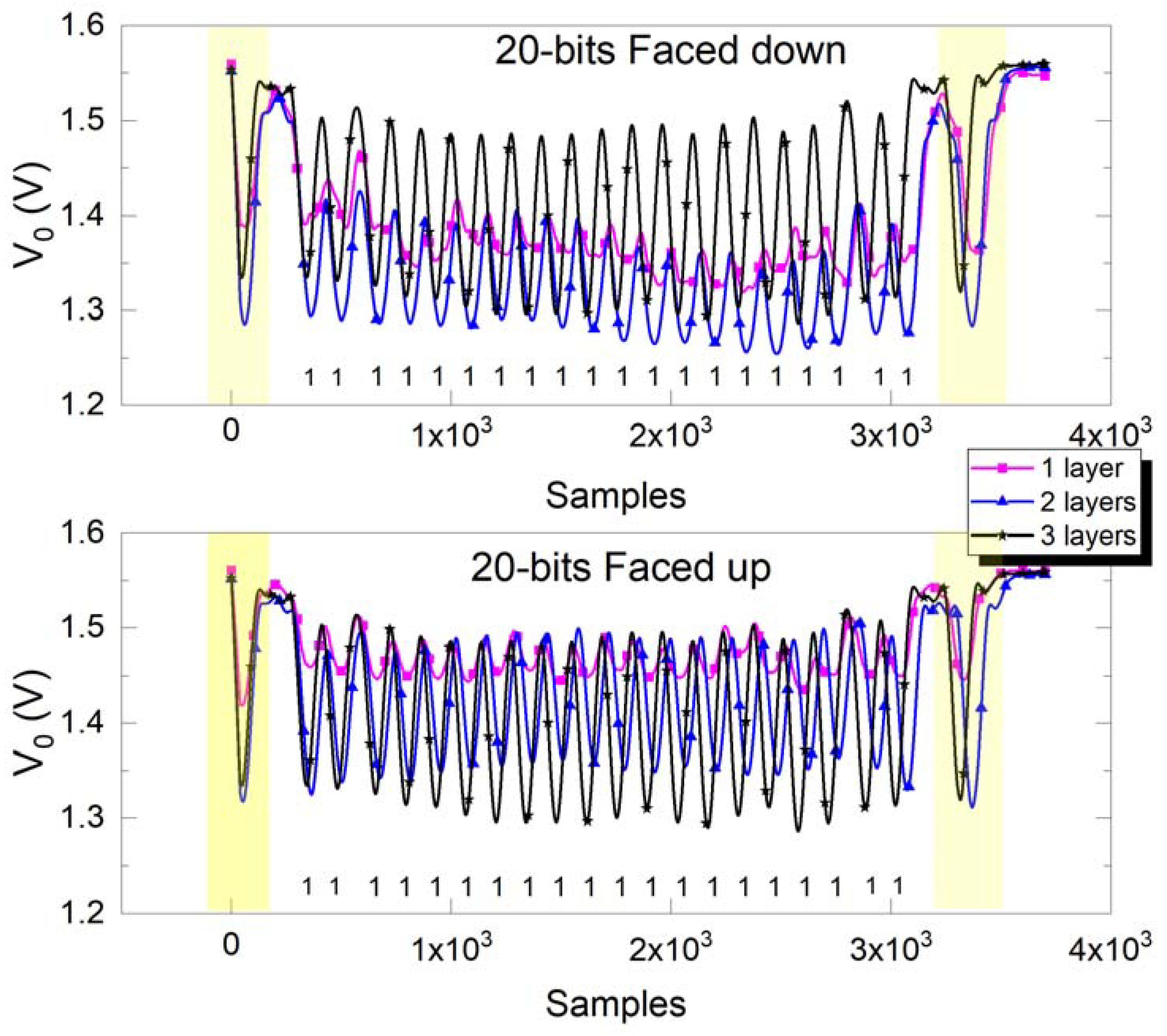
In this section, three different 20-bit tags with all bits set to ‘1’ were fabricated with one, two, and three printed ink layers in order to compare the effect of the resonator ink conductivity on the measured envelope signal. The tags consisted of a linear chain of resonant elements, identical to the one of the reader line. In addition, two trigger bits set to ‘1’ were added at the beginning and at the end of the tag chain in order to know the start and end of the reader system to acquire the data signal. The tags were fabricated by inkjet printing using PEDOT:PSS on ordinary paper substrates (DIN A4). The measured dielectric constant and loss tangent of the paper were εr = 3.11 and tanδ = 0.036 and the measurements were carried out by means of the resonant cavity Agilent 85072A.
The measured envelope functions of the fabricated tags are depicted in
Figure 5. As can be appreciated, the functional resonators (providing the logic state ‘1’) are detected by means of dips in the envelope functions, and tag reading provides the corresponding ID code. However, as the number of printed layers decreases (representing a reduction in the conductivity), the modulation index in the envelope function decreases, and this jeopardizes the detection of the ID code by means of post-processing stages. For example, in the tag printed with one ink layer, it is difficult to obtain the ID code, especially when the tag is read face down. On the contrary, by printing two or three layers, good modulation index for both sides of the tag are obtained, and it suffices to detect the tag code on both faces. Note that the different signal offset levels were obtained as a function of the tag- reading orientation. When the tags are read face up, the envelope signal offsets are in the same level (near to 1,5V). However, when the tags are read face down, they are in a lower level and different for the three tags. This difference is, in part, due to the ink conductivity and the air gap between the tag and the reader [
57].
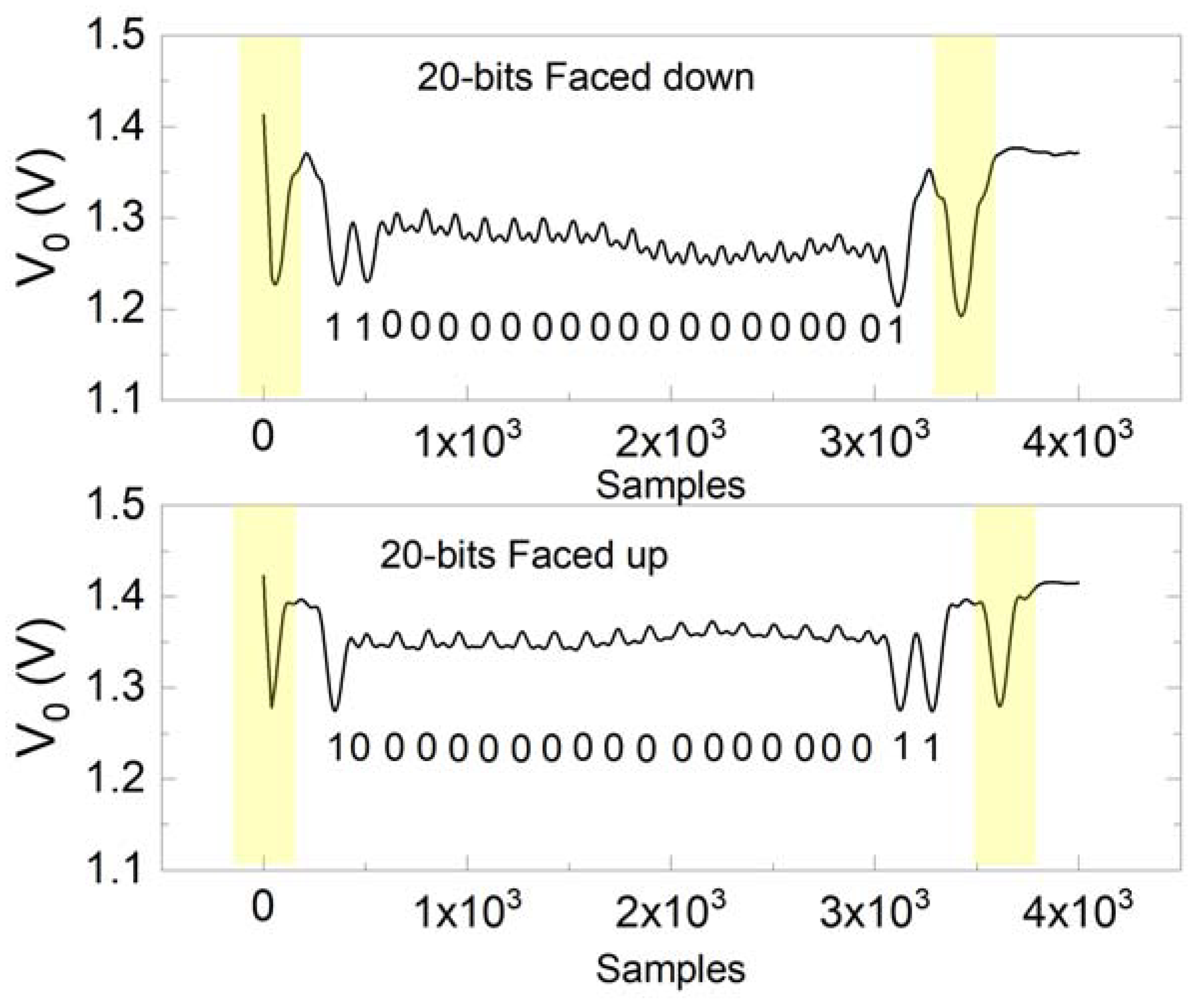
Another example of a 20-bit tag envelope signal is depicted in
Figure 6. In this case, only two layers were printed, and it was enough to detect the ID code clearly. Note that when a bit is set to ‘0’, a very small variation of the envelope signal is observed because of the absence of a certain resonant element at their predefined position (the chain resonator is detuned). With these results, the functionality of the proposed tags, implemented by means of organic inks and printing two layers on ordinary paper substrates, was demonstrated.
The small difference between the face up and face down measured envelope functions allows the addition of a cellulose layer on top of the printed resonators in order to hide them. This approach improves the security of the printed tags because after printing, the resonant elements are buried (sandwiched) in the paper substrate.
5. Tag Re-programmability and Industrial Scaling-Up
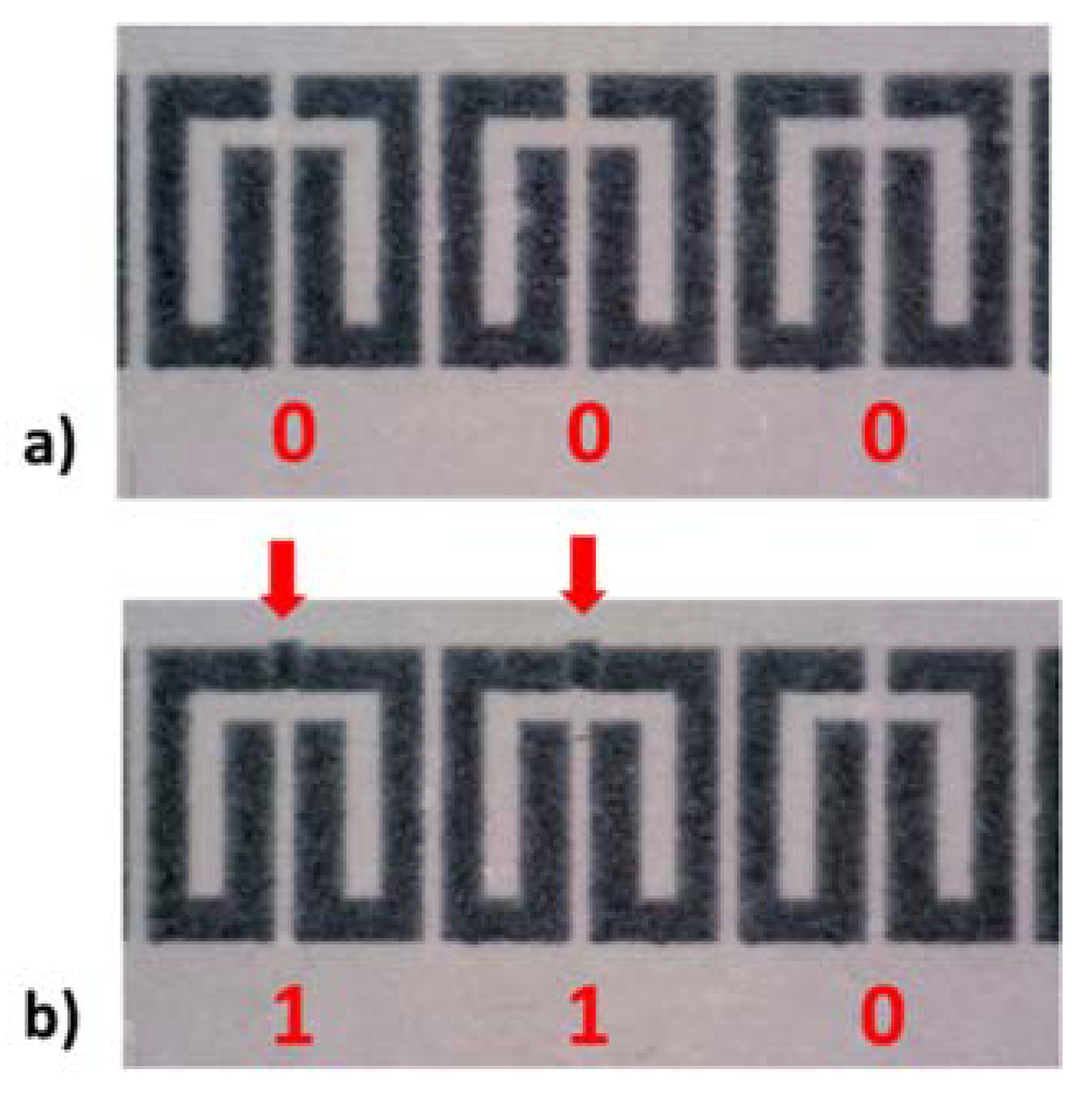
As mentioned before, the tags are linear chains of identical resonators, where each resonator provides a bit of information when it is interrogated by the harmonic signal tuned to the resonance frequency. Such tags can be programmed either by cutting the resonant elements associated with the logic state ‘0’ (making them inoperative as shown in
Figure 7a, or erased, by short-circuiting the cut resonator through inkjet (thus adding conductive ink in order to set the corresponding bit to ‘1’, as shown in
Figure 7b. The main advantage of tag programming/erasing is the possibility of mass-fabrication of all-identical tags, thus reducing fabrication costs. Once fabricated, the tags can be programmed at a later stage, and erased and re-programmed as many times as needed. However, multiple tag programming/erasing cycles may give rise to tag degradation. In typical applications, tags should be programed only once in order to provide a unique ID code after being fabricated (multiple erasing and reprograming is not expected in most applications).
A late-stage codification process can be implemented by additive inkjet printing (selective short-circuits) or laser ablation (physical destruction) procedures to be incorporated to the chipless RFID tag design and into the digital workflow standards already settled in the printing industry. For this purpose, Intense Pulse Light (IPL) post-processing of the printed structures on the millisecond time scale enable single line-scan functionalization of the required area, i.e., selective sintering of the light absorbing structures on the full print layout width, in an R2R compatible manufacturing process, thus bringing a whole different response to the interrogation signal.
Watermarks, serial numbers, holograms, threads, encoding, specific molding, etc., are used to prevent copying and counterfeiting of numerous valuable documents, such as ID cards, banknotes, medical prescriptions, certificates, diplomas, etc., making the list of coding applications for chipless RFID paper enormous.
For security paper applications, the proposed near-field chipless RFID system provides secure and low-cost encoders with unprecedented high data capacity (comparable to that of chipped tags), maintaining recyclability. Data storage resides on the printed tags, not in any further programming step. The tag design and the packaging graphics are printed simultaneously, only resulting in a slight increase in the cost of the package or tag. From the manufacturer’s side, the substrate has no visible change and no further adaption of the production process needs to be implemented. In addition, chipless RFID solutions are printed on the inside, or are hidden below different layers, inaccessible for intentional manipulation.
6. Conclusions
In this paper, we have discussed fundamental aspects of the development of fully recyclable and organic chipless RFID technology mainly focused on the implementation and measurement of tags. These tags can be manufactured using printing processes, such as inkjet printing with organic conductive ink on conventional paper substrates. In addition, a time-domain chipless RFID approach, where the tags are read through near-field coupling (with sequential bit reading) by means of a harmonic interrogation signal, is reported. Validation examples have been discussed and reported, and we have shown that reasonably good results can also be obtained by printing only two ink layers, reducing the manufacturing and sintering time. It has been pointed out that this novel and unconventional system is of special interest in applications involving secure paper, where tag reading by proximity may represent an added value in terms of confidence. In addition, this is a real improvement for an eco-friendly world because the printing processes, such as flexography or inject printing techniques, using organic inks can achieve a lower environmental impact, and the tag unit cost is comparable to that of an optical barcode. This demonstrates the potential of chipless RFID organic technology, which should represent a very good choice for identification applications in the years to come. The adoption of chipless RFID technology opens a new path to low-cost fully printed chipless RFID solutions where the complexity migrates from the tag to the reader, making it possible to break the eurocent cost barrier.
Author Contributions
C.H. and F.P. conceived the reported time-domain chipless RFID approach and designed the active part of the reader and the tags; M.M. developed the electronics necessary for tag reading, carried out the measurements, as well as, analyzed the data; C.M.-D. and R.E. carried out the validation experiments with the inks and printed the tags; M.M. and C.M.-D. wrote the paper; E.R. and F.M. reviewed, edited and supervised the work; L.T. supervised the work; E.R. and F.M conceived the work and they have been the directors of the research. All authors have read and agreed to the published version of the manuscript.
Funding
This work was supported by MICIU-Spain (RTI2018-102070-B-C21), MICIU-Spain (RTC2019-007226-7), Marie Skłodowska-Curie No 801342 (Tecniospring INDUSTRY), Agència per a la Competitivitat de l’Empresa de la Generalitat de Catalunya, by FEDER funds, MICINN-Spain (project PID2019-103904RB-I00), by Generalitat de Catalunya (project 2017SGR-1159), by Institució Catalana de Recerca i Estudis Avançats (who awarded Ferran Martín), and by ERDF funds.
Institutional Review Board Statement
Not applicable.
Informed Consent Statement
Not applicable.
Data Availability Statement
Exclude this statement because do not report any data.
Acknowledgments
The authors would like to thank our R&D partners: Fujifilm Dimatix, Ceradrop and DuPont Teijin for providing us with the research related consumables and their technical details.
Conflicts of Interest
The authors declare no conflict of interest. The founding sponsors had no role in the design of the study, in the collection, analyses, or interpretation of data; in the writing of the manuscript, and in the decision to publish the results.
References
- Martins, R.; Ferreira, I.; Fortunato, E. Electronics with and on paper. Phys. Status Solidi 2011, 5, 332–335. [Google Scholar] [CrossRef]
- Gaspar, D.; Fernandes, S.N.; de Oliveira, A.G.; Fernandes, J.G.; Grey, P.; Pontes, R.V.; Pereira, L.; Martins, R.; Godinho, M.H.; Fortunato, E. Nanocrystalline cellulose applied simultaneously as the gate dielectric and the substrate in flexible field effect transistors. Nanotechnology 2014, 25, 094008. [Google Scholar] [CrossRef] [PubMed]
- Martins, R.F.P.; Ahnood, A.; Correia, N.; Pereira, L.M.N.P.; Barros, R.; Barquinha, P.M.C.B.; Costa, R.; Ferreira, I.M.M.; Nathan, A.; Fortunato, E.E.M.C. Recyclable, flexible, low-power oxide electronics. Adv. Funct. Mater. 2013, 23, 2153–2161. [Google Scholar] [CrossRef]
- Cunha, I.; Barras, R.; Grey, P.; Gaspar, D.; Fortunato, E.; Martins, R.; Pereira, L. Reusable cellulose-based hydrogel sticker film applied as gate dielectric in paper electrolyte-gated transistors. Adv. Funct. Mater. 2017, 27, 1606755. [Google Scholar] [CrossRef]
- Tobjörk, D.; Österbacka, R. Paper electronics. Adv. Mater. 2011, 23, 1935–1961. [Google Scholar] [CrossRef] [PubMed]
- Eder, F.; Klauk, H.; Halik, M.; Zschieschang, U.; Schmid, G.; Dehm, C. Organic electronics on paper. Appl. Phys. Lett. 2004, 84, 2673–2675. [Google Scholar] [CrossRef]
- Hu, L.; Choi, J.W.; Yang, Y.; Jeong, S.; Mantia, F.L.; Cui, L.-F.; Cui, Y. Highly conductive paper for energy-storage devices. Proc. Natl. Acad. Sci. USA 2009, 106, 21490–21494. [Google Scholar] [CrossRef]
- Lessing, J.; Glavan, A.C.; Walker, S.B.; Keplinger, C.; Lewis, J.A.; Whitesides, G.M. Inkjet printing of conductive inks with high lateral resolution on omniphobic “RF paper” for paper-based electronics and MEMS. Adv. Mater. 2014, 26, 4677–4682. [Google Scholar] [CrossRef] [PubMed]
- Magliulo, M.; Mulla, M.Y.; Singh, M.; Macchia, E.; Tiwari, A.; Torsi, L.; Manoli, K. Printable and flexible electronics: From TFTs to bioelectronic devices. J. Mater. Chem. C 2015, 3, 12347–12363. [Google Scholar] [CrossRef]
- Vidor, F.F.; Meyers, T.; Hilleringmann, U. Flexible electronics: Integration processes for organic and inorganic semiconductor-based thin-film transistors. Electronics 2015, 4, 480–506. [Google Scholar] [CrossRef]
- Noh, J.; Jung, M.; Jung, Y.; Yeom, C.; Pyo, M.; Cho, G. Key issues with printed flexible thin film transistors and their application in disposable RF sensors. Proc. IEEE 2015, 103, 554–566. [Google Scholar] [CrossRef]
- Fukuda, K.; Tokito, S. Printed organic thin-film transistors. In Organic Electronics Materials and Devices; Springer: Tokyo, Japan, 2015. [Google Scholar]
- Kahn, B.E. Patterning processes for flexible electronics. Proc. IEEE 2015, 103, 497–517. [Google Scholar] [CrossRef]
- Kang, B.; Lee, W.H.; Cho, K. Recent advances in organic transistor printing processes. ACS Appl. Mater. Interfaces 2013, 5, 2302–2315. [Google Scholar] [CrossRef]
- Choi, C.-H.; Lin, L.-Y.; Cheng, C.-C.; Chang, C. Printed oxide thin film transistors: A mini review. ECS J. Solid State Sci. Technol. 2015, 4, 3044–3051. [Google Scholar] [CrossRef]
- Chung, S.; Jang, M.; Ji, S.B.; Im, H.; Seong, N.; Ha, J.; Kwon, S.K.; Kim, Y.H.; Yang, H.; Hong, Y. Flexible high-performance all-inkjet-printed inverters: Organo-compatible and stable interface engineering. Adv. Mater. 2013, 25, 4773–4777. [Google Scholar] [CrossRef]
- Khan, S.; Lorenzelli, L.; Dahiya, R.S. Technologies for printing sensors and electronics over large flexible substrates: A review. IEEE Sens. J. 2015, 15, 3164–3185. [Google Scholar] [CrossRef]
- Caironi, M.; Noh, Y.-Y. Large Area and Flexible Electronics; Wiley: Weinheim, Germany, 2015. [Google Scholar]
- Joshi, P.C.; Kuruganti, T.; Duty, C.E. Additive Manufacturing: Innovations, Advances, and Applications; Srivatsan, T.S., Sudarshan, T.S., Eds.; CRC Press: Boca Raton, FL, USA, 2016. [Google Scholar]
- Ru, C.; Luo, J.; Xie, S.; Sun, Y. A review of non-contact micro- and nano-printing technologies. J. Micromechanics Microengineering 2014, 24, 5. [Google Scholar] [CrossRef]
- Zheng, Y.; He, Z.; Gao, Y.; Liu, J. Direct desktop printed-circuits-on-paper flexible electronics. Sci. Rep. 2013, 3, srep01786. [Google Scholar] [CrossRef]
- Koga, H.; Nogi, M. Flexible paper electronics. In Organic Electronics Materials and Devices; Ogawa, S., Ed.; Springer: Tokyo, Japan, 2015. [Google Scholar]
- Mansour, A.M.; Shehata, N.; Hamza, B.M.; Rizk, M.R.M. Efficient design of flexible and low cost paper-based inkjet-printed antenna. Int. J. Antennas Propag. 2015, 2015. [Google Scholar] [CrossRef]
- Balde, M.; Jacquemoud-Collet, F.; Vena, A.; Sorli, B. Wet Microelectronic Technologies on Paper Substrate for Flexible Electronic Applications. Sens. Actuators A Phys. 2016, 240, 118–125. [Google Scholar] [CrossRef]
- Yafia, M.; Shukla, S.; Najjaran, H. Fabrication of digital microfluidic devices on flexible paper-based and rigid substrates via screen printing. J. Micromechanics Microengineering 2015, 25, 057001. [Google Scholar] [CrossRef]
- Li, Z.; Liu, H.; Ouyang, C.; Wee, W.H.; Cui, X.; Lu, T.J.; Pingguan-Murphy, B.; Li, F.; Xu, F. Recent advances in pen-based writing electronics and their emerging applications. Adv. Funct. Mater. 2016, 26, 165–180. [Google Scholar] [CrossRef]
- Cooke, M.D.; Wood, D. Fabrication of micron scale metallic structures on photo paper substrates by low temperature photolithography for device applications. J. Micromechanics Microengineering 2015, 25, 115017. [Google Scholar] [CrossRef][Green Version]
- Tai, Y.L.; Yang, Z.G. Fabrication of paper-based conductive patterns for flexible electronics by direct-writing. J. Mater. Chem. 2011, 21, 5938–5943. [Google Scholar] [CrossRef]
- Russo, A.; Ahn, B.Y.; Adams, J.J.; Duoss, E.B.; Bernhard, J.T.; Lewis, J.A. Pen-on-paper flexible electronics. Adv. Mater. 2011, 23, 3426–3430. [Google Scholar] [CrossRef] [PubMed]
- Hyun, W.J.; Secor, E.B.; Rojas, G.A.; Hersam, M.C.; Francis, L.F.; Frisbie, C.D. All-printed, foldable organic thin-film transistors on glassine paper. Adv. Mater. 2015, 27, 7058–7064. [Google Scholar] [CrossRef]
- Chung, S.; Jang, J.; Cho, J.; Lee, C.; Kwon, S.-K.; Hong, Y. All-inkjet-printed organic thin-film transistors with silver gate, source/drain electrodes. Jpn. J. Appl. Phys. 2011, 50, 03CB05. [Google Scholar] [CrossRef]
- Chung, S.; Kim, S.O.; Kwon, S.K.; Lee, C.; Hong, Y. All-inkjet-printed organic thin-film transistor inverter on flexible plastic substrate. IEEE Electron. Device Lett. 2011, 32, 1134–1136. [Google Scholar] [CrossRef]
- Castro, H.F.; Sowade, E.; Rocha, J.G.; Alpuim, P.; Lanceros-Méndez, S.; Baumann, R.R. All-inkjet-printed bottom-gate thin-film transistors using uv curable dielectric for well-defined source-drain electrodes. J. Electron. Mater. 2014, 43, 2631–2636. [Google Scholar] [CrossRef]
- Gomes, H.; Medeiros, M.; Villani, F.; Canudo, J.; Loffredo, F.; Miscioscia, R.; Martínez-Domingo, C.; Ramon, E.; Sowade, E.; Mitra, K.; et al. All-inkjet printed organic transistors: Dielectric surface passivation techniques for improved operational stability and lifetime. Microelectron. Reliab. 2015, 55, 1192–1195. [Google Scholar] [CrossRef]
- Mitra, K.Y.; Sowade, E.; Martínez-Domingo, C.; Ramon, E.; Carrabina, J.; Gomes, H.L.; Baumann, R.R. Potential up-scaling of inkjet-printed devices for logical circuits in flexible electronics. AIP Conf. Proc. 2014, 1646, 106–114. [Google Scholar]
- Sowade, E.; Ramon, E.; Mitra, K.Y.; Martínez-Domingo, C.; Pedro, M.; Pallarès, J.; Loffredo, F.; Villani, F.; Gomes, H.L.; Terés, L.; et al. All-inkjet-printed thin-film transistors: Manufacturing process reliability by root cause analysis. Sci. Rep. 2016, 6, 33490. [Google Scholar] [CrossRef] [PubMed]
- Ko, S.H.; Pan, H.; Grigoropoulos, C.P.; Luscombe, C.K.; Fréchet, J.M.J.; Poulikakos, D. All-inkjet-printed flexible electronics fabrication on a polymer substrate by low-temperature high-resolution selective laser sintering of metal nanoparticles. Nanotechnology 2007, 18, 345202. [Google Scholar] [CrossRef]
- Fukuda, K.; Takeda, Y.; Yoshimura, Y.; Shiwaku, R.; Tran, L.T.; Sekine, T.; Mizukami, M.; Kumaki, D.; Tokito, S. Fully-printed high-performance organic thin-film transistors and circuitry on one-micron-thick polymer films. Nat. Commun. 2014, 5, 4147. [Google Scholar] [CrossRef] [PubMed]
- Vena, A.; Perret, E.; Tedjini, S.; Tourtollet, G.E.P.; Delattre, A.; Garet, F.; Boutant, Y. Design of chipless RFID tags printed on paper by flexography. IEEE Trans. Antennas Propag. 2013, 61, 5868–5877. [Google Scholar] [CrossRef]
- Feng, Y.; Xie, L.; Chen, Q.; Zheng, L.R. Low-cost printed chipless RFID humidity sensor tag for intelligent packaging. IEEE Sens. J. 2015, 15, 3201–3208. [Google Scholar] [CrossRef]
- Finkenzeller, K. RFID Handbook: Fundamentals and Applications in Contactless Smart Cards, Radio Frequency Identification and Near-Field Communication, 3rd ed.; Wiley: Chichester, UK, 2010. [Google Scholar]
- Hunt, V.D.; Puglia, A.; Puglia, M. RFID: A Guide to Radio Frequency Identification; Wiley: Hoboken, NJ, USA, 2007. [Google Scholar]
- Preradovic, S.; Karmakar, N.C. Chipless RFID: Bar code of the future. IEEE Microw. Mag. 2010, 11, 87–97. [Google Scholar] [CrossRef]
- Preradovic, S.; Karmakar, N.C. Multiresonator-Based Chipless RFID: Barcode of the Future; Springer: New York, NY, USA, 2011. [Google Scholar]
- Perret, E. Radio Frequency Identification and Sensors: From RFID to Chipless RFID; Wiley: Hoboken, NJ, USA, 2014. [Google Scholar]
- Rezaiesarlak, R.; Manteghi, M. Chipless RFID: Design Procedure and Detection Techniques; Springer: Berlin, Germany, 2015. [Google Scholar]
- Karmakar, N.C.; Zomorrodi, M.; Divarathne, C. Advanced Chipless RFID: MIMO-Based Imaging 60 GHz-ML Detection; Wiley: Hoboken, NJ, USA, 2016. [Google Scholar]
- Tedjini, S.; Karmakar, N.C.; Perret, E.; Vena, A.; Koswatta, R.; E-Azim, R. Hold the chips: Chipless technology, an alternative technique for RFID. IEEE Microw. Mag. 2013, 14, 56–65. [Google Scholar] [CrossRef]
- Karmaker, N.C. Tag, you’re it radar cross section of chipless RFID tags. IEEE Microw. Mag. 2016, 17, 64–74. [Google Scholar] [CrossRef]
- Dey, S.; Saha, J.K.; Karmakar, N.C. Smart sensing: Chipless RFID solutions for the internet of everything. IEEE Microw. Mag. 2015, 16, 26–39. [Google Scholar] [CrossRef]
- Shao, B.; Chen, Q.; Amin, Y.; Liu, R.; Zheng, L.R. Chipless RFID tags fabricated by fully printing of metallic inks. Ann. Telecommun. 2013, 68, 401–413. [Google Scholar] [CrossRef]
- Vena, A.; Perret, E.; Tedjini, S. Design rules for chipless RFID tags based on multiple scatterers. Ann. Telecommun. 2013, 68, 361–374. [Google Scholar] [CrossRef]
- Forouzandeh, M.; Karmakar, N.C. Chipless RFID tags and sensors: A review on time-domain techniques. Wirel. Power Transf. 2015, 2, 62–77. [Google Scholar] [CrossRef]
- Karmakar, N.C.; Koswatta, R.; Kalansuriya, P.; E-Azim, R. Chipless RFID Reader Architecture; Artech House: Boston, MA, USA, 2013. [Google Scholar]
- Herrojo, C.; Moras, M.; Paredes, F.; Núñez, A.; Ramon, E.; Mata-Contreras, J.; Martín, F. Very low-cost 80-bit chipless-RFID Tags inkjet printed on ordinary paper. Technologies 2018, 6, 52. [Google Scholar] [CrossRef]
- Martin, F.; Herrojo, C.; Mata-Contreras, J.; Paredes, F. Time-Domain Signature Barcodes for Chipless-RFID and Sensing Applications; Springer: Cham, Switzerland, 2020. [Google Scholar]
- Herrojo, C.; Mata-Contreras, J.; Nunez, A.; Paredes, F.; Ramon, E.; Martin, F. Near-field chipless-RFID system with high data capacity for security and authentication applications. IEEE Trans. Microw. Theory Tech. 2017, 65, 5298–5308. [Google Scholar] [CrossRef]
- Herrojo, C.; Mata-Contreras, J.; Paredes, F.; Nunez, A.; Ramon, E.; Martin, F. Near-field chipless-RFID system with erasable/programmable 40-bit tags inkjet printed on paper substrates. IEEE Microw. Wirel. Compon. Lett. 2018, 28, 272–274. [Google Scholar] [CrossRef]
- Herrojo, C.; Paredes, F.; Escudé, R.; Ramon, E.; Martín, F. Near-field chipless-RFID system based on tags implemented with organic inks. In Proceedings of the IEEE Asia-Pacific Microwave Conference (APMC), Singapore, 10–13 December 2019; pp. 108–110. [Google Scholar]
- Singh, R.; Singh, E.; Nalwa, H.S. Inkjet printed nanomaterial based flexible radio frequency identification (RFID) tag sensors for the internet of nano things. RSC Adv. 2017, 7, 48597–48630. [Google Scholar] [CrossRef]
- Zhong, T.; Jin, N.; Yuan, W.; Zhou, C.; Gu, W.; Cui, Z. Printable stretchable silver ink and application to printed RFID tags for wearable electronics. Materials 2019, 12, 3036. [Google Scholar] [CrossRef]
- Gao, B.; Yuen, M.M. Optimization of silver paste printed passive UHF RFID tags. In Proceedings of the IEEE International Conference on Electronic Packaging Technology & High Density Packaging (ICEPT-HDP), Beijing, China, 10–13 August 2009. [Google Scholar]
- Sirringhaus, H.; Kawase, T.; Friend, R.H.; Shimoda, T.; Inbasekaran, M.; Wu, W.; Woo, E.P. High-resolution inkjet printing of all-polymer transistor circuits. Science 2000, 290, 2123–2126. [Google Scholar] [CrossRef]
- Eom, S.H.; Senthilarasu, S.; Uthirakumar, P.; Yoon, S.C.; Lim, J.; Lee, C.; Lim, H.S.; Lee, J.; Lee, S.H. Polymer solar cells based on inkjet-printed PEDOT:PSS layer. Org. Electron. 2009, 10, 536–542. [Google Scholar] [CrossRef]
- Liu, Y.; Cui, T.; Varahramyan, K. All-polymer capacitor fabricated with inkjet printing technique. Solid-State Electron. 2003, 47, 1543–1548. [Google Scholar] [CrossRef]
- Soltman, D.; Subramanian, V. Inkjet-printed line morphologies and temperature control of the coffee ring effect. Langmuir 2008, 24, 2224–2231. [Google Scholar] [CrossRef] [PubMed]
| Publisher’s Note: MDPI stays neutral with regard to jurisdictional claims in published maps and institutional affiliations. |
© 2021 by the authors. Licensee MDPI, Basel, Switzerland. This article is an open access article distributed under the terms and conditions of the Creative Commons Attribution (CC BY) license (https://creativecommons.org/licenses/by/4.0/).
