Article

Silver-Nanowire-Based Localized-Surface-Plasmon-Assisted Transparent Conducting Electrode for High-Efficiency Light-Emitting Diode

1
Korea Photonics Technology Institute (KOPTI), Gwangju 500-460, Korea
2
Department of Photonic Engineering, Chosun University, Gwangju 501-759, Korea
3
Department of Mechanical Engineering, Materials Science and Engineering Program, University of Houston, Houston, TX 77204, USA
4
Advanced Manufacturing Institute (AMI), University of Houston, Houston, TX 77204, USA
5
Texas Center for Superconductivity at UH (TcSUH), University of Houston, Houston, TX 77204, USA
*
Author to whom correspondence should be addressed.
Appl. Sci. 2021, 11(16), 7747; https://doi.org/10.3390/app11167747
Submission received: 30 June 2021 / Revised: 13 August 2021 / Accepted: 20 August 2021 / Published: 23 August 2021
(This article belongs to the Special Issue Light Emitting Diode)

Abstract

:
Silver nanowire (Ag NWs) networks with high transparency and low resistivity are widely used as promising candidates for the replacement of indium tin oxide (ITO)-based transparent conducting oxides (TCOs) in light-emitting diodes (LEDs). However, LEDs with Ag NW electrodes are less efficient than those with ITO electrodes because of their low electrical properties, such as high contact resistance and strong absorption in the visible region. In this work, we tried to improve the efficiency of LEDs with transparent conducting electrodes of Ag NWs networks via localized surface plasmons (LSPs) by adopting silver nanoparticles. We studied the effect of the thickness of the p-GaN layer on surface plasmon coupling. When a 45 nm thick p-GaN layer was used, the internal quantum efficiency was improved by LSP coupling between a dipole of QW and Ag NW/NP, and the light extraction was improved because the NPs afforded a leakage mode and acted as scattering centers.

1. Introduction

Transparent conducting electrodes (TCEs) are widely used in optoelectronic devices such as light-emitting diodes (LEDs), solar cells, liquid crystal displays, and touch screens. Owing to increasing demand for these products, significant research is being conducted to enhance their performance by manufacturing process optimization. Among many candidate materials, indium tin oxide (ITO) is generally used in many applications. However, ITO has drawbacks, such as having a high cost, unsatisfactory light transmission, chemical instability, and a weak ion barrier effect [1,2]. In addition, ITO exhibits strong absorption in the ultraviolet (UV)/blue spectral range [3]. Therefore, it is necessary to find more suitable materials to applicate transparent electrode. Metal nanowires (NWs) such as silver NWs and carbon nanotubes have been studied as promising candidates for replacing ITO in optoelectronic devices [3,4,5,6,7,8,9,10,11,12,13,14]. Among them, Ag NWs are especially promising because of their high conductivity (σAg = 6.3 × 10⁷ S m−1) compared to other metals commonly used as electrode materials for LEDs [15]. In addition, Ag is well known as a good material for obtaining surface plasmon (SP) resonance with a GaN LED, which increases the IQE and LEE [16,17,18,19,20]. Our group recently demonstrated the near-UV LEDs with high-quality solution-processed Ag NW TCEs with sheet resistances of 30–40 Ω/sq and optical transmittances of over 85% to replace ITO-based TCEs [3]. This fabrication process is quite simple and relatively inexpensive, like that for ITO-based TCEs, suggesting that Ag NWs are promising candidate materials for use in next-generation TCEs in LEDs. However, many groups have only focused on replacing ITO-based TCEs with Ag-NW-based TCEs [3,4,5,6,7,8,9,10,11,12]. By contrast, to enhance the properties of Ag-NW-based TCEs, our group recently reported TCEs based on Ag NWs and nanoparticles (NPs) in which localized surface plasmons (LSPs) are excited; consequently, the internal quantum efficiency (IQE) is improved by dipoles of quantum well (QW) and SP coupling of Ag metal, and the light extraction efficiency (LEE) is improved by NPs working as a leakage mode and act as scattering centers [16]. However, the optimal structure for adopting the Ag-NW/NP-based TCE in III-nitride LEDs is still unknown.
In this work, we studied the improvement of the efficiency of LEDs with Ag-NW/NP-based TCEs. In addition, the use of Ag NWs and NPs also increases the IQE and LEE [14]. To improve the efficiency of LEDs with the Ag-NW/NP-based TCE, we attempted to control the spacing between NW and NP and the thickness of the p-GaN layer between the TCE and QWs. When a 45 nm thick p-GaN layer and 35 nm NPs at a high density of 8 × 1010 cm−2 were used, the efficiency of the LED was significantly improved, owing to the phenomena described above.

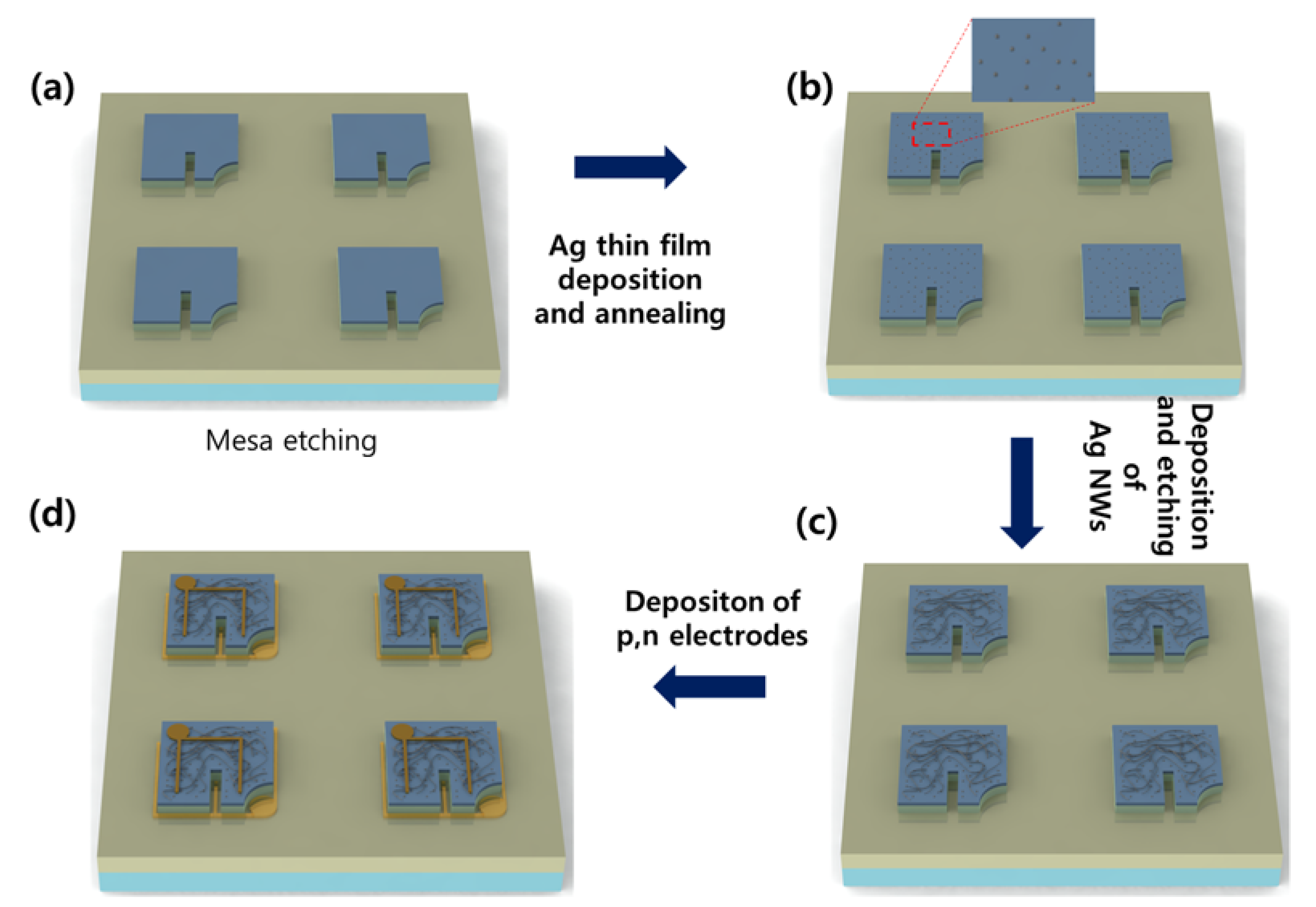
2. Experimental Section

InGaN-based blue LEDs with a dominant emission peak of 450 nm were grown on sapphire substrates using metal–organic chemical vapor deposition. The LEDs consisted of a 4 µm thick n-GaN layer (Si = 1 × 1019 cm−3), a seven period multiple-QW (MQW) active layer consisting of undoped InGaN QWs (3 nm) and undoped GaN barriers (7 nm), and a p-GaN layer. The SP fringing field penetration depth for metal film into the dielectric materials such as GaN was given by Z = λ/2π[(εGaNεmetal)/εGaN2]1/2, where εGaN and εmetal are the dielectric constants of GaN and Ag, respectively [16].
The penetration depth was calculated as ~45 nm for coupling between the dipole of QW and SP of Ag at 2.75 eV for the blue emission. We first attempted to identify a mechanism for improving the LED efficiency by using an SP-enhanced TCE based on Ag NWs. For that, we used an LED with a 45 nm thick p-GaN layer to study the improvement in the IQE due to QW–LSP coupling, whereas we used an LED with a 120 nm thick p-GaN layer to study the increase in LEE due to LSP–TM light coupling without QW–SP coupling. The 45 nm thick p-GaN consisted of 15 nm (magnesium (Mg) = 3 × 1019 cm−3), 15 nm (Mg = 1 × 1018 cm−3), and 15 nm (Mg = 1 × 1020 cm−3) layers, whereas the 120 nm thick p-GaN consisted of 15 nm (Mg = 3 × 1019 cm−3), 90 nm (Mg = 1 × 1018 cm−3), and 15 nm (Mg = 1 × 1020 cm−3) layers, respectively. Then, to improve the LEE by increasing the light output by QW–SP coupling, we combined NPs with the NWs, where the NPs afford a leakage mode and act as scattering centers.
Figure 1 shows a schematic diagram of blue LEDs with the Ag-NW/NP-based TCE.

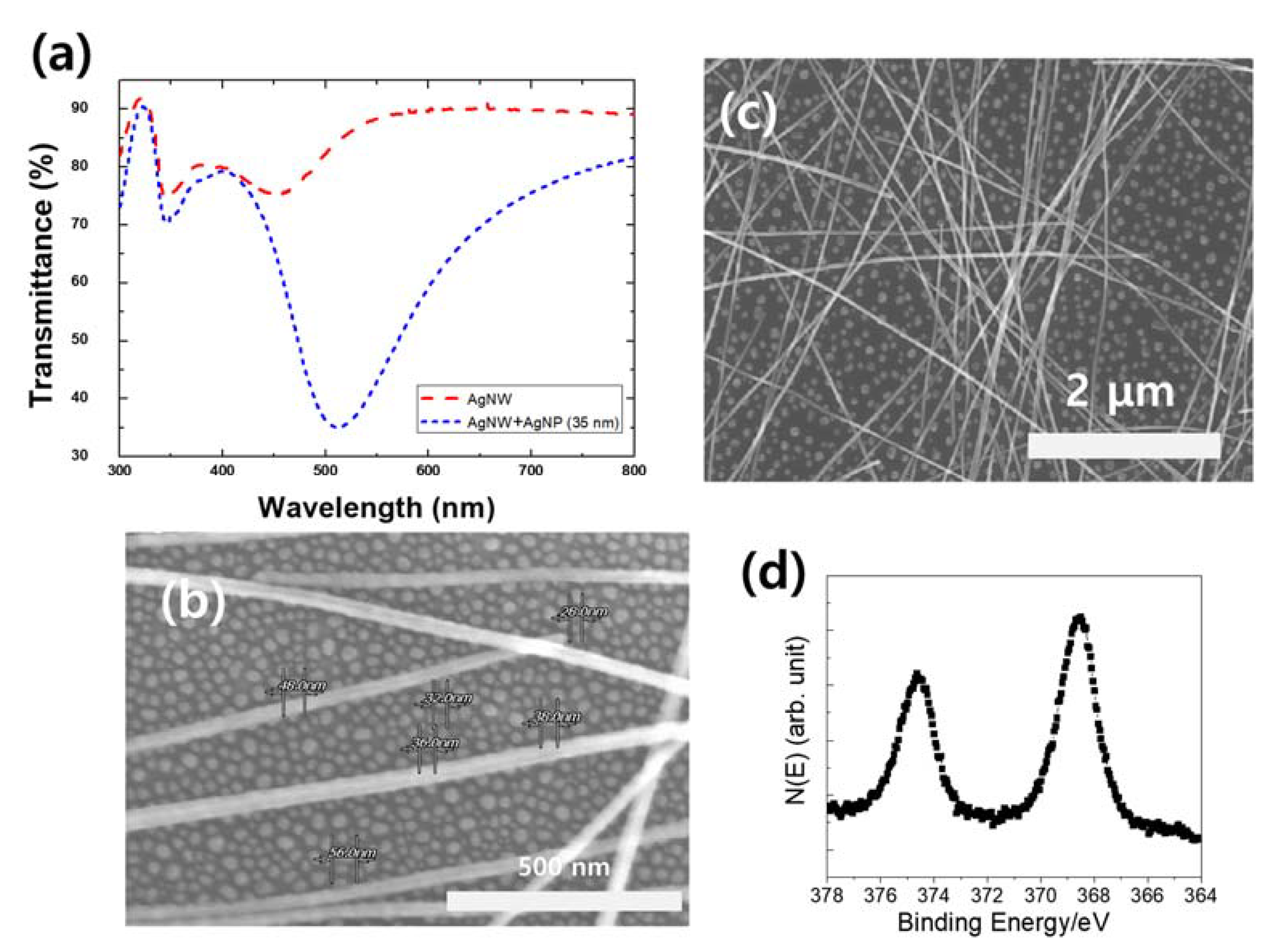
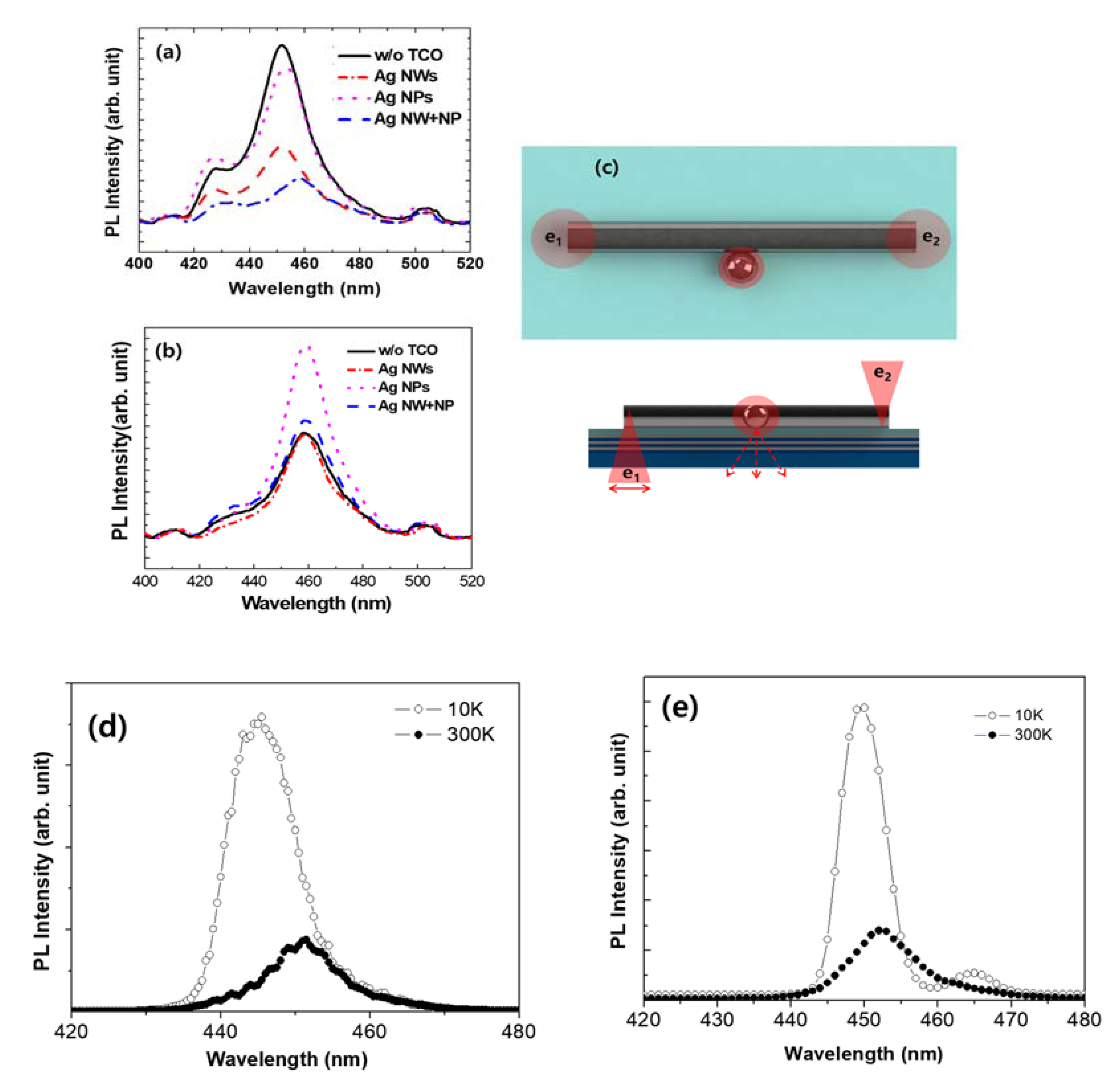
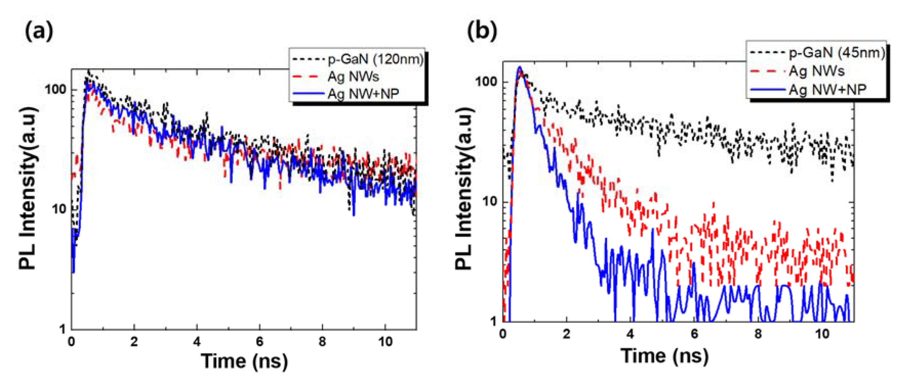
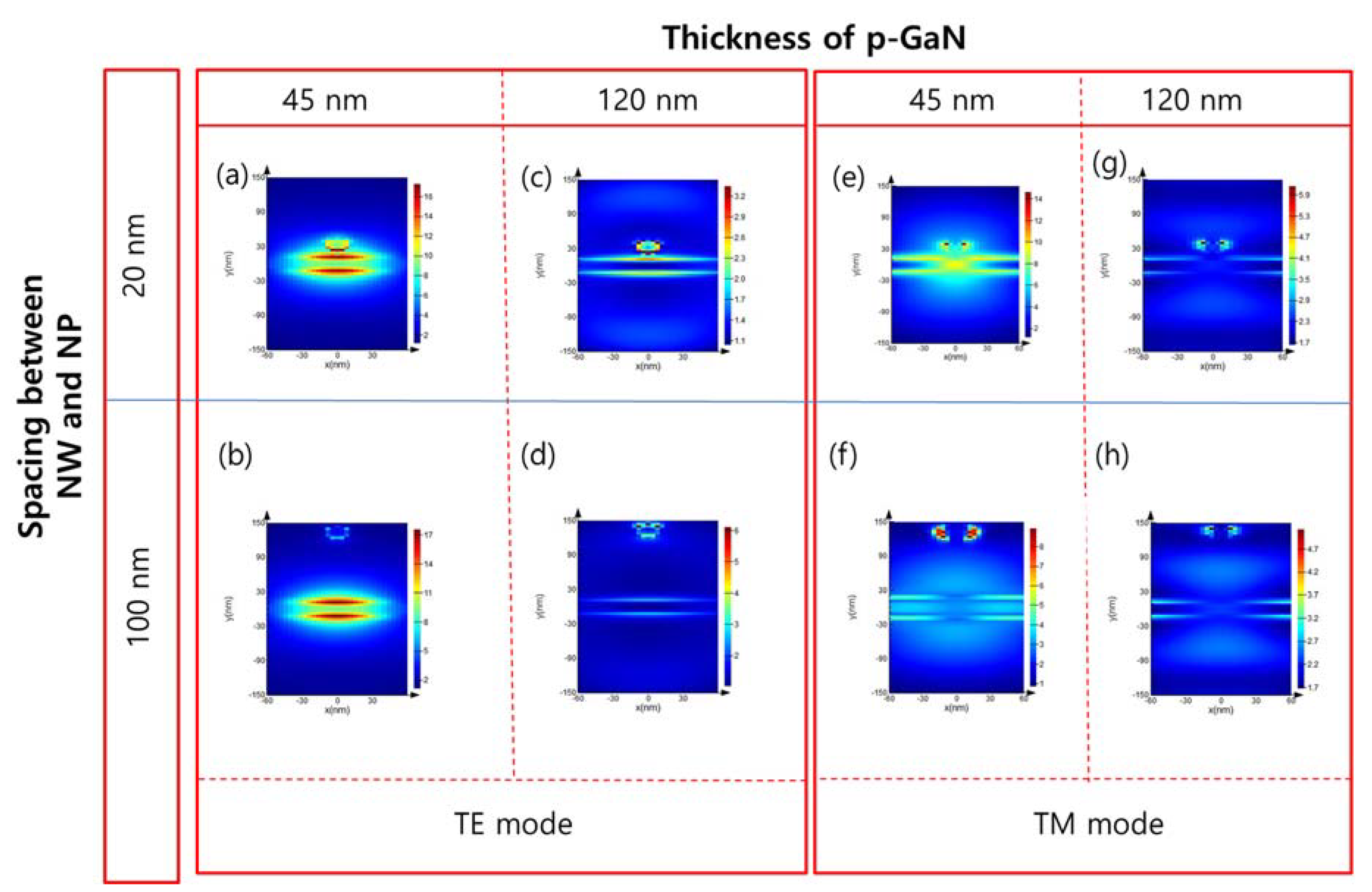
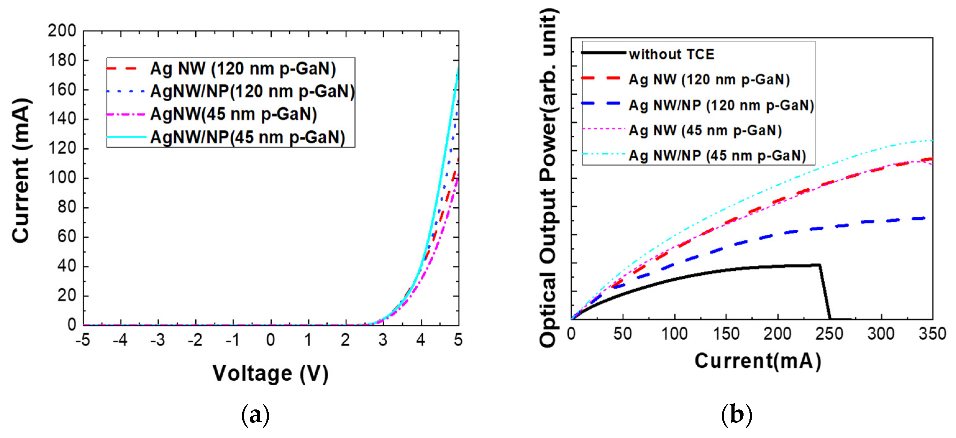
3. Results and Discussion

Figure 2 shows field-emission scanning electron microscopy (FE-SEM) images of Ag NP/NW TCEs with NP sizes and the transmittance of Ag NW and Ag NP/NW TCEs. To form Ag NW TCEs with high conductivity, we used Ag NWs that were 35 nm in diameter and 25 μm in length [3,16]. The sheet resistance of the 200 nm thick Ag NWs and Ag NW/NP TCEs was measured as 30 ± 5 Ω/sq. The contact resistance did not change after NPs were added to the TCE. The contact resistance between the TCE with Ag NWs and p-GaN is 2.5 × 10⁻³ Ω cm2. This is sufficient to form an Ohmic contact on p-GaN [3].
To obtain the leakage mode and scattering centers, we fabricated Ag NPs with sizes of 35 ± 13 nm, as shown in Figure 2b,c, respectively. The density of the Ag NPs with a size of 35 ± 13 nm was 8 × 1010 cm−2. We found that the transmittance of the Ag NWs exceeded 90% in the visible region. When the NPs were added, the TCE exhibited strong absorption that corresponds to SP resonance. This result may be caused by the enhancement of localized surface plasmon resonance by Ag NPs [21,22,23]. The oxidation of Ag affected the electrical properties of the LED and the SP effect. To confirm that Ag NW and NP was not oxidized, we performed X-ray photoelectron spectroscopy, as shown in Figure 2d. Figure 1d shows that the Ag3d5/2 peak was 368.3 eV. This indicated Ag NP and NW were not oxidized [24].
To determine the optimal structure for improving the efficiency of LEDs with Ag NW or Ag NW/NP TCEs, the enhancement mechanism first had to be identified. Considering that the penetration depth was estimated as ~45 nm for QW–SP coupling at an emission energy of 2.75 eV in the blue LED, the Ag NW or Ag NW/NP TCE was deposited on 45 nm thick p-GaN for coupling between dipoles of QW and LSP of Ag NW/NP. To study the effect of LSP–transverse magnetic (TM) or LSP–transverse electric (TE) light coupling on the LEE in the absence of QW–LSP coupling, the Ag NP, Ag NW, or Ag NW/NP TCE was deposited on a 120 nm thick p-GaN layer. Figure 3a shows the photoluminescence (PL) spectra of InGaN/GaN MQW LEDs with Ag NW, Ag NP, or Ag NW/NP TCEs and 45 nm or 120 nm thick p-GaN layers. QW–SP coupling cannot be expected in the LEDs with a 120 nm thick p-GaN layer. Thus, the efficiency of the LED may be improved by the extraction of TE and TM light. However, when we used NPs alone, the PL intensity decreased. This result indicates that the increase in LEE due to LSP–TM/TE light coupling does not compensate for the absorption of photons in Ag NWs or NPs. However, when the NWs were combined with NPs, the PL intensity was 30% higher than that obtained using Ag NWs alone. This result shows that NPs can improve the LEE for TE/TM polarization.
The PL intensity of LEDs with a Ag NW TCE and 45-nm-thick p-GaN layer is similar to that of the LEDs without a TCE, whereas that of LEDs with a Ag NW/NP TCE is higher than that of the LEDs without TCEs, as shown in Figure 3b. Because the p-GaN layer is 45 nm thick, QW–SP coupling is possible, and the IQE is improved. When the dipole energies in the InGaN QWs and the SP energy of the Ag are similar, the exciton dipole energies excited in the QWs is transferred to the SP modes of the Ag.
The nanostructure and roughness of the Ag layer allows SPs with high momentum to scatter. Then, they lose their momentum, and become coupled to the radiated light. This process occurs much more rapidly than the radiative recombination of exciton dipoles in the InGaN QWs [16], and thus the PL intensity of QW can be improved. Although the PL intensity was significantly higher when only Ag NPs were used owing to increases in the IQE and LEE, Ag NPs alone cannot be used as the TCE. In addition, we found that the PL intensity did not increase when we used TCEs with only Ag NWs. Ag NWs can act as waveguides in nanoscale regions to localize the electromagnetic energy arising from the hybrid nature of SP polaritons (SPPs), which are electromagnetic (EM) waves. EM waves coupled to charge oscillations at the Ag–GaN interface and SPP waves can be optically excited at the distal ends of the NW. However, the intensity of the excited light decreases significantly with increasing propagation distance [25]. Because 20 μm long NWs were used to obtain TCEs with good electrical properties, many electromagnetic waves were absorbed during propagation in the NWs. Therefore, the higher PL intensity exhibited by the LED with the Ag NW TCE cannot be attributed to photon absorption in SPPs. When Ag NPs were used with Ag NWs, the PL intensity increased by 20%.
The SPPs propagate along to interface between the NW and GaN with a momentum higher than the free-space wavelength used for dipole excitation. The momentum of SPPs propagated along to interface between the NW and GaN must be removed from the surface-bound SPP wave to convert the SPPs back to photons at a desired location. NPs close to Ag NWs act as a radiative center to overcome this momentum mismatch and facilitate the momentum of SPPs to free-space photons [25,26]. In addition, all Ag NPs can work as scattering centers because the nanostructure of the Ag layer allows the scattering of SPs with high momentum, as described above. Therefore, the increased PL intensity of the LED with a Ag NW/NP TCE can be attributed to the increase in light extraction at the NW/NP junction and the increase in scattering by Ag NPs, as shown in Figure 3c. Emission can be excited at both ends of the NW by propagation at the interface between the p-GaN layer and TCE.
To assume the improvement of IQE by Ag NW/NP TCE, we tried to measure temperature-dependent photoluminescence with a 25 mW 325 nm He-Cd laser. By comparting the ratio of the integrated PL intensity between 300 K and 0 K, it was possible to find the increase in IQE [27]. The ratio of PL intensities (I300K/I10K) of LED without TEC and with Ag NW/NP TCE were 27.2% and 34.8%, respectively. Based on this result, we found that the IQE can be increased by 30% with Ag NW/NP compared to that of IQW without TCE, shown in Figure 3d,e. This result indicated that the improvement of PL intensity can be attributed to the increase in IQE by SP + QW coupling without the quenching of light extraction.
To elucidate the light outcoupling effects of metal layer, three-dimensional finite-difference time-domain (FDTD) simulations were studied, and the results were compared with the experimental results, as shown in Figure 4. The LED structures with the Ag NW/NP TCE were used in the FDTD simulation. To understand the effects of the geometric configuration on QW–SP coupling in the LEDs, a numerical calculation was performed based on a genetic algorithm by setting a periodic boundary condition. In this investigation, pulse emission sources with TE and TM polarization were used by propagating light to the slab representing the LED. As shown in Figure 4, light propagates along the interface between GaN and Ag NW, and the PL is significantly enhanced by LSP–QW coupling when the thickness of the p-GaN layer is 45 nm. In addition, many photons with TE and TM polarization are radiated by the leakage mode at the NW–NP junction, as shown in Figure 4a,c,e,g. These results indicated that the enhanced PL intensity afforded by the Ag NW/NP TCE can be attributed to an enhancement in the leakage and scattering rate by Ag NPs in LSP–QW coupling. However, when the distance between the Ag NWs and NPs is large, the light extraction is not significantly improved, as shown in Figure 4b,d,f,g. From FDTD simulation, in Ag-NW-based TCE, NP can act as a light scattering point to improve the extraction of photons. So, to improve the light extraction, it is desirable to increase the of density of NPs.
Figure 5a,b show the time-resolved PL spectra of the LEDs without TCEs and with Ag NW and Ag NW/NP TCEs for p-GaN thicknesses of 120 and 45 nm at the temperature of room temperature (300 K), respectively. As expected, the penetration of SP–QW coupling was observed only in the samples with a 45 nm thick p-GaN layer, and there was no change in decay time in the LEDs with a 120 nm thick p-GaN layer. However, the decay time decreased significantly in the LEDs with Ag NW TCEs and Ag NW/NP TCEs when the p-GaN thickness was 45 nm. In Figure 5, all decay curves were fitted with an exponential decay model. In the LED with a 45 nm thick p-GaN layer, the calculated decay times were 10, 1, and 0.5 ns for LEDs without a TCE, with the Ag NW TCE, and with the Ag NW/NP TCE, respectively. The Purcell effect is defined as the ratio of the classical radiated power to the dipole of the cavity to the dipole emission power of the bulk material, thus predicting the rate of spontaneous emission of an LED [28]. The Purcell factor is be calculated numerically using a commercial grade finite-difference time-domain (FDTD) simulation with suggested method by M. Nami et. al. The Purcell factor of LED with Ag NW/NP TCE was calculated to 37 at 465 nm. This value is reasonable in QW-SP-coupled LEDs to improve the spontaneous emission [29]. Therefore, the spontaneous rate of LED with Ag NW/NP-based TCEs can be increased by strong coupling between the QWs and TCE.
The current–voltage (I–V) characteristics and the optical output power of a blue LED without TCEs, with Ag NW, and with Ag NW/NP TCEs were studied. We found that the electrical properties of LEDs is improved by adopting Ag NP in both LED with 45 nm and 120 nm thick p-GaN, as shown in Figure 6a. This result can be attributed to the improvement of the Ohmic behavior with atomic inter-diffusion during the thermal annealing process to form NP [30]. As shown in Figure 6b, the output power of LEDs with 120 nm thick p-GaN are decreased with Ag NW or Ag NW/NP TCE. This result can be attributed to light absorption by the metal nanostructrure. However, the optical output power of LEDs with 45 nm thick p-GaN is slightly improved by Ag NW/NP-based TCEs. These results are consistent with the PL measurements and simulation results. A large enhancement in the optical output power of the LED is expected if the size, uniformity and density of Ag NW/NPs are optimized.

4. Conclusions

We demonstrated localized-surface-plasmon-assisted transparent conducting silver-nanowire networks for high-efficiency light-emitting diodes. We found that by combining Ag NP with a NW network, the efficiency of LED is significantly improved by an increase in IQE by coupling between the dipole of QW and the LSP of NW/NP and light extraction by an increase in the leakage and scattering rate by NPs.

Author Contributions

Conceptualization and methodology: J.-Y.K. and M.-K.K.; investigation: G.-G.O., E.K., H.-S.K. and G.H.; formal analysis: J.-Y.K., J.-H.R. and M.-K.K.; writing—original draft: M.-K.K.; writing—review and editing: M.-K.K. All authors have read and agreed to the published version of the manuscript.

Funding

This work was supported by the Human Resources Program in Energy Technology of the Korea Institute of Energy Technology Evaluation and Planning (KETEP) through financial resources from the Ministry of Trade, Industry and Energy, Republic of Korea (Grant No. 20194030202410) and by a 2018 grant from the research fund of Chosun University.

Institutional Review Board Statement

Not applicable.

Informed Consent Statement

Not applicable.

Data Availability Statement

Not applicable.

Conflicts of Interest

The authors declare no conflict of interest.

References

  1. Sharma, S.; Shriwastava, S.; Kumar, S.; Bhatt, K.; Charu Tripathi, C. Alternative transparent conducting electrode materials for flexible optoelectronic devices. Opt. Rev. 2018, 26, 223. [Google Scholar] [CrossRef]
  2. Kuo, C.; Chang, S.J.; Su, Y.K.; Chuang, R.; Chang, C.; Wu, L.; Lai, W.; Chen, J.F.; Sheu, J.; Lo, H. Nitride-based near-ultraviolet LEDs with an ITO transparent contact. Mater. Sci. Eng. B 2004, 106, 69–72. [Google Scholar] [CrossRef]
  3. Kim, J.Y.; Jeon, J.H.; Kwon, M.K. Indium tin oxide-free transparent conductive electrode for GaN-based ultraviolet light-emitting diodes. ACS Appl. Mater. Inter. 2015, 7, 7945–7950. [Google Scholar] [CrossRef]
  4. Lee, K.; Shin, J.W.; Park, J.H.; Lee, J.; Joo, C.W.; Lee, J.I.; Cho, D.H.; Lim, J.T.; Oh, M.C.; Ju, B.K. A light scattering layer for internal light extraction of organic light-emitting diodes based on silver nanowires. ACS Appl. Mater. Inter. 2016, 8, 17409–17415. [Google Scholar] [CrossRef]
  5. Guo, H.; Lin, N.; Chen, Y.; Wang, Z.; Xie, Q.; Zheng, T.; Gao, N.; Li, S.; Kang, J.; Cai, D. Copper nanowires as fully transparent conductive electrodes. Sci. Rep. 2013, 3, 2323. [Google Scholar] [CrossRef] [PubMed] [Green Version]
  6. Jo, G.; Choe, M.; Cho, C.Y.; Kim, J.H.; Park, W.; Lee, S.; Hong, W.K.; Kim, T.W.; Park, S.J.; Hong, B.H. Large-scale patterned multi-layer graphene films as transparent conducting electrodes for GaN light-emitting diodes. Nanotechnology 2010, 21, 175201. [Google Scholar] [CrossRef] [PubMed] [Green Version]
  7. Seo, T.H.; Kim, B.K.; Shin, G.; Lee, C.; Kim, M.J.; Kim, H.; Suh, E.K. Graphene-silver nanowire hybrid structure as a transparent and current spreading electrode in ultraviolet light emitting diodes. Appl. Phys. Lett. 2013, 103, 51105. [Google Scholar]
  8. Jeong, G.J.; Lee, J.H.; Han, S.H.; Jin, W.Y.; Kang, J.W.; Lee, S.N. Silver nanowires for transparent conductive electrode to GaN-based light-emitting diodes. Appl. Phys. Lett. 2015, 106, 31118. [Google Scholar] [CrossRef]
  9. Zhu, R.; Chung, C.H.; Cha, K.C.; Yang, W.; Zheng, Y.B.; Zhou, H.; Song, T.B.; Chen, C.C.; Weiss, P.S.; Li, G. Fused silver nanowires with metal oxide nanoparticles and organic polymers for highly transparent conductors. ACS Nano 2011, 5, 9877–9882. [Google Scholar] [CrossRef] [PubMed]
  10. Yu, Z.; Zhang, Q.; Li, L.; Chen, Q.; Niu, X.; Liu, J.; Pei, Q. Highly flexible silver nanowire electrodes for shape-memory polymer light-emitting diodes. Adv. Mater. 2011, 23, 664–668. [Google Scholar] [CrossRef]
  11. Oh, M.; Jin, W.Y.; Jeong, H.J.; Jeong, M.S.; Kang, J.W.; Kim, H. Silver nanowire transparent conductive electrodes for high-efficiency III-nitride light-emitting diodes. Sci. Rep. 2015, 5, 13483. [Google Scholar] [CrossRef] [Green Version]
  12. Park, J.S.; Kim, J.H.; Kim, J.Y.; Kim, D.H.; Na, J.Y.; Kim, S.K.; Kang, D.; Seong, T.Y. Formation of an indium tin oxide nanodot/Ag nanowire electrode as a current spreader for near ultraviolet AlGaN-based light-emitting diodes. Nanotechnology 2016, 28, 45205. [Google Scholar] [CrossRef]
  13. Song, W.; Fan, X.; Xu, B.; Yan, F.; Cui, H.; Wei, Q.; Peng, R.; Hong, L.; Huang, J.; Ge, Z. All-Solution-Processed Metal-Oxide-Free Flexible Organic Solar Cells with Over 10% Efficiency. Adv. Mater. 2018, 26, 1800075. [Google Scholar] [CrossRef]
  14. Xu, X.; Lin, S.; Li, Q.; Zhang, Z.; Lvanov, I.N.; Li, Y.; Wang, W.; Gu, B.; Zhang, Z.; Hsuech, C.; et al. Optical Control of Fluorescence through Plasmonic Eigenmode Extinction. Sci. Rep. 2015, 5, 1. [Google Scholar] [CrossRef] [PubMed] [Green Version]
  15. Kim, J.Y.; Na, S.I.; Ha, G.Y.; Kwon, M.K.; Park, I.K.; Lim, J.H.; Park, S.J.; Kim, M.H.; Choi, D.; Min, K. Thermally stable and highly reflective AgAl alloy for enhancing light extraction efficiency in GaN light-emitting diodes. Appl. Phys. Lett. 2006, 88, 43507. [Google Scholar] [CrossRef]
  16. Kim, J.Y.; Cho, Y.H.; Chung, T.H.; Jang, Y.J.; Kim, H.; Bang, S.; Leec, A.; Jeong, M.S.; Ryou, J.H.; Kwon, M.K. Localized surface plasmon-enhanced transparent conducting electrode for high-efficiency light emitting diode. Mater. Lett. 2020, 271, 127790. [Google Scholar] [CrossRef]
  17. Kwon, M.K.; Kim, J.Y.; Kim, B.H.; Park, I.K.; Cho, C.Y.; Byeon, C.C.; Park, S.J. Surface-plasmon-enhanced light-emitting diodes. Adv. Mater. 2008, 20, 1253–1257. [Google Scholar] [CrossRef]
  18. Okamoto, K.; Niki, I.; Shvartser, A.; Narukawa, Y.; Mukai, T.; Scherer, A. Surface-plasmon-enhanced light emitters based on InGaN quantum wells. Nat. Mater. 2004, 3, 601–605. [Google Scholar] [CrossRef]
  19. Cho, C.Y.; Hong, S.H.; Park, S.J. Improvement of optical and electrical properties of indium tin oxide layer of GaN-based light-emitting diode by surface plasmon in silver nanoparticles. Thin Sol. Film. 2015, 590, 76–79. [Google Scholar] [CrossRef]
  20. Chuang, S.H.; Tsung, C.S.; Chen, C.H.; Ou, S.L.; Horng, R.H.; Lin, C.Y.; Wuu, D.S. Transparent conductive oxide films embedded with plasmonic nanostructure for light-emitting diode applications. ACS Appl. Mater. Inter. 2015, 7, 2546–2553. [Google Scholar] [CrossRef]
  21. Hu, L.; Kim, H.S.; Lee, J.Y.; Peumans, P.; Cui, Y. Scalable coating and properties of transparent, flexible, silver nanowire electrodes. ACS Nano 2010, 4, 2955–2963. [Google Scholar] [CrossRef]
  22. Kapoor, S. Preparation, Characterization, and Surface Modification of Silver Particles. Langmuir 1998, 14, 1021. [Google Scholar] [CrossRef]
  23. Biteen, J.S.; Lewis, N.S.; Atwater, H.A.; Mertens, H.; Polman, A. Spectral tuning of plasmon-enhanced silicon quantum dot luminescence. Appl. Phys. Lett. 2006, 88, 131109. [Google Scholar] [CrossRef] [Green Version]
  24. Gao, X.; Wang, S.; Li, W.J.; Zheng, Y.; Zhang, R.; Zhou, P.; Yang, Y.; Chen, L. Study of structure and optical properties of silver oxide films by ellipsometry, XRD and XPS methods. Thin Sol. Film. 2004, 455, 438. [Google Scholar] [CrossRef]
  25. Singh, D.; Dasgupta, A.; Aswathy, V.; Tripathi, R.P.; Kumar, G.P. Directional out-coupling of light from a plasmonic nanowire-nanoparticle junction. Opt. Lett. 2015, 40, 1006–1009. [Google Scholar] [CrossRef] [PubMed] [Green Version]
  26. Song, M.; Bouhelier, A.; Bramant, P.; Sharma, J.; Dujardin, E.; Zhang, D.; Colas-des-Francs, G. Imaging Symmetry-Selected Corner Plasmon Modes in Penta-Twinned Crystalline Ag Nanowires. ACS Nano 2011, 5, 5874. [Google Scholar] [CrossRef] [PubMed]
  27. Lu, T.; Ma, Z.; Du, C.; Fang, Y.; Wu, H.; Jiang, Y.; Wnag, L.; Dai, L.; Jia, H.; Liu, W. Temperature-dependent photoluminescence in light-emitting diodes. Sci. Rep. 2014, 4, 6131. [Google Scholar] [CrossRef] [PubMed] [Green Version]
  28. Nami, M. Feezell, D. Optical properties of Ag-coated GaN/InGaN axial and core-shell nanowire light-emitting diodes. J. Opt. 2015, 17, 25004. [Google Scholar] [CrossRef] [Green Version]
  29. Zhu, S.; Yu, Z.; Liu, L.; Yang, C.; Cao, H.; Xi, X.; Zhao, L. Enhancing the spontaneous emission rate by modulating carrier distribution in GaN-based surface plasmon light-emitting diodes. Opt. Expr. 2017, 25, 9617. [Google Scholar] [CrossRef]
  30. Oh, M.; Kim, H. High-efficiency GaN-based light-emitting diodes fabricated with identical Ag contact formed on both n- and p-layers. Opt. Expr. 2013, 21, 20857. [Google Scholar] [CrossRef]
Figure 1. Schematic illustrations and images corresponding to steps for the fabrication of GaN LEDs with Ag-NW/NP-based TCE. (a) To fabricate LEDs 500 × 500 µm2 in size, the p-GaN and MQWs were sequentially etched using inductively coupled plasma with boron trichloride gas until n-contact layer was exposed. (b) Ag films with thicknesses of 1 nm were selectively deposited by e-beam evaporation on the p-GaN and annealed at 500 °C for 1 min in nitrogen ambient to form Ag NPs. (c) Ag NWs were chemically synthesized according to a previously reported method [19], dispersed in deionized water, and deposited by spin-coating method to obtain a flat film. After photolithography to form TCE region, the Ag NWs were etched using a dilute diluted nitric acid solution of HNO3/H2O (10:1). For a comparative study, a Ag NW layer without NPs was deposited. To form an Ohmic contact, the coated Ag NW layers were annealed at 150 °C for 10 min in nitrogen ambient. (d) Cr/Au was deposited on TCE and n-GaN by e-beam evaporation to obtain n- and p-pads.
Applsci 11 07747 g001
Figure 2. (a) Transmittance of Ag NW and Ag NW/NP TCEs for different NP sizes. FE-SEM images of Ag NW/NP TCEs with NP size with (b) 2 μm scale bar and (c) 500 nm scale bar, (d) XPS spectrum of Ag NW/NP TCE.
Applsci 11 07747 g002
Figure 3. PL spectra of GaN LEDs with (a) 120 nm thick and (b) 45 nm thick p-GaN layer without TCE and with Ag NW, Ag NP, and Ag NW/NP TCEs and (c) schematic diagram of light extraction by plasmon leakage radiation and PL spectra with GaN LED (45 nm thick p-GaN layer) (d) without TCE and (e) with Ag NW/NP TCE at 10 K and 300 K.
Applsci 11 07747 g003
Figure 4. FDTD simulation of Ag NW/NP TCEs using sapcing between the Ag NW and Ag NP of 20 nm with (a) 45 nm and (c) 120 nm-thick p-GaN for TE mode and (e) 45 nm and (g) 120 nm-thick p-GaN for TM mode. That of of Ag NW/NP TCEs using sapcing between the Ag NW and Ag NP of 100 nm with (b) 45 nm and (d) 120 nm-thick p-GaN for TE mode and (f) 45 nm and (h) 120 nm-thick p-GaN for TM mode.
Applsci 11 07747 g004
Figure 5. Time-resolved PL spectra of blue LEDs without TCE and with and without Ag NPs with (a) 120 nm thick and (b) 45 nm thick p-GaN layer.
Applsci 11 07747 g005
Figure 6. (a) Current–voltage characteristic and (b) optical output power of LED with Ag NW and NW/NP TCEs.
Applsci 11 07747 g006
Publisher’s Note: MDPI stays neutral with regard to jurisdictional claims in published maps and institutional affiliations.

