Article

Design and Experiment of Electronically Tunable Voltage-Mode Biquad and Output Current Amplitude Oscillator

1
Department of Electronic Engineering, National Chin-Yi University of Technology, Taiping, Taichung 41170, Taiwan
2
Department of Electronic Engineering, Ming Chi University of Technology, Taishan, New Taipei 24301, Taiwan
3
Department of Electrical Engineering, California State University Fullerton, Fullerton, CA 92831, USA
*
Author to whom correspondence should be addressed.
Appl. Sci. 2021, 11(16), 7357; https://doi.org/10.3390/app11167357
Submission received: 12 July 2021 / Revised: 8 August 2021 / Accepted: 9 August 2021 / Published: 10 August 2021
(This article belongs to the Special Issue Selected Papers from IMETI 2021)

Abstract

:
This study presents an electronically tunable configuration for the design of a voltage-mode (VM) biquad with four input terminals and three output terminals. The proposed circuit employs four operational transconductance amplifiers (OTAs) and two grounded capacitors. Depending on the selections of the four input voltage signals, all the standard filtering functions can be realized. The proposed configuration simultaneously provides VM inverting band-pass, non-inverting low-pass, and non-inverting band-reject filtering functions without any component-matching choices. It offers the features of a resistorless structure, high-input impedance, electronic control of the pole frequency and quality factor, and low active and passive sensitivities. The measured power dissipation of the biquad is 0.96 W under 32 mA constant output current. The measured 1 dB power gain compression point of the output inverting band-pass filter is −7 dBm. The measured value of the third-order intercept point is 5.136 dBm, and the measured value of the third-order intermodulation distortion is −50.83 dBc. Moreover, the measured value of the spurious-free dynamic range is 53.49 dB, and the figure-of-merit of the biquad is 268.75 × 10³. In addition, an electronically controllable quadrature oscillator (QO) with amplitude of output current can be realized using the proposed biquad. The proposed electronically controllable QO can provide an amplitude modulation signal or an amplitude shift keying signal, and is widely applied in signal processing systems and electronic communication systems. PSpice simulations and experimental results are accomplished.

1. Introduction

With increasing emphasis on voltage-mode (VM) biquads and oscillators, there is still a need to develop active components for VM biquads and oscillators. Oscillators [1,2,3,4,5,6] and biquads [7,8,9,10,11,12,13,14] are the most crucial circuit blocks in numerous applications, such as electronic communications, signal processing systems, and measurement systems. Especially in communication modulation systems, the sinusoidal oscillator is utilized to generate the carrier signals for amplitude modulation (AM) and amplitude shift keying (ASK) modulation. Most VM continuous-time biquad designs require the following features: (a) Achievement of five generic filtering signals, that is, low-pass filter (LPF), band-pass filter (BPF), high-pass filter (HPF), band-reject filter (BRF), and all-pass filter (APF) responses. (b) Utilization of grounded capacitors, which is attractive for absorbing shunt parasitic capacitance of the active component and suitable for integrated circuit (IC) implementation. (c) High-input impedance, which is suitable for easy cascading in VM operation without needing any extra voltage followers. (d) Orthogonal tunability of resonance angular frequency (ωo) and quality factor (Q). (e) Low ωo and Q sensitivities with respect to the active and passive components. On the other hand, most quadrature oscillator (QO) designs require the following features: realization of two quadrature sinusoidal voltage outputs with 90° phase difference, independent control of frequency of oscillation (FO) and condition of oscillation (CO), electronic controllability, employment of grounded capacitors, and so on. However, the electronically controllable QO with amplitude of output current should also be considered. The amplitude of output current can be electronically adjusted by fine-tuning the direct-current (DC) bias current (IB), which is suitable for signal processing systems and AM/ASK systems.
The VM electronically tunable, high-input impedance configurations used in the design of operational transconductance amplifier and capacitor (OTA-C) biquads are worthy of study, because they are suitable for the cascade in VM operation and the fine-tuning of the deviation of conventional electronic components. OTA provides highly linear electronic controllability and has a wide tunable range of transconductance gain (gm), which is an attractive feature for circuit designers [15,16,17,18,19,20,21,22,23]. OTAs are commercially available ICs, and LT1228 from Linear Technology Corporation [24] has been widely used to implement OTA-based circuits. The transconductance of LT1228 is electronically controlled by an external DC bias current IB. The OTA-C biquad does not require a resistor, so it is very suitable for IC compared to other conventional active elements. Recently, some types of electronically tunable VM OTA-based biquads have been developed [25,26,27,28,29,30]. The circuits in [25,26] employ six OTAs, but the proposed circuits cannot simultaneously realize LPF, inverting BPF (IBPF) and BRF responses from the same structure. In 2019, three interesting VM electronically tunable OTA-C biquads were proposed, which employ five OTAs along with two grounded capacitors [27,28,29]. The circuit proposed in [27] cannot use the same structure to realize LPF, IBPF, and BRF responses. The circuits proposed in [28,29] can realize LPF, IBPF, and BRF responses with the same configuration, and can be simply converted to QO. However, none of the circuits proposed in [25,26,27,28,29] can be transformed into an electronically controllable QO with high-output impedance and amplitude-controllable sinusoidal current output signal. In 2020, another VM biquad using one dual-output OTA (DO-OTA), three OTAs, and two grounded capacitors was proposed [30]. The proposed circuit can realize LPF, IBPF, and BRF responses with the same configuration, and can be simply transferred to QO. However, the proposed circuit cannot electronically control the amplitude of the high-output impedance sinusoidal current signal. The amplitude of electronically controlled high-output impedance sinusoidal current signals can be applied in AM/ASK systems.
In this study, a new electronically tunable VM biquad with four inputs and three outputs is presented. The biquad has the following advantages: (i) using one DO-OTA, three OTAs, two grounded capacitors, and resistorless realization, which is suitable for integration, (ii) simultaneously realizing LPF, IBPF, and BRF responses without changing the circuit structure, (iii) realizing all the standard biquad functions from the same circuit structure, (iv) high-input impedance, (v) orthogonal electronic-tuning the characteristic parameters of ωo and Q, (vi) easily transformed into a QO with high-output impedance and amplitude-controllable sinusoidal current output signal, and (vii) easily realizing AM/ASK of the oscillator. Table 1 summarizes the performance comparison between the proposed biquad and the previously reported biquads [25,26,27,28,29,30]. Regarding the OTA-based circuits proposed in [25,26,27,28,29,30], the proposed circuit has electronically controllable amplitude of sinusoidal current output with high-output impedance and can be used in an AM/ASK systems. Table 2 compares the additional performance of the proposed biquad and the previously reported biquads [25,26,27,28,29,30].

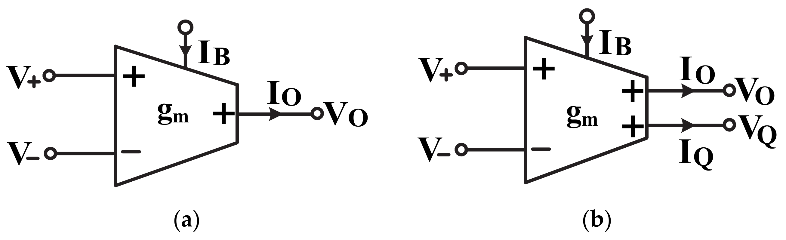
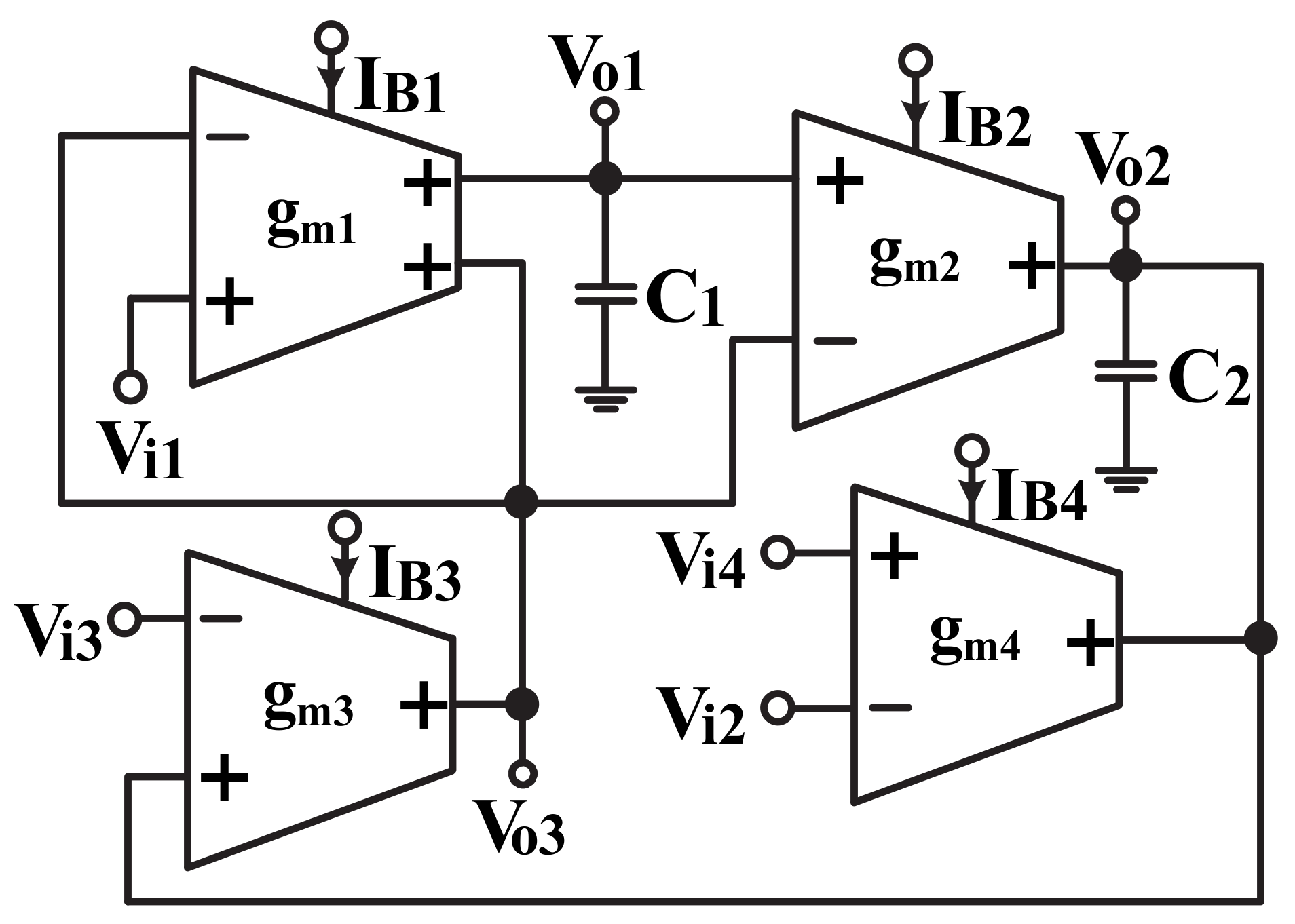
2. Proposed Electronically Tunable VM OTA-C Biquad

OTA offers a high linear electronic controllability and its transconductance gain has a wide tunable range [19]. The electrical symbol of the OTA is shown in Figure 1. According to Figure 1, the single-ended output OTA consists of an input differential pair, an output current mirror, and a gm control unit. The output current of a single-ended OTA is characterized by IO = gm(V+ − V−), where V+ and V− are the input signals applied to the non-inverting and inverting terminals, respectively [19]. The gm value is electrically controllable by an external DC bias current IB, which leads electronic controllability to the design biquad or oscillator parameters. The DO-OTA has two identical current outputs, which can be described by IO = IQ = gm(V+ − V−). Figure 2 shows the proposed biquad with four inputs and three outputs. It is configured by only one DO-OTA, three OTAs, and two grounded capacitors. Routine analysis of the proposed electronically controllable OTA-C biquad in Figure 2 yielded the following three-output voltage signals.
V o 1 = 1 D ( s ) [ g m 1 g m 2 g m 3 V i 1 + g m 1 g m 3 g m 4 ( V i 2 V i 4 ) + sC 2 g m 1 g m 3 V i 3 ]
V o 2 = 1 D ( s ) [ sC 1 g m 1 g m 2 V i 1 sC 1 g m 1 g m 4 ( V i 2 V i 4 ) + ( sC 1 g m 2 g m 3 + g m 1 g m 2 g m 3 ) V i 3 ]
V o 3 = 1 D ( s ) [ ( s 2 C 1 C 2 g m 1 + g m 1 g m 2 g m 3 ) V i 1 sC 1 g m 3 g m 4 ( V i 2 V i 4 ) s 2 C 1 C 2 g m 3 V i 3 ]
where the denominator D(s) is:
D ( s ) = s 2 C 1 C 2 g m 1 + sC 1 g m 2 g m 3 + g m 1 g m 2 g m 3
From Equations (1)–(4), the VM transfer functions can be obtained according to input and output conditions as follows:
Part I: If only Vi1 is applied to the input voltage signal, Vin, the output voltage functions Vo1, Vo2, and Vo3 can be simultaneously obtained, as shown in Equations (5)–(7):
V o 1 V in = g m 1 g m 2 g m 3 D ( s )
V o 2 V in = sC 1 g m 1 g m 2 D ( s )
V o 3 V in = s 2 C 1 C 2 g m 1 + g m 1 g m 2 g m 3 D ( s )
Equations (5)–(7) show that the LPF, IBPF, and BRF signals can be simultaneously implemented.
Part II: According to Equation (3), the proposed biquad can realize six different generic filtering signals. Assuming that gm1 = gm3 and gm2 = gm4 = kgm3, where k is the scale factor, Equation (3) can be rewritten as:
V o 3 = ( s 2 + 1 τ 1 τ 2 ) V i 1 s k τ 2 ( V i 2 V i 4 ) s 2 V i 3 s 2 + s k τ 2 + 1 τ 1 τ 2
where in Equation (8), τ1 = (C1/gm2) and τ2 = (C2/gm3) are the realized time-constants. Examining Equation (8) shows that the LPF, BPF, IBPF, inverting HPF (IHPF), BRF, and APF signals can be implemented by appropriately applying the input signals without the need for an inverting-type input signal. According to Equation (8), the following six different generic filtering signals can be obtained as:
(1)
LPF: Vi2 = Vi4 = 0 and Vi1 = Vi3 = Vin.
(2)
BPF: Vi1 = Vi2 = Vi3 = 0 and Vi4 = Vin.
(3)
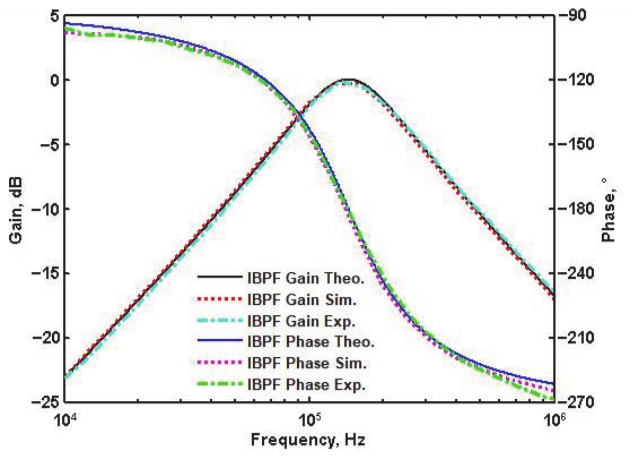
IBPF: Vi1 = Vi3 = Vi4 = 0 and Vi2 = Vin.
(4)
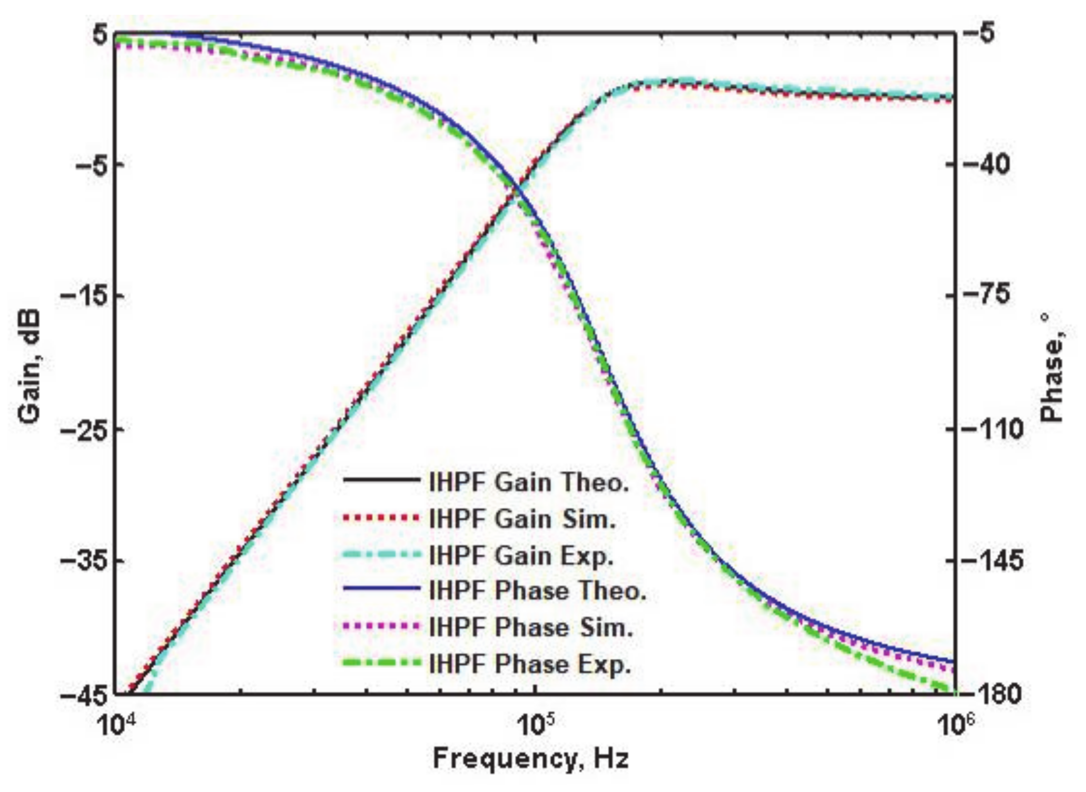
IHPF: Vi1 = Vi2 = Vi4 = 0 and Vi3 = Vin.
(5)
BRF: Vi2 = Vi3 = Vi4 = 0 and Vi1 = Vin.
(6)
APF: Vi3 = Vi4 = 0 and Vi1 = Vi2 = Vin.
From Parts I and II, the biquad structure can be applied as a single-input and three-output VM multifunction biquad, and the LPF, IBPF, and BRF functions from the three output terminals can be realized without any component-matching conditions. It can also be applied as a four-input and single-output VM universal biquad, and can realize six different generic filtering signals in the same structure. The characteristic parameters ωo and Q of the biquad can be calculated as:
ω o = g m 2 g m 3   C 1 C 2 ,   Q = g m 1 C 2 C 1 g m 2 g m 3

3. Proposed Electronically Tunable VM QO with Amplitude of Output Current

The biquad in Figure 2 can be used as the proposed QO with output current amplitude, when Vi1 and Vi2 are connected to the ground while Vi3 and Vi4 are connected to Vo1 and Vo2, respectively. The current output terminal of gm4 in Figure 2 can be the AM/ASK modulated current output terminal, as shown in Figure 3. The characteristic equation of the electronically controllable OTA-C QO with amplitude of output current can be obtained as in Equation (10).
s 2 C 1 C 2 g m 1 + s ( C 1 g m 2 C 2 g m 1 ) g m 3 + g m 1 g m 2 g m 3 = 0
Thus, CO and FO of the electronically controllable OTA-C QO are as follows:
CO :   C 1 g m 2 C 2 g m 1
FO :   f o = 1 2 π g m 2 g m 3   C 1 C 2
From Equations (11) and (12), CO can be controlled independently from FO by varying gm1, and FO can be controlled by gm3. Hence, the proposed QO in Figure 3 has independent electronic control of CO and FO. The two output voltages, Vo1 and Vo3, of the proposed QO can be expressed as:
V o 1 V o 3 = g m 1 sC 1
For sinusoidal steady state, Equation (13) becomes:
V o 1 V o 3 = g m 1 ω o C 1 e j 90 °
Based on Equation (14), the proposed QO has two sinusoidal signal voltages with 90° phase difference. Furthermore, the output current IAM/ASK can be obtained as:
I AM / ASK = g m 4 V o 2
The amplitude of the sinusoidal signal IAM/ASK can be independently controlled by the OTA’s gm4 transconductance gain. The value of gm4 can be varied through its IB4. This means that the value of gm4 can be tuned by IB4 without affecting CO and FO. Therefore, if a modulation signal is applied to IB4, the AM/ASK signals can be realized from IAM/ASK. In addition, the output current IAM/ASK port has high impedance. The load can be easily driven without using a buffering device.

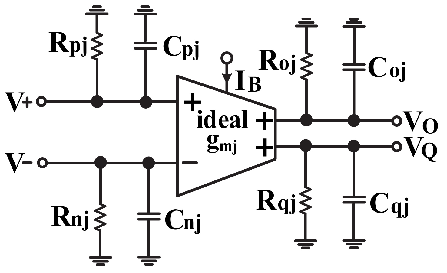
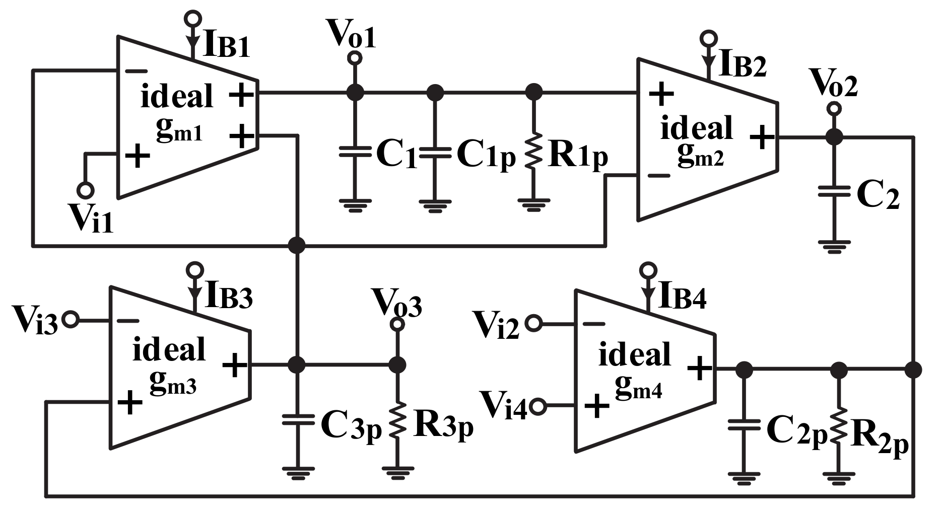
4. Effect of Non-Idealities Analysis

In this section, the non-ideal circuit model of OTA will be considered. The non-ideal terminal effects of OTA are considered, including non-ideal current transfer error parameters and non-ideal finite input and output parasitic elements. Figure 4 illustrates a non-ideal OTA model with various parasitic elements [19], where RPj, Rnj, Roj, Rqj, CPj, Cnj, Coj, and Cqj represent the finite parasitic resistances and capacitances of the input and output terminals of the jth OTA, respectively. In Figure 4, the non-ideal dual-output currents of OTA are given as IO = γgm(V+ − V−) and IQ = ηgm(V+ − V−), where γ = 1 − εγi and η = 1 − εηi. Here, εγi (|εγi|«1) and εηi (|εηi|«1) indicate the non-ideal dual-output currents of OTA current tracking errors. Taking the non-ideal OTA model into account, the biquad shown in Figure 2 can be modified to become the biquad presented in Figure 5. The effect of the non-ideal current transfer error parameters and the parasitic impedance elements on the characteristic parameters of ωo and Q has been investigated to indicate the performance of the proposed biquad. Accounting for the parasitic elements in Figure 5, the non-ideal characteristic equation, D1(s), of the equivalent circuit model in Figure 5 becomes:
D 1 ( s ) = β 1 s 2 C 1 C 2 g m 1 ( 1 + P β 1 C 1 C 2 g m 1 ) + α 2 α 3 sC 1 g m 2 g m 3 ( 1 + Q α 2 α 3 C 1 g m 2 g m 3 )   + α 1 α 2 α 3 g m 1 g m 2 g m 3 ( 1 + R α 1 α 2 α 3 g m 1 g m 2 g m 3 )
where P = C 1 C 2 G 3 p + C 1 C 3 p G 2 p + C 2 C 3 p G 1 p , Q = C 1 G 2 p G 3 p + β 1 C 1 G 2 p g m 1 + C 2 G 1 p G 3 p + β 1 C 2 G 1 p g m 1 + C 3 p G 1 p G 2 p + s 2 C 1 C 2 C 3 p , R = G 1 p G 2 p G 3 p + β 1 G 1 p G 2 p g m 1 + α 2 α 3 g m 2 g m 3 G 1 p , C 1 = C 1 + C 1 p , C 2 = C 2 + C 2 p , C 1 p = C o 1 + C p 2 , C 2 p = C o 2 + C o 4 + C p 3 , C 3 p = C q 1 + C o 3 + C n 1 + C n 2 , G 1 p = 1 R 1 p , G 2 p = 1 R 2 p , G 3 p = 1 R 3 p , R 1 p = R o 1 / / R p 2 , R 2 p = R o 2 / / R o 4 / / R p 3 , and R 3 p = R q 1 / / R o 3 / / R n 1 / / R n 2 .
According to Equation (16), non-ideal parasitic elements and non-ideal current transfer error parameters influence ωo and Q. Neglecting the third-order effects, the biquad can operate as an ideal case by satisfying the following conditions:
1 sC 1 < < R 1 p
1 sC 2 < < R 2 p
sC 3 p + G 3 p < < g m 1
Hence, D1(s) of Figure 5 can be approximated as:
D 2 ( s ) = β 1 s 2 C 1 C 2 g m 1 + α 2 α 3 sC 1 g m 2 g m 3 + α 1 α 2 α 3 g m 1 g m 2 g m 3
In this case, ωo and Q were modified as:
ω o = α 1 α 2 α 3 g m 2 g m 3 β 1 C 1 C 2
Q = g m 1 α 1 C 2 β 1 α 2 α 3 C 1 g m 2 g m 3
The sensitivities of the parameters ωo and Q in Equations (21) and (22) were not larger than unity in magnitude. Therefore, the proposed biquad can be classified as an insensitive circuit.

5. Simulation and Experimental Results

To demonstrate the feasibility of the proposed OTA-C configurations, the proposed biquad and QO were simulated in PSpice using the macro-model of LT1228 IC and were measured in the laboratory using commercially available IC from Linear Technology Inc., LT1228. The power supply was ±15 V. The transconductance gain is given by gm = 10 IB [24]. This feature makes it possible to electronically control the transconductance gain.

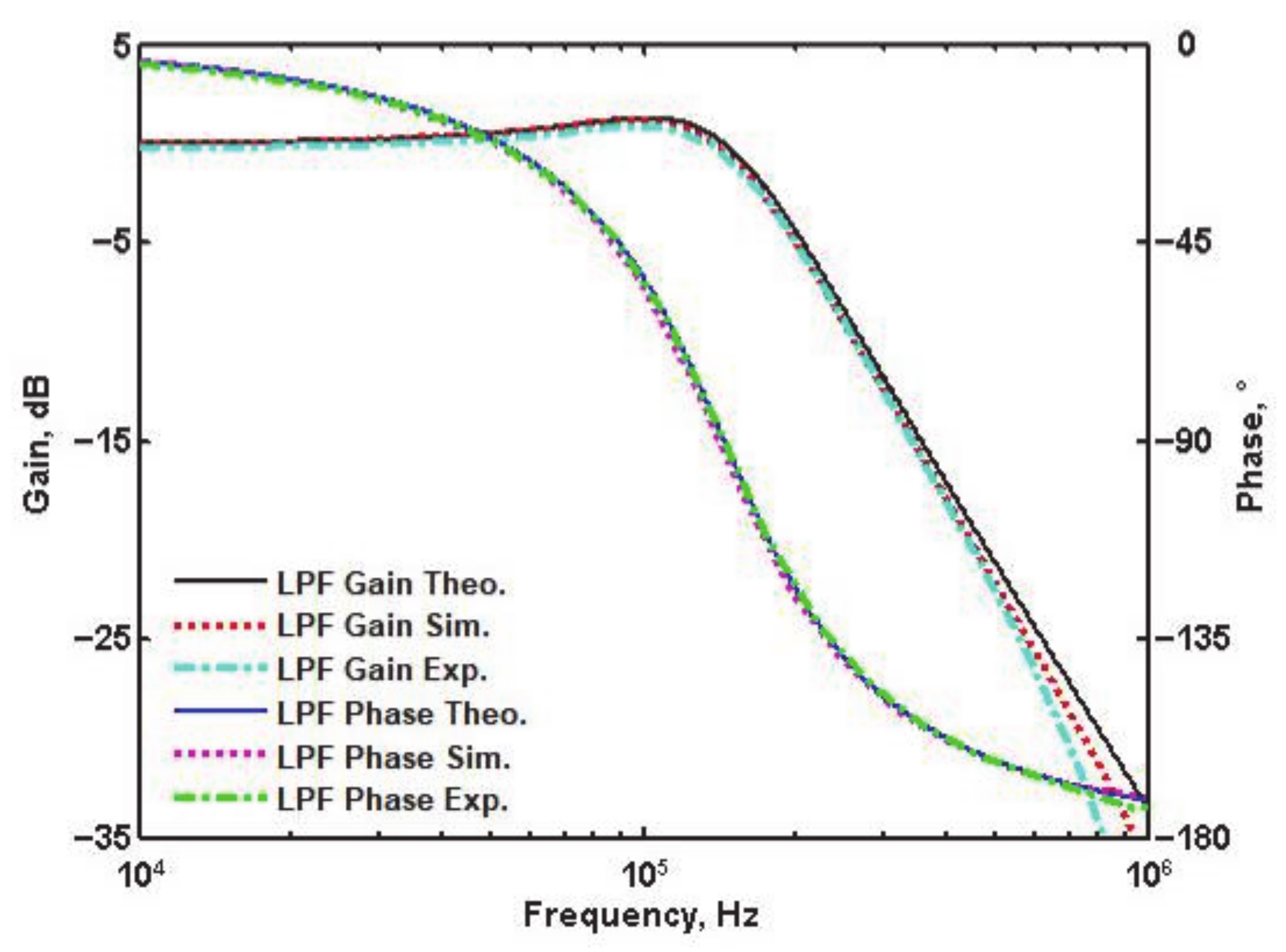
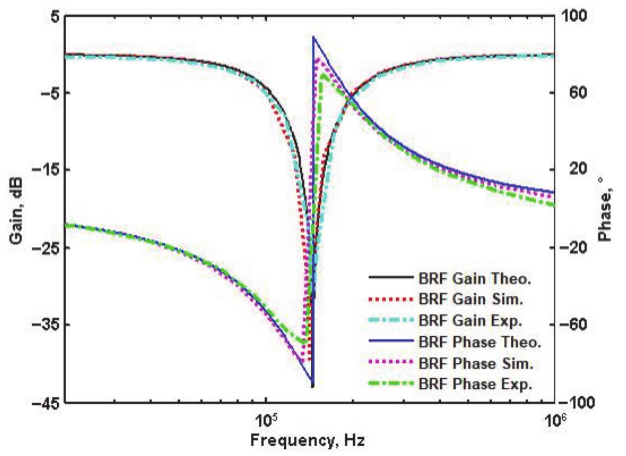
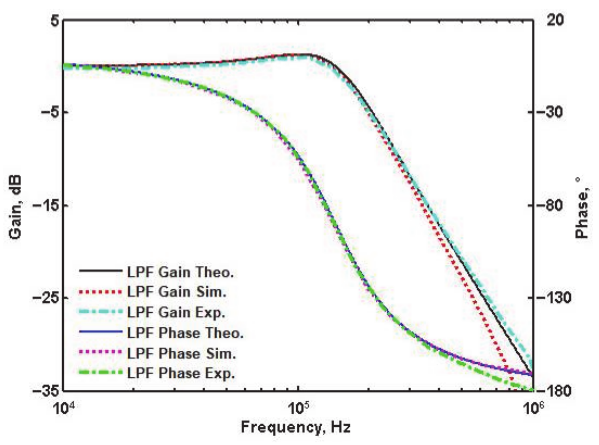
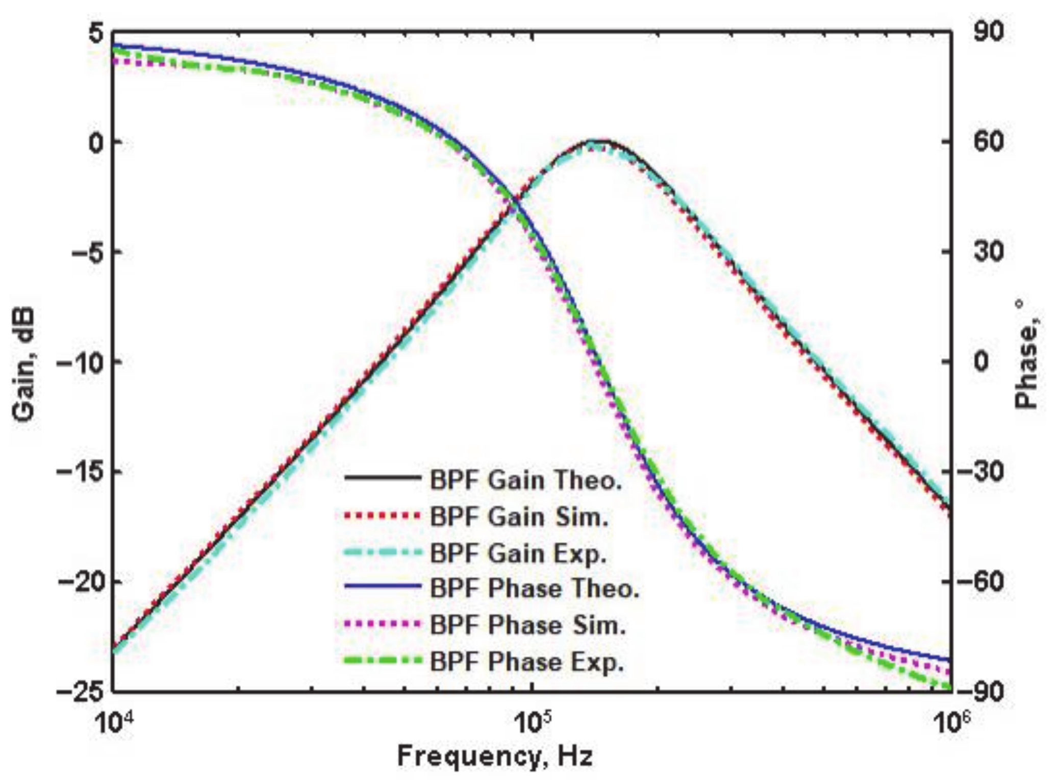
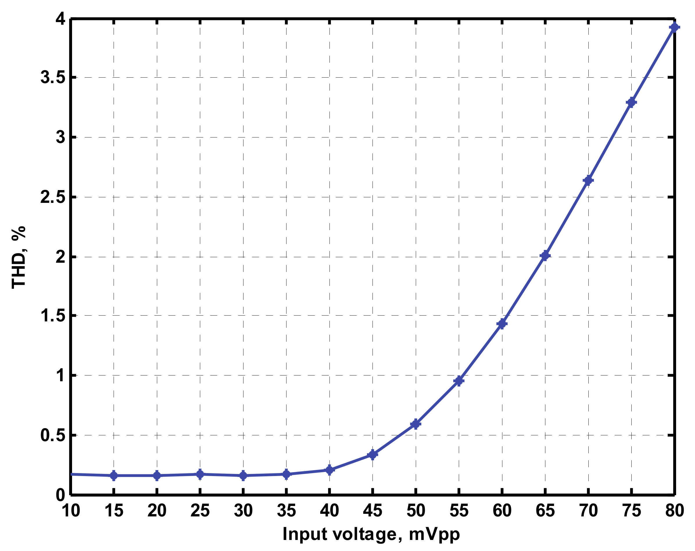
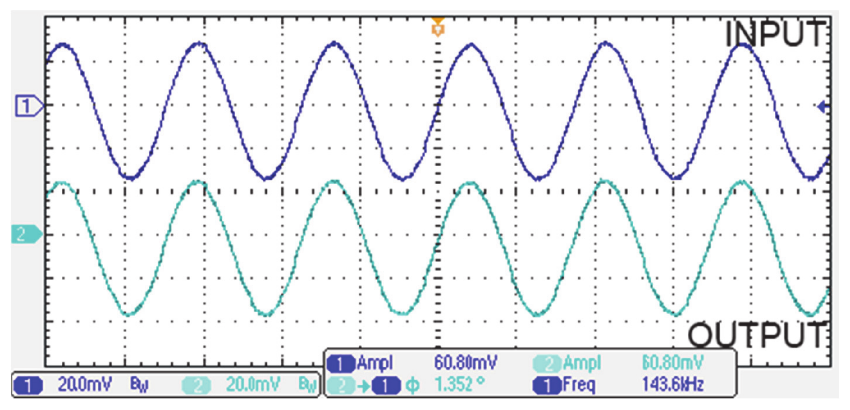
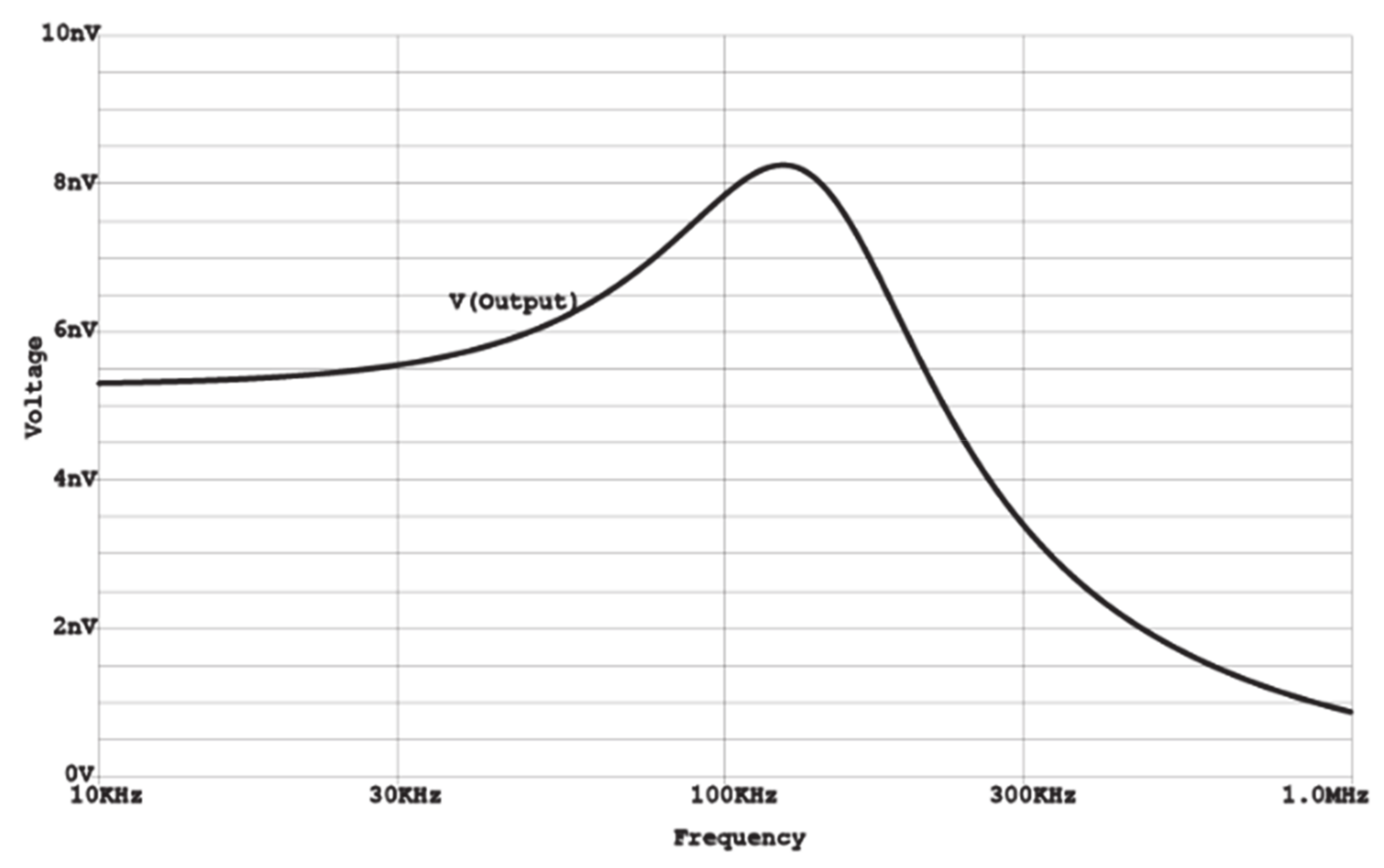
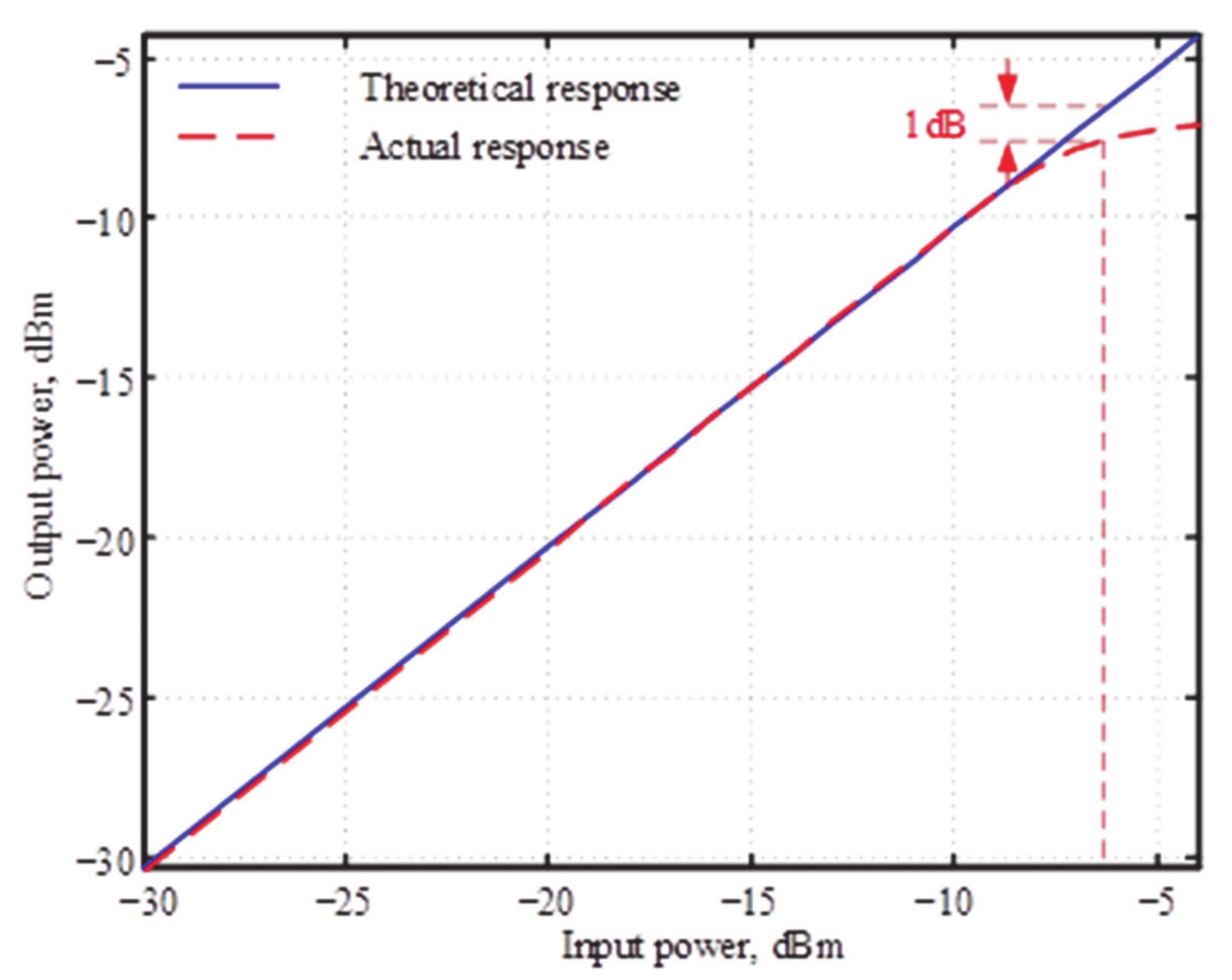
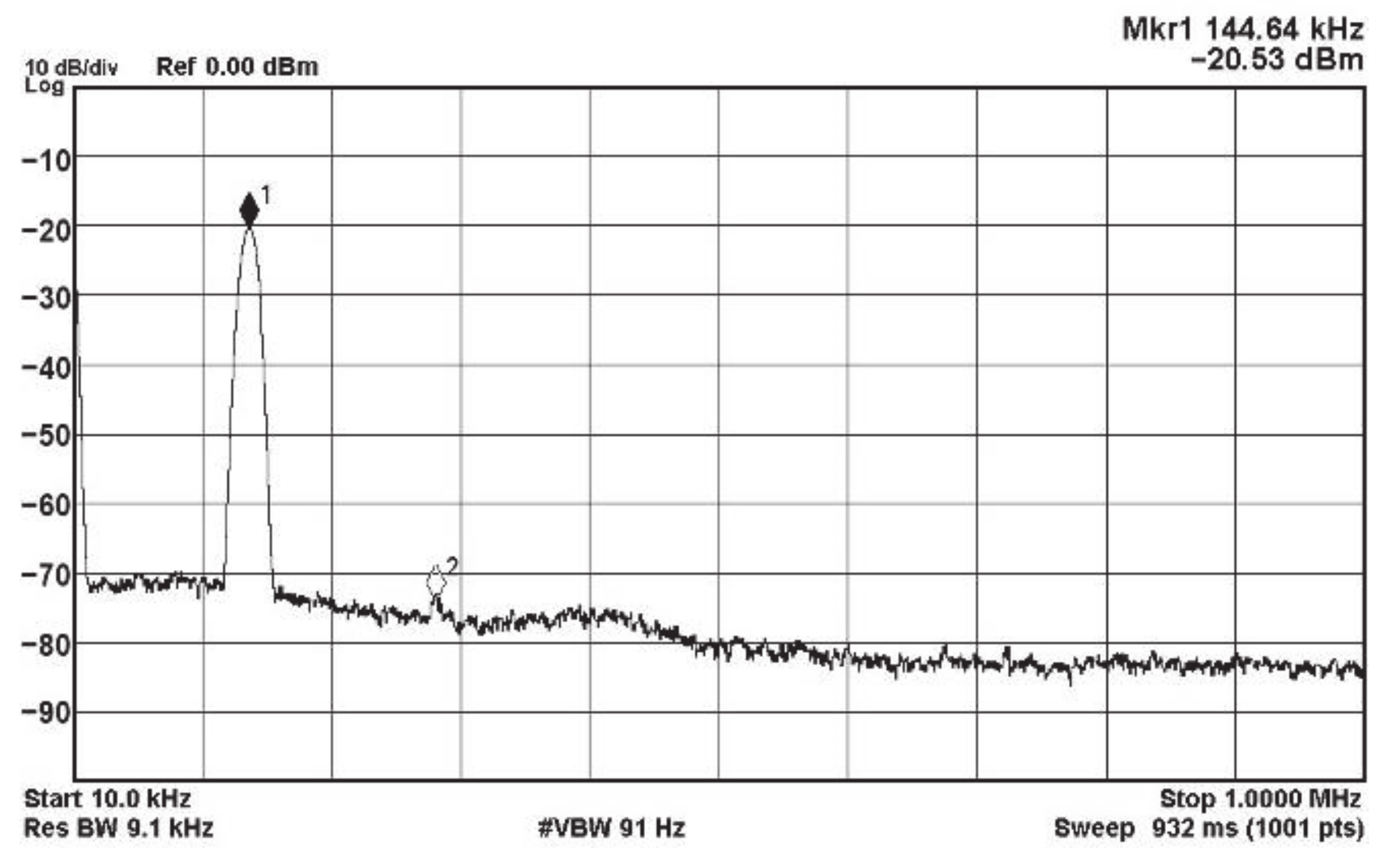
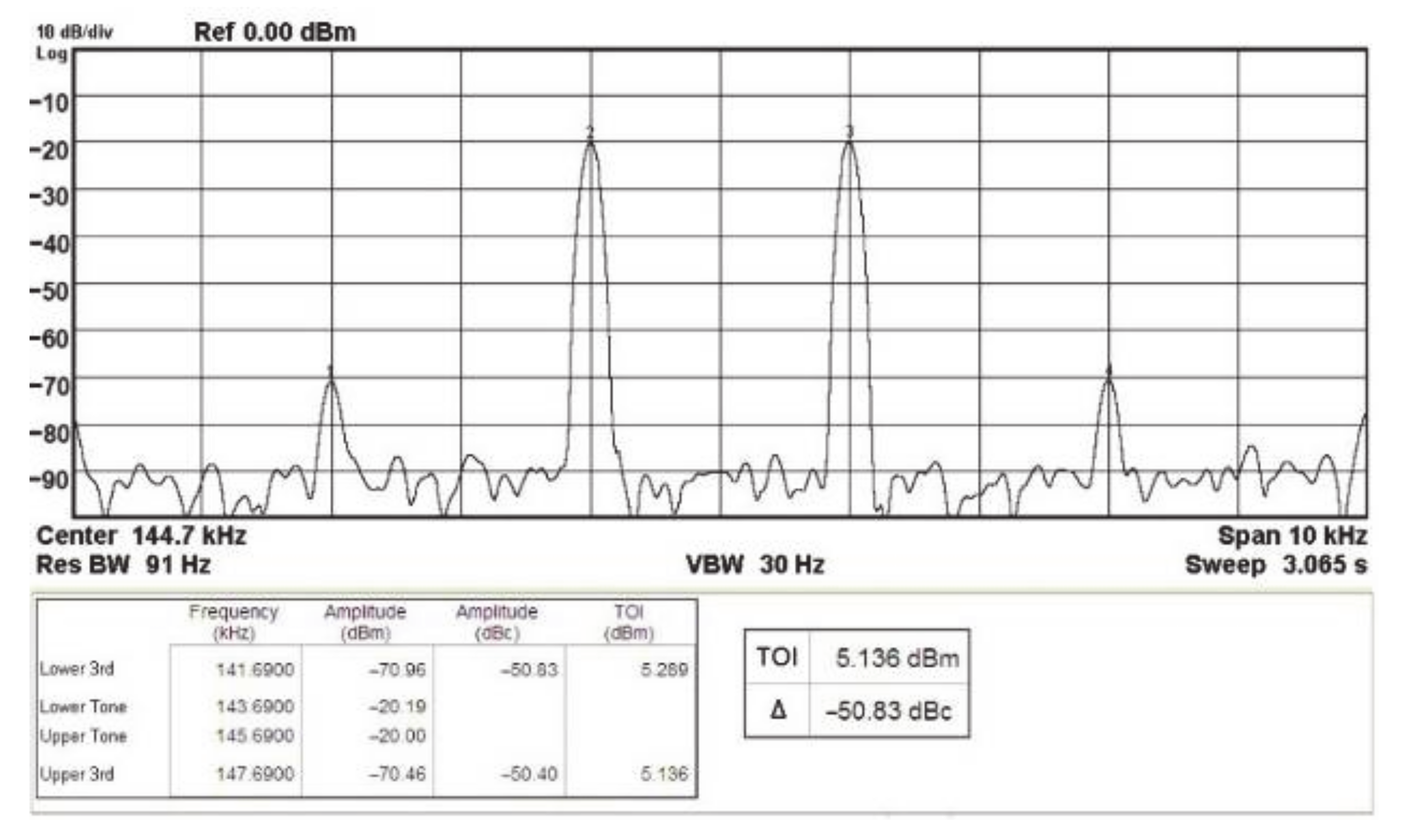
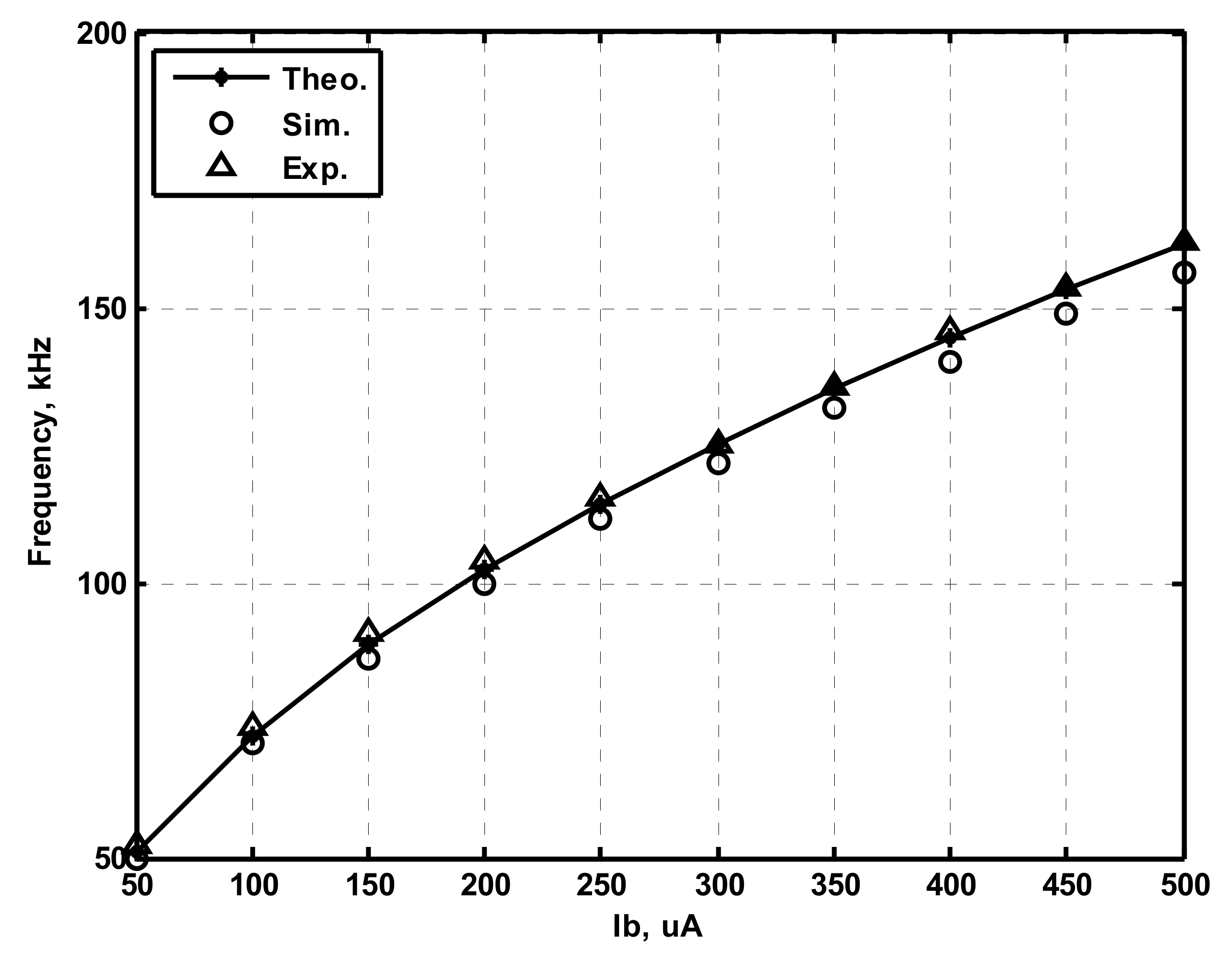
5.1. The Electronically Tunable VM Biquad

As shown in Figure 2, the capacitors C1 and C2 were chosen as 2.2 nF and the bias currents were set to IB1 = IB2 = IB3 = IB4 = 200 µA (that is, gm = 2 mS). This setting has been designed for LPF, BPF, IBPF, IHPF, BRF, and APF responses, with fo = 144.7 kHz and Q = 1. Hence, the simulation and measurement functions of the LPF (Vo1), IBPF (Vo2), and BRF (Vo3) in Part I are depicted in Figure 6, Figure 7 and Figure 8, respectively. Figure 9, Figure 10, Figure 11, Figure 12 and Figure 13 represent the simulated and measured functions of the LPF, BPF, IBPF, IHPF, and APF in Part II, respectively. The power consumption for simulation and measurement is 0.92 and 0.96 W under ±15 V of supply voltage, respectively.
To illustrate the tunable property of natural frequency, fo, without affecting the Q, the bias currents IB1 = IB2 = IB3 were given as 100, 200, and 300 µA respectively, while keeping C1 = C2 = 2.2 nF and IB4 = 200 µA. The simulation and measurement responses of the BPF on the Vo1 output terminal corresponding to different DC bias currents are shown in Figure 14, where Vi3 = Vin and Vi1 = Vi2 = Vi4 = 0. As depicted in Equation (9), Q can be used to adjust the transconductance gain, gm1, without affecting the fo. The feature of varying the Q without affecting the fo is shown in Figure 15. Q varies (Q = 1, 1.5, and 2) when fo is maintained at 144.7 kHz. In Figure 15, the IB1 was given as 200, 300, and 400 µA respectively, while keeping C1 = C2 = 2.2 nF and IB2 = IB3 = IB4 = 200 µA.
To verify the dynamic range, the proposed biquad was tested by repeating simulation of the sinusoidal input signal at fo = 144.7 kHz. Figure 16 shows the input dynamic range of the BPF on the Vo3 output terminal when only Vi4 is applied to the input signal, which indicates an amplitude of 60 mVpp (peak-to-peak) without signification distortion. The total harmonic distortion (THD) result for the BPF response is shown in Figure 17. From Figure 17, it can be obtained that the THD is about 3.92% when the input signal increases to 80 mVpp. Figure 18 shows the measurement of the BPF response, which can be extended to an amplitude of 60 mVpp without signification distortion. Figure 19 shows the simulation output noise of the BPF versus frequency. As shown in Figure 19, the maximum output noise reaches 7.937 nV/ Hz . Hence, the output noise was small and did not affect the proposed filter.
To show the linearity of the biquad proposed in Figure 2, a 1 dB power gain compression point (P1dB) of the IBPF response has been measured. Figure 20 shows the measured output P1dB of the IBPF response on the Vo2 output terminal when only Vi1 is applied to the input signal, which indicates that the measured output P1dB point is about −7 dBm. The spectrum of the IBPF response is illustrated in Figure 21. The measured angular frequency is about 144.64 kHz, which is very close to the theoretical value of 144.69 kHz. To represent the nonlinearity of the biquad proposed in Figure 2, a two-tone testing of intermodulation distortion (IMD) has been used to characterize the nonlinearity of the IBPF response on the Vo2 output terminal. Figure 22 shows the spectrum of IBPF responses obtained by applying two-tone signals, f1 and f2, near the center frequency of fo = 144.69 kHz for intermodulation characterization. In Figure 22, a low-frequency tone with f1 = 143.69 kHz and a high-frequency tone with f2 = 145.69 kHz are used, and the input amplitude is equal to 126 mVpp. The measured value of the third-order IMD (IMD3) is about −50.83 dBc, and the measured value of the third-order intercept (TOI) point is about 5.136 dBm. The figure-of-merit (FoM) of the biquad was defined as [14]:
FoM   =   Dynamic   range × f o Power   dissipation × Supply   voltage
where fo is the central frequency. According the measured IBPF frequency spectrum in Figure 21, the dynamic range between the fundamental tone and the largest spur of the spurious-free dynamic range is approximately 53.49 dB. Hence, the FoM of the proposed IBPF is approximately calculated as 268.75 × 10³.

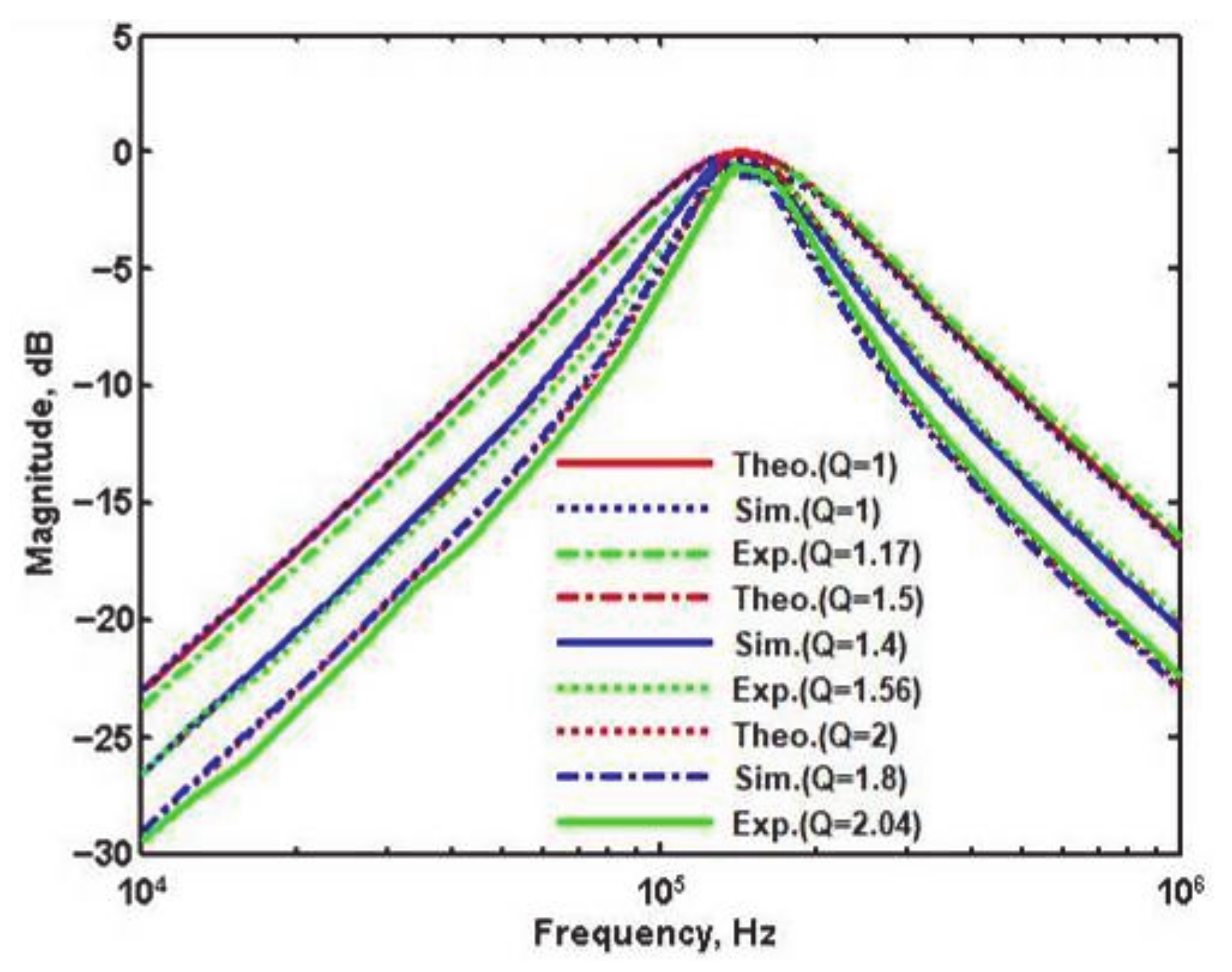
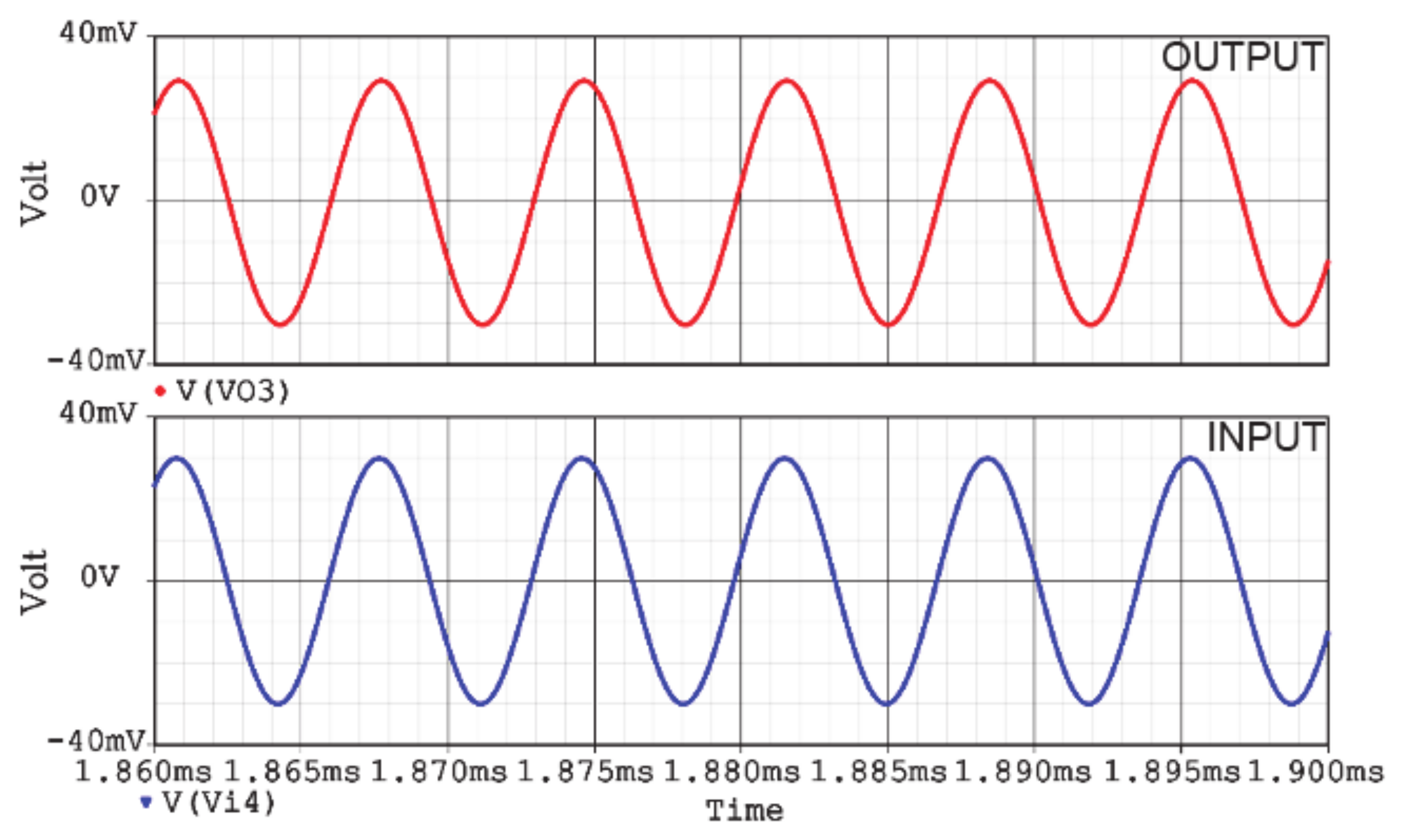
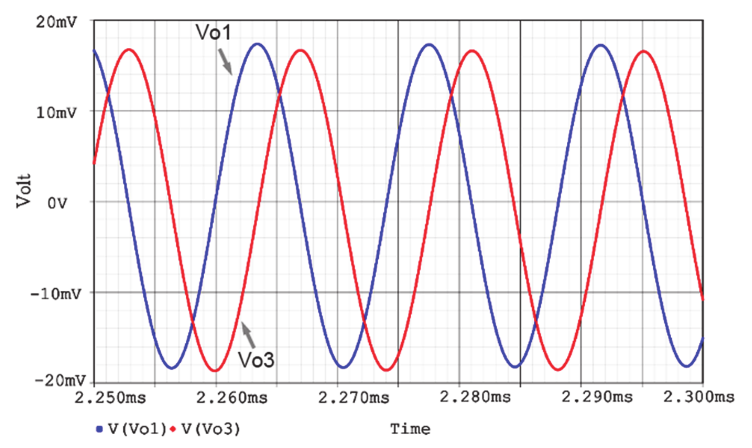
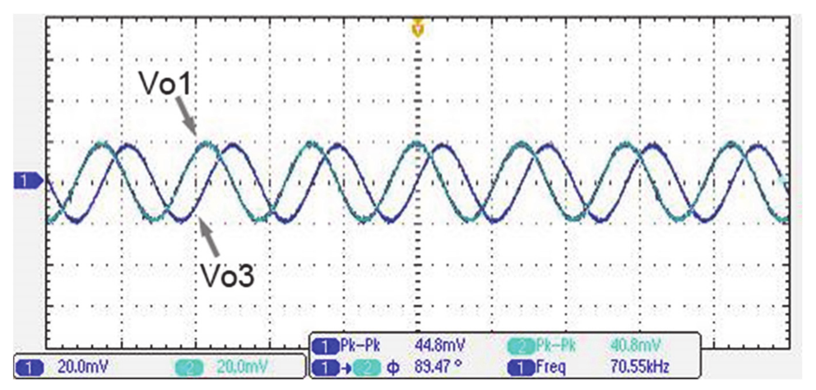
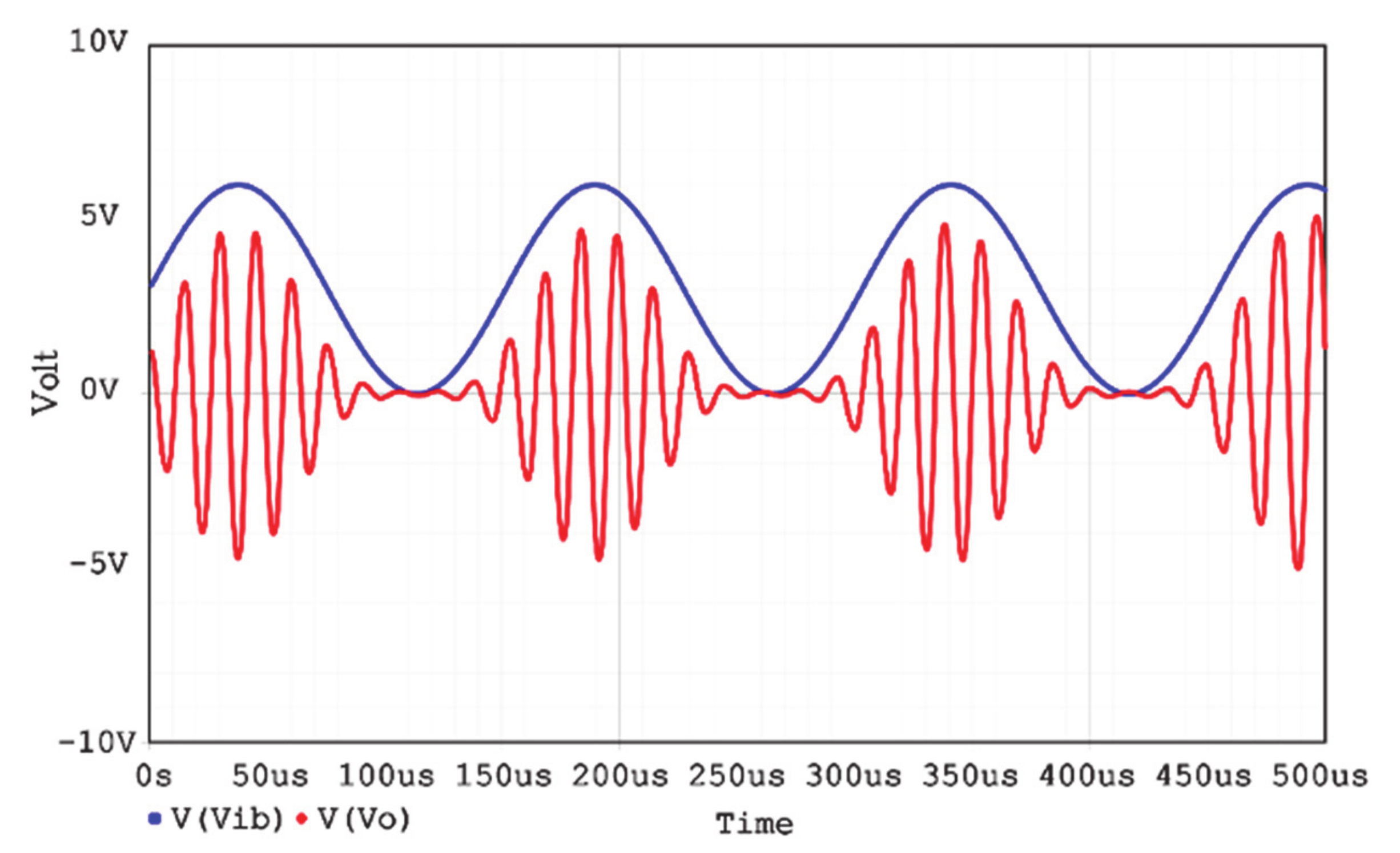
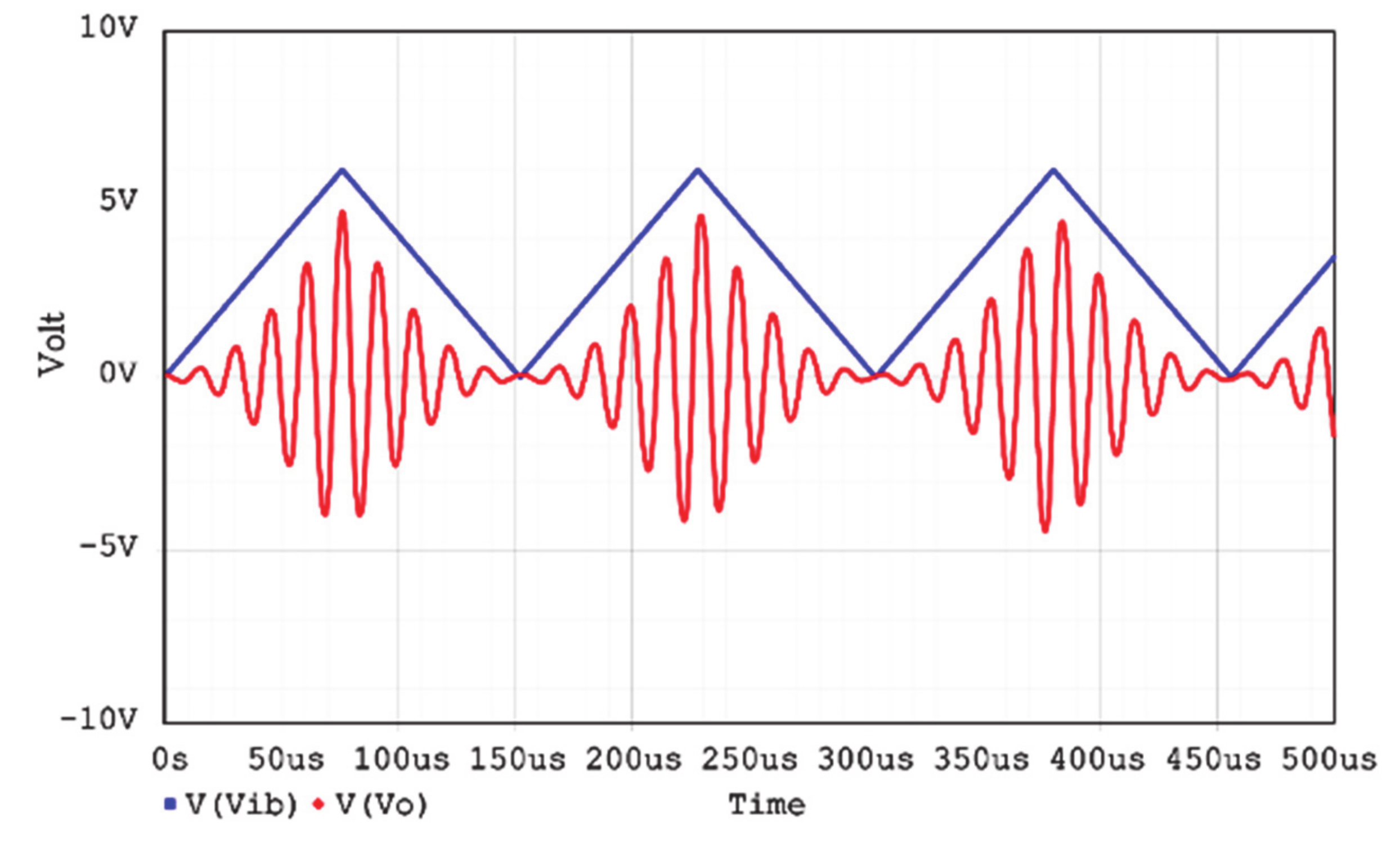
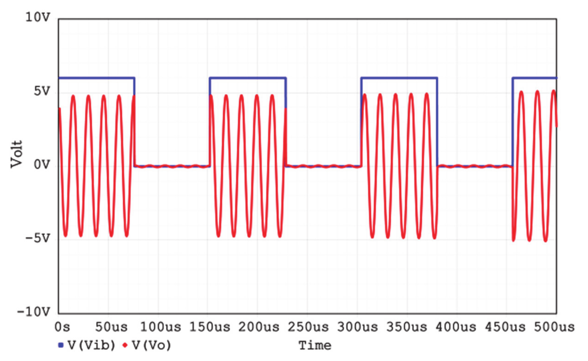
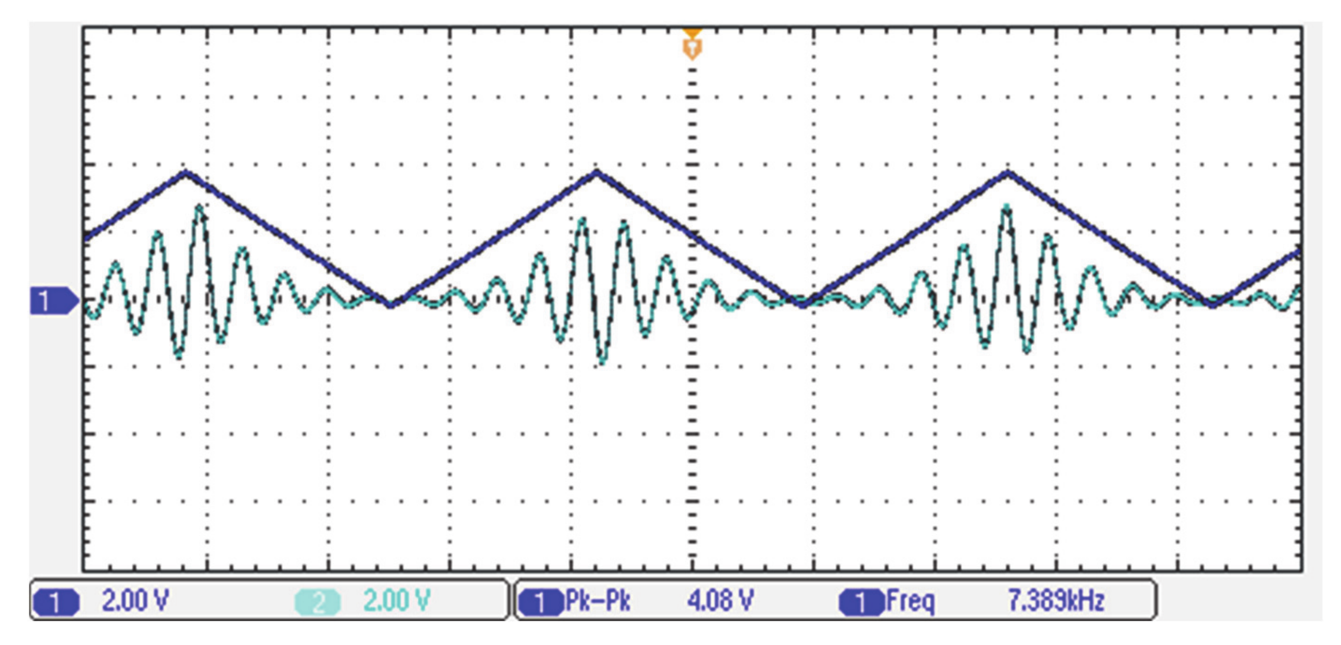
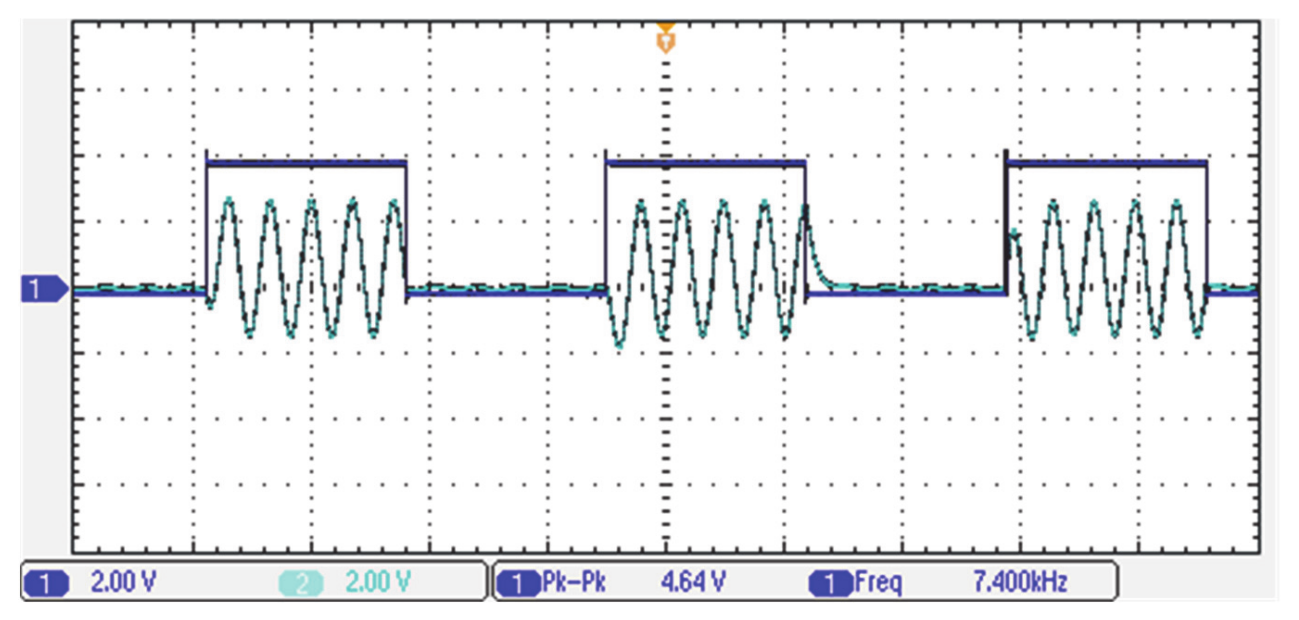
5.2. The QO with Amplitude of Output Current

To demonstrate the theoretical study, the behavior of the proposed electronically controllable OTA-C QO with amplitude of output current has been verified by simulations and experimental measurements. The QO, as shown in Figure 3, was designed for the fo = 72.3 kHz, with gm1 = 1.18 mS, gm2 = gm3 = gm4 = 1 mS, and C1 = C2 = 2.2 nF. As mentioned earlier, gm1 was designed to be greater than the theoretical value to guarantee start-up of oscillation. Figure 23 shows the simulation quadrature output voltage waveforms. It can be seen from the simulation results that the FO is approximately equal to 71 kHz, close to the theoretical value, and the error rate is −1.8%. Figure 24 represents the experimental quadrature outputs Vo1 and Vo3. According to the experimental results, the measured FO is equal to 73.78 kHz, which is close to the theoretical value, and the error rate is 2%. Figure 25 shows the simulated and experimental results of the FO by varying the values of gm3. Figure 26 shows how to calculate the phase noise using the Agilent phase noise measurement solution. The phase noise in the proposed electronically controllable OTA-C QO is lower than −74.93 dBc/Hz (at 1 kHz offset). To show the usability of the electronically controllable OTA-C QO in Figure 3, the applications of AM and ASK generators are confirmed in Figure 27, Figure 28, Figure 29, Figure 30, Figure 31 and Figure 32, where IB4 is sine wave, triangle wave, and pulse signals respectively, with a frequency of 7.4 kHz. These simulation and experimental measurements are close to the theoretical prediction, confirming the feasibility of the proposed electronically controllable OTA-C QO.

6. Conclusions

This paper presented an electronically tunable biquad and an output current amplitude, electronically tunable QO. The proposed circuits employed three OTAs, one DO-OTA, and two grounded capacitors. The single-input three-output VM multifunction biquad or the four-input single-output VM universal biquad can work in the same configuration. The proposed biquad can simultaneously realize LPF, IBPF, and BRF responses. By choosing the appropriate input terminals, the proposed biquad can realize all standard filtering functions without inverting-type voltage input signals. The characteristic parameters ωo and Q are orthogonally controllable. The measured value of the power dissipation was 0.96 W, under 32 mA constant output current. The measured P1dB value of the output IBPF was −7 dBm, and the measured IMD3 and TOI values were −50.83 dBc and 5.136 dBm, respectively. The measured value of the spurious-free dynamic range was 53.49 dB, and the FoM of the filter was 268.75 × 10³. The proposed biquad configuration can be used as a type of electronically tunable QO with high-output impedance and amplitude-controllable sinusoidal current output signal. The proposed electronically tunable QO generated two sinusoidal output voltages with 90° phase difference, and CO and FO can be adjusted independently by adjusting the IB of the OTA. Moreover, the proposed QO with electronically controllable amplitude of the sinusoidal current output signal can provide an AM signal or ASK signal, and is widely utilized in modulation systems. The proposed circuits have been verified by experiments and verified by OrCAD PSpice simulations to confirm the theoretical and expected assumptions.

Author Contributions

S.-F.W. and H.-P.C. conceived and designed the theoretical verifications; Y.K. revised the manuscript to improve the quality of English; H.-P.C. analyzed the results and wrote the paper; F.-Y.L. performed the simulations and experiments. All authors have read and agreed to the published version of the manuscript.

Funding

This research received no external funding.

Institutional Review Board Statement

Not applicable.

Informed Consent Statement

Not applicable.

Data Availability Statement

Not applicable.

Conflicts of Interest

The authors declare no conflict of interest.

References

  1. Arora, T.S.; Gupta, S. A new voltage mode quadrature oscillator using grounded capacitors: An application of CDBA. Eng. Sci. Technol. 2018, 21, 43–49. [Google Scholar] [CrossRef]
  2. Bhaskar, D.R.; Gupta, S.S.; Senani, R. New CFOA-based sinusoidal oscillators retaining independent control of oscillation frequency even under the influence of parasitic impedances. Analog Integr. Circuits Signal Process. 2012, 73, 427–437. [Google Scholar] [CrossRef]
  3. Bhaskar, D.R.; Senani, R. New CFOA-based single-element-controlled sinusoidal oscillators. IEEE Trans. Instrum. Meas. 2006, 55, 2014–2021. [Google Scholar] [CrossRef]
  4. Senani, R.; Singh, V.K. Novel single-resistance-controlled-oscillator configuration using current-feedback-amplifiers. IEEE Trans. Circuits Syst. I Fundam. Theory Appl. 1996, 43, 698–700. [Google Scholar] [CrossRef]
  5. Abuelma’atti, M.T.; Farooqi, A.A.; Alshahrani, S.M. Novel RC oscillators using the current-feedback operational amplifier. IEEE Trans. Circuits Syst. I Fundam. Theory Appl. 1996, 43, 155–157. [Google Scholar] [CrossRef]
  6. Jaikla, W.; Adhan, S.; Suwanjan, P.; Kumngern, M. Current/voltage controlled quadrature sinusoidal oscillators for phase sensitive detection using commercially available IC. Sensors 2020, 20, 1319. [Google Scholar] [CrossRef] [PubMed] [Green Version]
  7. Kumari, S.; Gupta, S.; Pandey, N.; Pandey, R.; Anurag, R. LC-ladder filter systematic implementation by OTRA. Eng. Sci. Technol. 2016, 19, 1808–1814. [Google Scholar] [CrossRef] [Green Version]
  8. Verma, R.; Pandey, N.; Pandey, R. CFOA based low pass and high pass fractional step filter realizations. AEU Int. J. Electron. Commun. 2019, 99, 161–176. [Google Scholar] [CrossRef]
  9. Liao, P.H.; Hwang, Y.S.; Chen, J.J.; Ku, Y.; Wang, S.F. A new low-voltage operational transconductance amplifier with push-pull CMFB scheme for low-pass filter applications. AEU Int. J. Electron. Commun. 2020, 123, 153298. [Google Scholar] [CrossRef]
  10. Tangsrirat, W.; Channumsin, O. High-input impedance voltage-mode multifunction filter using a single DDCCTA and grounded passive elements. Radioengineering 2011, 20, 905–910. [Google Scholar]
  11. Yuce, E.; Verma, R.; Pandey, N.; Minaei, S. New CFOA-based first-order all-pass filters and their applications. AEU Int. J. Electron. Commun. 2019, 103, 57–63. [Google Scholar] [CrossRef]
  12. Minaei, S.; Yuce, E. All-grounded passive elements voltage-mode DVCC-based universal filters. Circuits Syst. Signal. Process. 2010, 29, 295–309. [Google Scholar] [CrossRef]
  13. Yuce, E.; Tez, S. A novel voltage-mode universal filter composed of two terminal active devices. AEU Int. J. Electron. Commun. 2018, 86, 202–209. [Google Scholar] [CrossRef]
  14. Alpaslan, H.; Yuce, E. DVCC+ based multifunction and universal filters with the high input impedance features. Analog Integr. Circuits Signal. Process. 2020, 103, 325–335. [Google Scholar] [CrossRef]
  15. Acosta, L.; Jimenez, M.; Carvajal, R.G.; Lopez-Martin, A.J.; Ramirez-Angulo, J. Highly linear tunable CMOS gm-C low-pass filter. IEEE Trans. Circuits Syst. I Regul. Pap. 2009, 56, 2145–2158. [Google Scholar] [CrossRef]
  16. Tao, Y.; Fidler, J.K. Electronically tunable dual-OTA second-order sinusoidal oscillators/filters with non-interacting controls: A systematic synthesis approach. IEEE Trans. Circuits Syst. I Fundam. Theory Appl. 2000, 47, 117–129. [Google Scholar]
  17. Tu, S.H.; Hwang, Y.S.; Chen, J.J.; Soliman, A.M.; Chang, C.M. OTA-C arbitrary-phase-shift oscillators. IEEE Trans. Instrum. Meas. 2012, 61, 2305–2319. [Google Scholar] [CrossRef]
  18. Kumar, K.; Pal, K. Voltage mode multifunction OTA-C biquad filter. Microelectron. Int. 2006, 23, 24–27. [Google Scholar] [CrossRef]
  19. Kumar, K.; Pal, K.; Gupta, G.K. Realization of multi-function biquad filter using operational transconductance amplifier. Indian J. Pure Appl. Phy. 2006, 44, 71–74. [Google Scholar]
  20. Kumngern, M.; Suwanjan, P.; Dejhan, K. Electronically tunable voltage-mode universal filter with single-input five-output using simple OTAs. Int. J. Electron. 2013, 100, 1118–1133. [Google Scholar] [CrossRef]
  21. Bhaskar, D.R.; Raj, A.; Kumar, P. Mixed-mode universal biquad filter using OTAs. J. Circuits, Syst. Comput. 2020, 29, 2050162. [Google Scholar] [CrossRef]
  22. Senani, R. New OTA-C universal current-mode/trans-admittance biquads. IEICE Electron. Exp. 2005, 2, 8–13. [Google Scholar]
  23. Lee, C.N. High-order multiple-mode and trans-admittance mode OTA-C universal filters. J. Circuits Syst. Comput. 2012, 21, 1520048. [Google Scholar] [CrossRef]
  24. LT1228–100 MHz Current Feedback Amplifier with DC Gain Control. Linear Technology Corporation Version Number D. 2012. Available online: http://www.linear.com/product/LT1228 (accessed on 1 October 2019).
  25. Psychalinos, C.; Kasimis, C.; Khateb, F. Multiple-input single-output universal biquad filter using single output operational transconductance amplifiers. AEU Int. J. Electron. Commun. 2018, 93, 360–367. [Google Scholar] [CrossRef]
  26. Kumngern, M.; Suksaibul, P.; Khateb, F. Four-input one-output voltage-mode universal filter using simple OTAs. J. Circuits Sys. Comp. 2019, 28, 1950078. [Google Scholar] [CrossRef]
  27. Wang, S.F.; Chen, H.P.; Ku, Y.; Yang, C.M. A voltage-mode universal filter using five single-ended OTAs with two grounded capacitors and a quadrature oscillator using the voltage-mode universal filter. Opt. Int. J. Light Electron. Opt. 2019, 192, 162950. [Google Scholar] [CrossRef]
  28. Wang, S.F.; Chen, H.P.; Ku, Y.; Lin, Y.C. Versatile tunable voltage-mode biquadratic filter and its application in quadrature oscillator. Sensors 2019, 19, 2349. [Google Scholar] [CrossRef] [PubMed] [Green Version]
  29. Wang, S.F.; Chen, H.P.; Ku, Y.; Yang, C.M. Independently tunable voltage-mode OTA-C biquadratic filter with five inputs and three outputs and its fully-uncoupled quadrature sinusoidal oscillator application. AEU Int. J. Electron. Commun. 2019, 100, 152822. [Google Scholar] [CrossRef]
  30. Wang, S.F.; Chen, H.P.; Ku, Y.; Lee, C.L. Versatile voltage-mode biquadratic filter and quadrature oscillator using four OTAs and two grounded capacitors. Electronics 2020, 9, 1493. [Google Scholar] [CrossRef]
Figure 1. Symbol of the OTA. (a) Single-ended output OTA and (b) DO-OTA.
Applsci 11 07357 g001
Figure 2. Proposed VM OTA-C biquad.
Applsci 11 07357 g002
Figure 3. Proposed VM OTA-C QO with amplitude of output current.
Applsci 11 07357 g003
Figure 4. The non-ideal OTA with its parasitic resistors and capacitors.
Applsci 11 07357 g004
Figure 5. The influence of parasitic components on the proposed VM biquad.
Applsci 11 07357 g005
Figure 6. Comparison of LPF experimental response, simulated response, and theoretical response in Part I.
Applsci 11 07357 g006
Figure 7. Comparison of IBPF experimental response, simulated response, and theoretical response in Part I.
Applsci 11 07357 g007
Figure 8. Comparison of BRF experimental response, simulated response, and theoretical response in Part I.
Applsci 11 07357 g008
Figure 9. Comparison of LPF experimental response, simulated response, and theoretical response in Part II.
Applsci 11 07357 g009
Figure 10. Comparison of BPF experimental response, simulated response, and theoretical response in Part II.
Applsci 11 07357 g010
Figure 11. Comparison of IBPF experimental response, simulated response, and theoretical response in Part II.
Applsci 11 07357 g011
Figure 12. Comparison of IHPF experimental response, simulated response, and theoretical response in Part II.
Applsci 11 07357 g012
Figure 13. Comparison of APF experimental response, simulated response, and theoretical response in Part II.
Applsci 11 07357 g013
Figure 14. Gain characteristics of the BPF with different fo.
Applsci 11 07357 g014
Figure 15. Gain characteristics of the BPF with different Q.
Applsci 11 07357 g015
Figure 16. Time-domain BPF input and output voltage signals.
Applsci 11 07357 g016
Figure 17. THD variations of the BPF against applied input voltages.
Applsci 11 07357 g017
Figure 18. Time-domain BPF input and output experimental voltage signals.
Applsci 11 07357 g018
Figure 19. Noise simulation results of BPF against frequency.
Applsci 11 07357 g019
Figure 20. The measurement of P1dB at the Vo2 output terminal.
Applsci 11 07357 g020
Figure 21. Frequency spectrum of the IBPF at the Vo2 output terminal.
Applsci 11 07357 g021
Figure 22. The IBPF output spectrum of Vo2 for a two-tone -IMD test.
Applsci 11 07357 g022
Figure 23. The steady-state simulation waveform of the quadrature voltage outputs.
Applsci 11 07357 g023
Figure 24. Measured result of quadrature voltage waveforms.
Applsci 11 07357 g024
Figure 25. Results of the FO by varying gm3.
Applsci 11 07357 g025
Figure 26. Measured result of the phase noise.
Applsci 11 07357 g026
Figure 27. The simulation result of the AM signal generator using sine wave input signal.
Applsci 11 07357 g027
Figure 28. The simulation result of the AM signal generator using triangle wave input signal.
Applsci 11 07357 g028
Figure 29. The simulation result of the ASK signal generator using pulse wave input signal.
Applsci 11 07357 g029
Figure 30. The measurement result of the AM signal generator using sine wave input signal.
Applsci 11 07357 g030
Figure 31. The measurement result of the AM signal generator using triangle wave input signal.
Applsci 11 07357 g031
Figure 32. The measurement result of the ASK signal generator using pulse wave input signal.
Applsci 11 07357 g032
Table 1. Comparison of the proposed biquad and the biquads previously reported in the literature [25,26,27,28,29,30].
Features[25][26][27][28][29][30]Proposed
Active and passive elements6 OTAs, and 2 C 6 OTAs, 2 Rmos, and 2 C5 OTAs, and 2 C5 OTAs, and 2 C5 OTAs, and 2 C1 DO-OTA, 3 OTAs, and 2 C1 DO-OTA, 3 OTAs, and 2 C
Resistorless structureyesnoyesyesyesyesyes
Component-matching condition (R = 1/gm)noyesnonononono
Using grounded passive elementsyesyesyesyesyesyesyes
No inverting-type input signalyesyesyesyesyesyesyes
High-input impedancesyesyesyesyesyesyesyes
Orthogonal control of ωo and Qyesyesyesyesyesyesyes
Versatile input/output functionsnononoyesyesyesyes
Simultaneously realizing three filtering functionsnononoyesyesyesyes
Offering five standard filtersyesyesyesyesyesyesyes
Easily transformed into a QO with output current amplitudenonononononoyes
Easily realizing oscillator with AM/ASK signalsnonononononoyes
Note: QO: quadrature oscillator; AM: amplitude modulation; ASK: amplitude shift keying.
Table 2. Characteristic comparisons of the proposed biquad with the biquads previously reported in the literature [25,26,27,28,29,30].
Features[25][26][27][28][29][30]Proposed
Power supply±15 V±5 V±15 V±15 V±15 V±15 V±15 V
Verification of simulation/measurementyes/yesyes/yesyes/yesyes/yesyes/yesyes/yesyes/yes
Simulated the power dissipation (W)nonenonenonenone0.860.920.92
Measured the power dissipation (W)nonenonenone0.861.21.230.96
Central frequency of the filter (kHz)1032.9238.7159.15217144.7144.7
Maximum output noise (nV/ Hz )nonenonenonenonenonenone7.937
Measured the output P1dB point (dBm)nonenonenone−9.2none−5.9−7
Measured the TOI point (dBm)nonenonenone−5.66none−2.5975.136
Measured the IMD3 (dBc)nonenone−30.03 (@ 80 mVpp)−42.35 (@ 60 mVpp)−31.16 (@ 90 mVpp)−48.67 (@ 63 mVpp)−50.83 (@ 126 mVpp)
FoM (×103)nonenonenonenonenonenone268.75
Note: P1dB: 1 dB power gain compression; TOI: third-order intercept; IMD3: third-order intermodulation distortion; FoM: figure-of-merit.
Publisher’s Note: MDPI stays neutral with regard to jurisdictional claims in published maps and institutional affiliations.

