Abstract
Flow of photocurrent through the metal-oxide-semiconductor structure induced by the pulsed infrared CO2 laser is investigated experimentally. In the case of a perfect insulator, the photocurrent has a photocapacitive character. Its rise is based on the hot carrier phenomenon; no carrier generation is present, only redistribution of laser-heated carriers takes place at the semiconductor surface. The magnitude of this displacement current is related to the capacitance of the structure and is dependent on the rate of the laser pulse change as well as on the laser light intensity. This effect can find application in the detection of fast infrared laser pulses as well as in the development of infrared photovaractors. Operation of such devices would not require cryogenic temperatures what is usually needed by the long-wavelength infrared semiconductor technique.
1. Introduction
Capacitors with optically-variable properties attract research interest due to their potential application in a variety of electronics devices. For example, the search for sustainable electric power supply is currently concentrated on photo-powered energy sources, and photocapacitors are an innovation in this field with promising applications in integrated devices such as medical sensors [1,2] and next generation solar cells [3,4,5,6]. Furthermore, the property of light-dependent capacitance of photovaractors is useful for optical control or modulation of microwave signals [7,8]. It should be noted that all these optical devices operate on the basis of carrier generation, i.e., when light photon energy is not less than a semiconductor forbidden energy gap.
If the photon energy is smaller than the band gap, free carrier absorption takes place in a semiconductor leading to the increase of their energy. Such free carriers having energy higher than the equilibrium one are called hot carriers. Carriers in a semiconductor can be heated not only by means of infrared radiation but also by a strong electric fields or microwaves. As a rule, no carrier generation is present during the carrier heating process. Two advantageous properties of the phenomenon can be highlighted. First, free carrier absorption is not a radiation wavelength-selective process. Second, the speed of the hot carrier effect is determined by the carrier energy relaxation time which is of picosecond order in most semiconductors. Thus, the hot carrier effect attracts interest not only from the fundamental point of view but it also finds a lot of applications. For example, it is employed in the detection of microwave [9,10] and infrared radiation [11], and even within the whole region between both these ranges including the THz frequencies [12,13]. In addition, the concept of hot carrier solar cell as remained an important focus of research topics during the last several decades [14,15,16].
When a potential barrier is present in a semiconductor, carrier heating causes their redistribution in the vicinity of it. This may result in the rise of so-called hot carrier thermo-electromotive force across the barrier. Early investigations of microwave impact on a semiconductor surface space charge region enabled the authors to conclude that carrier heating leads to the change of the surface potential [17]. The authors studied the rise of thermo-electromotive force across a metal-insulator (oxide)-semiconductor (MOS) structure, Al-SiO2-n-Si, illuminated with 10 GHz frequency microwaves. When silicon p-n diodes were exposed to microwave radiation, hot carrier thermo-emf was also induced [18], and analysis of its pulse’s kinetics brought the authors to the conclusion that the thermo-emf is determined by the discharge of capacitance of the reverse biased p-n junction.
CO2 laser light also causes a rise of the hot carrier thermo-emf across wideband semiconductor l-h [19,20] and p-n junctions [21,22,23]. It is worth noting that the hot carrier photocurrent flows in the opposite direction to the classical generation-induced photocurrent, i.e., the heated carriers diffuse the potential barrier. In the case of the reverse biased junction, when the carriers cannot overcome the potential barrier, the photocurrent pulse is still detected [22]. It was supposed that such photosignal rise was related to the p-n barrier capacitance. Later, it was assumed that carrier heating causes a change of the barrier capacitance, and this phenomenon was called a photocapacitive effect [24].
In this communication, we report photosignals induced by infrared CO2 laser radiation across an Al-SiO2-p-Si structure. The work is remarkable in two ways. First, we declare a hot carrier photocapacitive effect in a MOS device—no carrier generation is present since the laser photon energy is much lower than the silicon energy bandgap, 0.12 eV < 1.12 eV. Second, we evidence a laser induced hot carrier photocurrent under conditions when no conduction photocurrent can flow through the insulating layer of the MOS structure.
2. Experimental
Boron doped p-type silicon substrate was taken as the base of the samples; impurity concentration was (1 ÷ 1.5) × 1015 cm−3, and plane orientation was (100). The insulating 47 nm-thick SiO2 layer was grown by means of dry thermal oxidation at 1050 °C for 20 min in the SDO-125/3 quartz tube furnace (Termotron, Bryansk, USSR). The ohmic contacts were created by thermal evaporation of Al in the vacuum equipment Vaksis PVD Vapor-5S_Th” (Vaksis, Ankara, Turkey) and subsequent annealing in nitrogen atmosphere for 10 min at 450 °C. Later, aluminum was thermally deposited to form the MOS contacts. The 0.5 mm-diameter contacts were shaped by ordinary photolithography process.
The current-voltage (I-V) characteristics were measured in the dc regime using Agilent 6613C (Keysight Technologies Inc., Santa Rosa, CA, USA) power supply and Agilent 34401A multimeter, and the capacitance-voltage (C-V) dependencies were tested with Agilent E4980A LCR meter at 1 kHz frequency. A Q-switched CO2 laser was used as a source of infrared radiation: wavelength 10.6 μm, pulse duration 150 ns, repetition rate 40 Hz, and maximum intensity 1.2 MW/cm2. The laser beam was directed purely onto the MOS structure from the semiconductor side thus avoiding additional photosignal formation across the p-p+ junction of the ohmic contact [19]. The magnitude of photocurrent, i.e., photovoltage across the 50 Ω load resistor, and its temporal shape was investigated using 4 GSa/s sampling rate oscilloscope Agilent DSO6102A. The schematic of the sample and measurement scheme are presented in Figure 1. Two typical types of the samples were chosen for the investigation: those having perfectly insulating oxide (MOS-1), and those slightly conducting dc current (MOS-2).
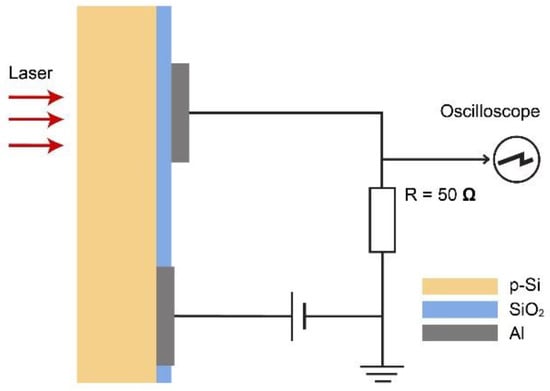
Figure 1.
Schematic of the Al-SiO2-p-Si sample and the circuit of photocurrent measurement.
3. Results and Discussion
The measured C-V characteristics of the fabricated MOS structures are presented in Figure 2. The dependencies have shapes typical of the classical metal-insulator-semiconductor structure which, as shown in the inset of Figure 2, is composed of two capacitors connected in series: CS related to a semiconductor, and another, Ci, associated with an insulator. The total capacitance of the structure Ctot is equal to
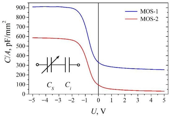
Figure 2.
Capacitance of the MOS structures versus applied voltage. In inset: diagram of a MOS structure as a series circuit of two capacitors, variable CS and fixed Ci.
In this pair, only CS is dependent on applied voltage. At reverse voltage (as a rule, reverse bias voltage agrees with its positive potential applied on the p-type semiconductor of a MOS structure [25]), holes of the p-Si are accumulated at the semiconductor surface, CS increases and exceeds the value of Ci, and the total capacitance of the structure gets close to Ci [25]. The difference in C/A magnitude of two representative samples, MOS-1 and MOS-2, can be explained by their different I-V characteristics (Figure 3). The SiO2 oxide of the MOS-1 is a perfect insulator, and no detectable dc current flows across the sample. In contrast, the MOS-2 sample demonstrates leakage current both under forward and reverse bias voltages. Since the semiconductor is of p-type conductivity, stronger current flows in the reverse bias case.
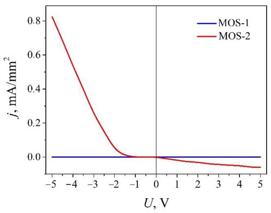
Figure 3.
Current-voltage characteristics of the MOS structures.
Photocurrent is induced when the MOS structures are exposed to the pulsed CO2 laser light. In the case of “perfect” MOS-1 sample, photovoltage of negative polarity with respect to the grounded terminal is detected when reverse bias is applied (see measurement scheme in Figure 1), and the corresponding photocurrent maximum value increases sharply with the reverse bias and then saturates (Figure 4a, blue solid dots). Much weaker photosignal of opposite polarity (blue open dots) is observed under the forward bias. Typical photocurrent pulse through the MOS-1 sample is shown in Figure 4b. Its dual-polarity shape is similar to an inherent feature of a charging-discharging capacitor. Comparison of curves of MOS-1 in Figure 2 and Figure 4a implies that the photocurrent is most probably related to the capacitance of the structure. The main noteworthy difference in the course of these two dependencies is higher reverse voltage values at which saturation of the C-V characteristic begins. Most of the bias voltage applied on the MOS structure falls on the insulator, and the only capacitance that is varied by the voltage is that of the semiconductor surface. To find how CS varies with the applied voltage, we used Equation (1) and data of the Ctot-V dependence (Figure 2). The result is depicted in Figure 5 in open orange symbols. For comparison, photocurrent versus the voltage is also shown in the picture. Good agreement between the calculated and measured results is seen.
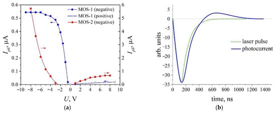
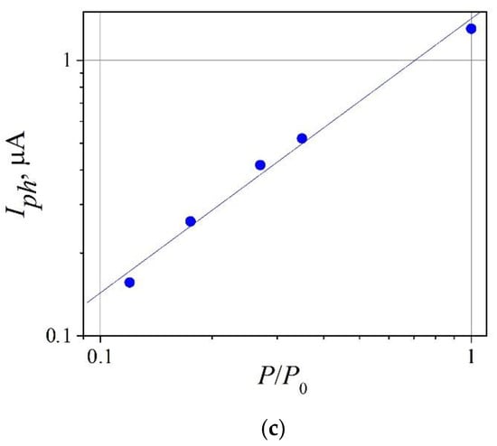
Figure 4.
(a) Photocurrent versus applied bias voltage. In the legend: “positive” and “negative” indicate photovoltage potential on the load resistor with respect to the ground (see Figure 1). (b) Laser pulse (dotted green) and photocurrent pulse (solid blue) through the MOS-1 sample. (c) Photocurrent through the MOS-1 sample versus laser intensity (P0 = 1.2 MW/cm2) at −2 V bias voltage. The straight line is guide for the eye of linear dependence.
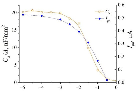
Figure 5.
Dependencies of semiconductor surface layer capacitance CS (open orange dots, left axis) and laser induced photocurrent Iph (solid blue dots, right axis) on reverse bias voltage across the MOS-1 sample.
The origin of the photocurrent through the “perfect” MOS-1 structure can be explained as follows. When reverse bias is applied, holes accumulate at the p-type semiconductor surface. When heated by the laser, they diffuse to the bulk of the semiconductor, in this way decreasing the accumulated charge (Figure 6a). Capacitance of the structure CS is altered, and the displacement current flows in the circuit. In the case of forward bias, depletion of the semiconductor surface further followed by inversion (collection of electrons) takes place. Since the semiconductor is of p-type conductivity, density of electrons collected at the surface is much lower than that was for the holes, and the heated-electron-caused photocurrent is negligible (Figure 6b). Polarity of the photocurrent supports this model—negative potential with respect to the grounded terminal is induced across the load resistor in the case of reverse bias, and the sign changes to the opposite one when the forward bias is applied. Linear dependence of the photocurrent on the laser intensity supports the hot carrier model of the photoresponse formation (Figure 4c).
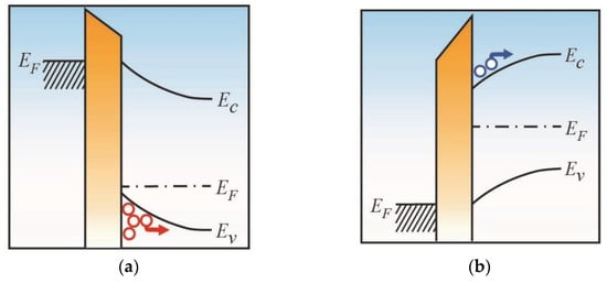
Figure 6.
Energy band diagram of the structure and model of photoresponse formation under reverse (a) and forward (b) bias voltage.
Since the photocurrent has a capacitive nature, it can be expressed as
where QS is the charge accumulated at the semiconductor surface, and ψS stands for the semiconductor surface potential [25]. Some reasoning on this equation needs to be discussed. First, since more carriers are accumulated at higher applied voltage, then the laser pulse-induced carrier heating causes bigger mass diffusion in the semiconductor bulk direction, and thus stronger capacitive current flows though the structure. Second, the photocurrent is proportional to the rate of change of capacitance. In this way, such photocurrent can find application in detection of very short laser pulses—the shorter the pulse, the stronger the photosignal. In general, carrier energy relaxation time is in the order of 10−12 s in typical semiconductors; it means that picosecond-long laser pulses could be detected directly. Third, the laser radiation alters capacitance of the structure—this effect can be used to design an infrared semiconductor photovaractor operating on the basis of the hot carrier phenomenon.
Similarity of the I-V and Iph-V dependences in Figure 3 and Figure 4a, respectively, implies that photocurrent through the “bad” MOS-2 structure should be related to the leakage current. Polarity of the photocurrent pulse does not depend on the bias voltage and it is always negative with respect to the grounded terminal. The rise of this photocurrent can be explained in the following way. In the case of reverse bias, polarity of the photocurrent pulse corresponds to the reduction of the dc current under the action of the laser light. The dc current flows through the MOS structure in the direction from the p-type semiconductor to the metal. That is, the laser pulse causes de-accumulation of the holes in the opposite direction as indicated in Figure 6a. When forward bias is applied, illumination induces increase of the dc current.
4. Conclusions
Experimental research revealed that pulsed CO2 laser (wavelength 10.6 μm) causes rise of photocurrent through the metal-oxide-silicon structure when the photon energy is much less than the forbidden energy gap of the semiconductor. In the case of a perfect insulator of the MOS structure, the photocurrent originates from the hot carrier phenomenon and no carrier generation is present. Laser light causes redistribution of carriers at the semiconductor surface. The magnitude of this displacement current is related to the capacitance of the structure and it depends on the rate of the laser pulse change. This effect can be applied to detect fast infrared laser pulses as well as to develop infrared photovaractors. In contrast with most traditional semiconductor detectors working on the basis of interband carrier generation within the long-wavelength infrared region (8–14 μm atmospheric window), these ones would not require cryogenic cooling since their operation is based on the hot carrier phenomenon.
In the case of imperfect insulator, the photocurrent through the MOS structure is related to the change of the leakage current.
Author Contributions
Conceptualization, analysis, writing—review and editing, J.G. and S.A.; methodology, investigation, writing—original draft preparation, visualization, J.G.; supervision, project administration, funding acquisition, S.A. All authors have read and agreed to the published version of the manuscript.
Funding
This work was in part supported by the Research Council of Lithuania, grant No. 01.2.2-LMT-K-718-01-0050.
Institutional Review Board Statement
Not applicable.
Informed Consent Statement
Not applicable.
Conflicts of Interest
The authors declare no conflict of interest. The funders had no role in the design of the study; in the collection, analyses, or interpretation of data; in the writing of the manuscript, or in the decision to publish the results.
References
- Sherwood, C.P.; Elkington, D.C.; Dickinson, M.R.; Belcher, W.J.; Dastoor, P.C.; Feron, K.; Brichta, A.M.; Lim, R.; Griffith, M.J. Organic semiconductors for optically triggered neural interfacing: The impact of device architecture in determining response magnitude and polarity. IEEE J. Sel. Top. Quantum Electron. 2021, 27, 7400212. [Google Scholar] [CrossRef]
- Mokni, M.; Pedroli, F.; D’Ambrogio, G.; Le, M.-Q.; Cottinet, P.-J.; Capsal, J.-F. High-Capacity, Fast-Response, and Photocapacitor-Based Terpolymer Phosphor Composite. Polymers 2020, 12, 349. [Google Scholar] [CrossRef] [PubMed] [Green Version]
- Murakami, T.N.; Kawashima, N.; Miyasaka, T. A high-voltage dye-sensitized photocapacitor of a three-electrode system. Chem. Commun. 2005, 26, 3346–3348. [Google Scholar] [CrossRef]
- Namsheer, K.; Rout, C.S. Photo-powered integrated supercapacitors: A review on recent developments, challenges and future perspectives. J. Mater. Chem. A 2021, 9, 8248–8278. [Google Scholar]
- Gao, K.; Ti, D.; Zhang, Z. A photocapacitor with high working voltage and energy density. Sustain. Energy Fuels 2019, 3, 1937–1942. [Google Scholar] [CrossRef]
- Jin, W.-Y.; Ovhal, M.M.; Lee, H.B.; Tyagi, B.; Kang, J.-W. Scalable, All-Printed Photocapacitor Fibers and Modules based on Metal-Embedded Flexible Transparent Conductive Electrodes for Self-Charging Wearable Applications. Adv. Energy Mater. 2020, 11, 2003509. [Google Scholar] [CrossRef]
- Malyshev, S.A.; Galwas, B.A.; Piotrowski, J.; Chizh, A.L.; Szczepaniak, Z.R. Photovaractor for remote optical control of microwave circuits. IEEE Microw. Wirel. Compon. Lett. 2002, 12, 201–203. [Google Scholar] [CrossRef]
- Zang, J.; Morgan, J.S.; Xie, X.; Sun, K.; Li, Q.; Beling, A.; Campbell, J.C. InP/InGaAs Photovaractor. J. Lightwave Technol. 2018, 36, 1661–1665. [Google Scholar] [CrossRef]
- Kancleris, Ž.; Ragulis, P.; Simniškis, R.; Dagys, M. Wide band waveguide sensor for microwave pulse measurement. Lith. J. Phys. 2013, 53, 99–103. [Google Scholar] [CrossRef]
- Ašmontas, S.; Anbinderis, M.; Čerškus, A.; Gradauskas, J.; Sužiedėlis, A.; Šilėnas, A.; Širmulis, E.; Umansky, V. Gated bow-tie diode for microwave to sub-terahertz detection. Sensors 2020, 20, 829. [Google Scholar] [CrossRef] [Green Version]
- Gradauskas, J.; Širmulis, E.; Ašmontas, S.; Sužiedėlis, A.; Dashevsky, Z.; Kasiyan, V. Peculiarities of high power infrared detection on narrow-gap semiconductor p-n junctions. Acta Phys. Pol. A 2011, 119, 237–240. [Google Scholar] [CrossRef]
- Gradauskas, J.; Sužiedėlis, A.; Ašmontas, S.; Kazlauskaitė, V.; Lučun, A.; Vingelis, M. Sensitive planar semiconductor detector from microwave to IR applications. IEEE Sens. J. 2010, 10, 662–667. [Google Scholar] [CrossRef]
- Liu, C.; Wang, L.; Chen, X.; Zhou, J.; Hu, W.; Wang, X.; Li, J.; Huang, Z.; Zhou, W.; Tang, W.; et al. Room-temperature photoconduction assisted by hot-carriers in graphene for sub-terahertz detection. Carbon 2018, 130, 233–240. [Google Scholar] [CrossRef]
- Conibeer, G. Third-generation photovoltaics. Mater. Today 2007, 10, 42–50. [Google Scholar] [CrossRef]
- Zhang, Y.; Jia, X.; Liu, S.; Zhang, B.; Lin, K.; Zhang, J.; Conibeer, G. A review on thermalization mechanisms and prospect absorber materials for the hot carrier solar cells. Sol. Energy Mater. Sol. Cells 2021, 225, 111073. [Google Scholar] [CrossRef]
- Ferry, D.K.; Goodnick, S.M.; Whiteside, V.R.; Sellers, I.R. Challenges, myths, and opportunities in hot carrier solar cells. J. Appl. Phys. 2020, 128, 220903. [Google Scholar] [CrossRef]
- Mikhaliak, M.M.; Vesockas, A.P.; Kalvėnas, S.P. Dependence of hot carrier surface thermoemf on surface band bending in electronic silicon. Semiconductors 1979, 13, 1512–1517. [Google Scholar]
- Ašmontas, S.; Olekas, A. Investigation of the kinetics of the thermo e.m.f. of hot carriers in reverse biased p-n junction. Lith. J. Phys. 1991, 31, 213–219. [Google Scholar]
- Ašmontas, S.; Gradauskas, J.; Seliuta, D.; Šilėnas, A.; Širmulis, E.; Marmur, I.Y. Photoelectrical properties of non-uniform GaAs structures under infrared laser illiumination. Proc. SPIE 1996, 3093, 35–40. [Google Scholar]
- Ašmontas, S.; Gradauskas, J.; Seliuta, D.; Širmulis, E. Photoresponse in nonuniform semiconductor junctions under infrared laser excitation. Proc. SPIE 1998, 3890, 125–131. [Google Scholar]
- Umeno, M.; Sugito, Y.; Jimbo, T.; Hattori, H.; Amemiya, Y. Hot photo-carrier and hot electron effects in p-n junctions. Solid State Electron. 1978, 21, 191–195. [Google Scholar] [CrossRef]
- Ašmontas, S.; Širmulis, E.; Stonys, S. Investigation of photoemf induced across germanium p-n junction under pulsed CO2 laser light. Lith. J. Phys. 1984, 24, 76–82. [Google Scholar]
- Gradauskas, J.; Ašmontas, S.; Sužiedėlis, A.; Šilėnas, A.; Vaičikauskas, V.; Čerškus, A.; Širmulis, E.; Žalys, O.; Masalskyi, O. Influence of hot carrier and thermal components on photovoltage formation across the p–n junction. Appl. Sci. 2020, 10, 7483. [Google Scholar] [CrossRef]
- Marmur, I.Y.; Novikov, Y.B.; Oksman, Y.A. Photocapacitive effect in closed p-n junctions. Semiconductors 1988, 22, 87–92. [Google Scholar]
- Sze, S.M. Physics of Semiconductor Devices; Wiley: New York, NY, USA, 1981. [Google Scholar]
Publisher’s Note: MDPI stays neutral with regard to jurisdictional claims in published maps and institutional affiliations. |
© 2021 by the authors. Licensee MDPI, Basel, Switzerland. This article is an open access article distributed under the terms and conditions of the Creative Commons Attribution (CC BY) license (https://creativecommons.org/licenses/by/4.0/).