Article

A Wideband Termination Based on Laser-Scribed Lossy Microstrip Line Structures

1
College of Electronic and Optical Engineering & College of Microelectronics, Nanjing University of Posts and Telecommunications, Nanjing 210023, China
2
National and Local Joint Engineering Laboratory of RF Integration and Micro-Assembly Technology, Nanjing University of Posts and Telecommunications, Nanjing 210023, China
3
School of Information Science and Engineering, Southeast University, Nanjing 210096, China
*
Authors to whom correspondence should be addressed.
Appl. Sci. 2021, 11(15), 6960; https://doi.org/10.3390/app11156960
Submission received: 29 June 2021 / Revised: 25 July 2021 / Accepted: 26 July 2021 / Published: 28 July 2021

Abstract

:
Laser-direct writing has become an alternative method to fabricate microwave devices. We present a laser-scribed wideband open-end termination that relies on conductor loss of the microstrip line structure to obtain effective absorption. The proposed design consists of a resistive film overlapped on a strip conductor, providing an enlarged sheet-resistance range (20 Ω/□~1.2 kΩ/□) of the resistive film to reduce the fabrication difficulties. The resistive film is in tapered shape to enable small gradual changes in impedance, yielding minimized reflections (|S11|). The prototype is demonstrated utilizing the laser-direct writing technique, with a measured |S11| over −15 dB from 6 GHz to at least 30 GHz. The termination can also be used for attenuation over a −10 dB attenuation level (>8.5 GHz) with a low reflection level better than −15 dB (>2.0 GHz). This study can be employed for the applications where cheap wideband planar terminations are needed and promote fast, flexible, and low-cost prototyping or modification of the existing microwave circuits.

1. Introduction

Terminations are single-port devices with high absorption and minimized reflection of the input signal, which provide a variety of applications such as attenuation, isolation, measurement calibration, power divider, and multi ports network for measurement instruments and microwave systems. Conventionally, a planar termination commonly uses a chip resistor or a sheet resistor in series with a short end [1,2,3,4,5]. However, this configuration shows a low-pass response due to the series parasitic inductance of the short end. The signals higher than the cutoff frequency are blocked. On the other hand, open-end configurations consist of lossy transmission lines to gradually attenuate the microwave power [6,7,8]. The response demonstrates a high-pass characteristic, which is fit for high-frequency broadband networks.
The core to construct a planar open-end termination is to design and optimize lossy transmission structures with broadband absorption and impedance match. Various printing techniques have been introduced to the manufacture of lossy films with desired resistance. For example, Yasuo Morimoto et.al. reported inkjet-printed microstrip line terminations with high-pass response characteristics [1]. The sheet resistance of the thin-film conductors was optimized at around a low value of 20 Ω/□. The aerosol-jet printed wideband matched load up to 67 GHz was also realized by K. Lomakin et al. [9]. The material was sintered with a low resistivity of 104 S/m. These works demonstrated simple, low-cost routes to fabricate wideband terminations to high frequencies.
The laser direct writing (LDW) technique has become a promising alternative for the fabrication of electronic devices due to rapid prototyping, maskless patterning, and simplified fabrication [10,11]. A variety of demonstrations have been reported including laser-scripted conductive electrodes [12], supercapacitors [13,14,15], and sensors [16,17]. Recently, this technique has been extended to the field of microwave devices [18,19]. Compared with protocols such as inkjet printing and aerosol-jet printing, which require inks with small particle sizes, LDW demonstrates good material compatibility that can in-situ modify the structures and materials on substrates with a precision down to a micro-size or even sub-micrometer scale. The localized reactions make it less possible to damage the surroundings. Moreover, due to the controllable laser characteristics, LDW provides a versatile tool to construct conductors with a tunable conductivity ranging from 10 S/m to above 106 S/m for microwave devices. The resistive nature of the laser-scripted conductors enables manipulation of the microwave signal via both absorption and reflection of the signal due to ohmic losses and impendence mismatch, respectively [20]. This also provides ideal resistive film for terminations.
In this paper, we demonstrate a laser-scribed wideband open-end termination, which relies on conductor loss of the microstrip (MS) line structure to obtain effective absorption. The proposed design consists of a resistive film overlapped on a strip conductor, providing an enlarged sheet-resistance range of the resistive film to reduce the fabrication difficulties and give more choices of materials. A tapered-shaped resistive film is used to enable small gradual changes in impedance and obtain minimized reflection. Furthermore, the use of the termination as an attenuator is demonstrated in the two-port configuration. Prototypes are experimentally demonstrated utilizing laser-scribed reduced graphene oxide (rGO) film. The merits include the lower cost of graphene oxide compared with silver and chemical-vapor-deposited graphene, the adaptive sheet-resistances of rGO films that match design, the simplified process of combining the reduction in graphene oxide and pattering into a single step via LDW, and high accurate modification. The measurement results are shown to evaluate the performance of the termination from 1 GHz to 30 GHz. Such a device can be employed for applications where cheap wideband planar terminations are needed. This study also illustrates the merits of the LDW method, which contained limited steps and non-toxic materials. This may promote fast, flexible, and low-cost prototyping or modification of the existing microwave circuits on demand.

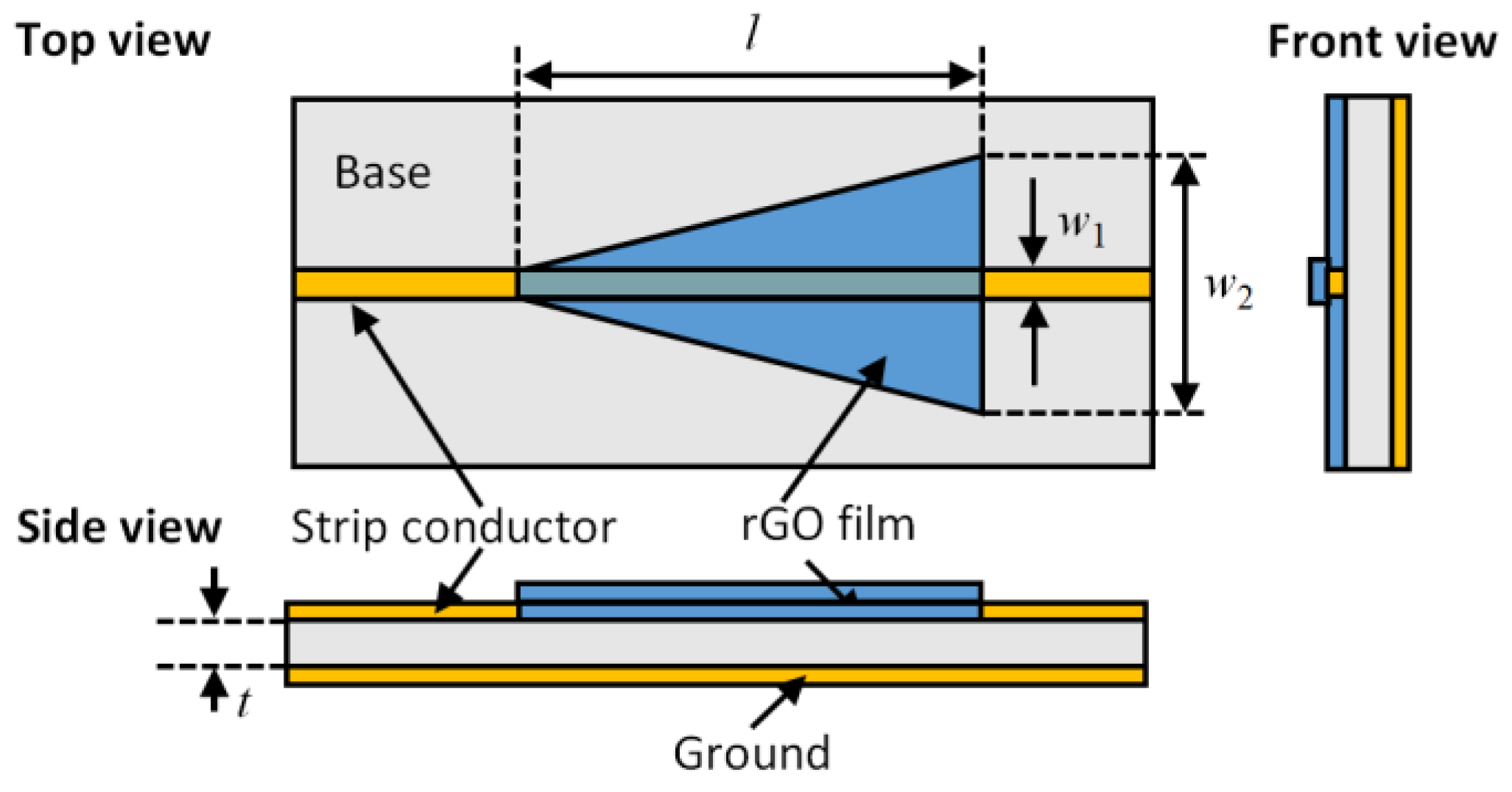
2. Structural Design

2.1. Device Structure

The termination of the signal is realized by introducing a resistive rGO film on the strip conductor of a conventional MS line, which forms a lossy transmission line structure to effectively absorb the signal, as shown in Figure 1.
On the other hand, adding resistive film typically enlarges the imaginary part of the impendence in several magnitudes and leads to a decrease in the real part. This naturally enlarges the impendence mismatch and therefore enlarges the reflections. Therefore, the resistive film is regulated to a trapezoid shape with its width which is consistent with that (w1) of the strip conductor at the input end and gradually widens to w2 at the other end. This provides small gradual changes in impedance, as required in the small reflection theory, and is possible to shorten the length of the whole device. Table 1 lists the parameters of the trapezoid-shaped termination.

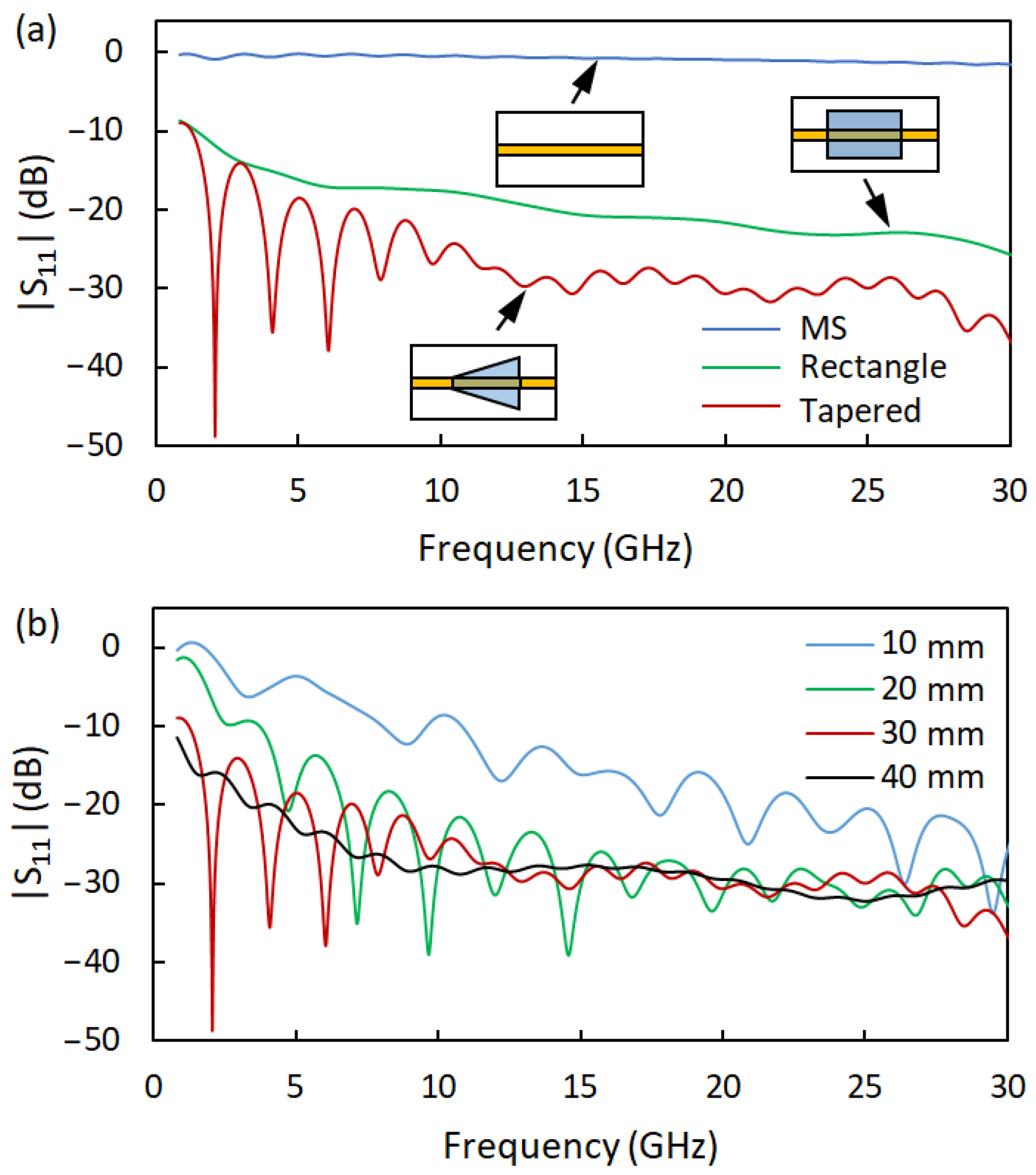
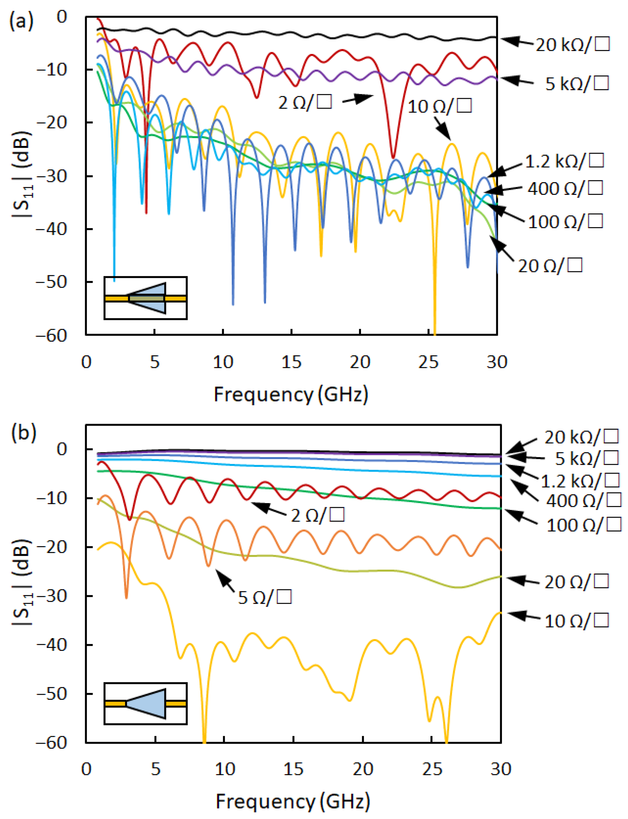
2.2. Open-End Configuration

CST Studio Suite (CST) simulations are conducted to demonstrate the radio-frequency performances of the proposed device. The return loss |S11|, which implies the reflected wave at the input port, can be determined as [21]
| S 11 | = V 1 V 1 + | V 2 + = 0
where V 1 + is the amplitude of the voltage wave incident on the input port, V 1 is the amplitude of the voltage wave reflected from the input port, and V 2 + is the amplitude of the voltage wave incident on the output port. The insertion loss |S21|, which implies the transmitted wave at the input port, can be determined as [21]
| S 21 | = V 2 V 1 + | V 2 + = 0
where V 2 is the amplitude of the voltage wave reflected from the output port.
Figure 2a shows the |S11| variations in the open-ended configuration (i.e., the RF signal inputs from the one-port while the other one keeps “open”). Firstly, the significant drops of |S11| for the samples with rectangle and tapered cases confirm the efficiency of the attenuation through implantation of resistive films. Secondly, the decreased |S11| at higher frequencies illustrate the high-pass characteristic of the design. Thirdly, the tapered termination shows a notably lower |S11| than that in the rectangle case, approximatively 10 dB at above 11.5 GHz, demonstrating that the tapered shape is more preferred for the termination propose.
Additionally, the length of the resistive film should be considered since the microwave decays exponentially along the propagation direction. In the opened configuration, the microwave signal is attenuated twice due to the reflection at the “open-end”. Therefore, the signal can be eliminated before the reflected signal reaches the input port. This can be ascertained from Figure 2b, in which the |S11| comes near to −25 dB at a resistive film length above 20 mm and above 7 GHz.
The sheet resistance of the rGO film, as shown in Figure 3a, also determines the reflection at the input port. A moderate sheet resistance leads to a typical sub −20 dB |S11| value at a higher frequency. On the other hand, the over-large sheet resistance of 20 kΩ/□, or small sheet resistance from 2 Ω/□ to 10 Ω/□, leads to a tremendous increase in reflection to over −7 dB, due to both insufficient attenuation and impendence mismatch at the discontinuities.
Note that, for our design with an overlapped resistive film and the strip conductor, the sheet resistance can be varied in two orders of magnitude, ranging from 10 Ω/□ to 1.2 kΩ/□, with low reflections. However, this range is small for termination without the overlapped strip conductor, as shown in Figure 3b. For the latter case, the sheet resistance can be chosen only in a narrow range of around 10 Ω/□. Hence, our design with an overlapped structure does not need a strict fabrication process that produces the resistive film with a certain sheet resistance. This is possible to enhance the tolerance of fabrication errors and reduce fabrication difficulties.

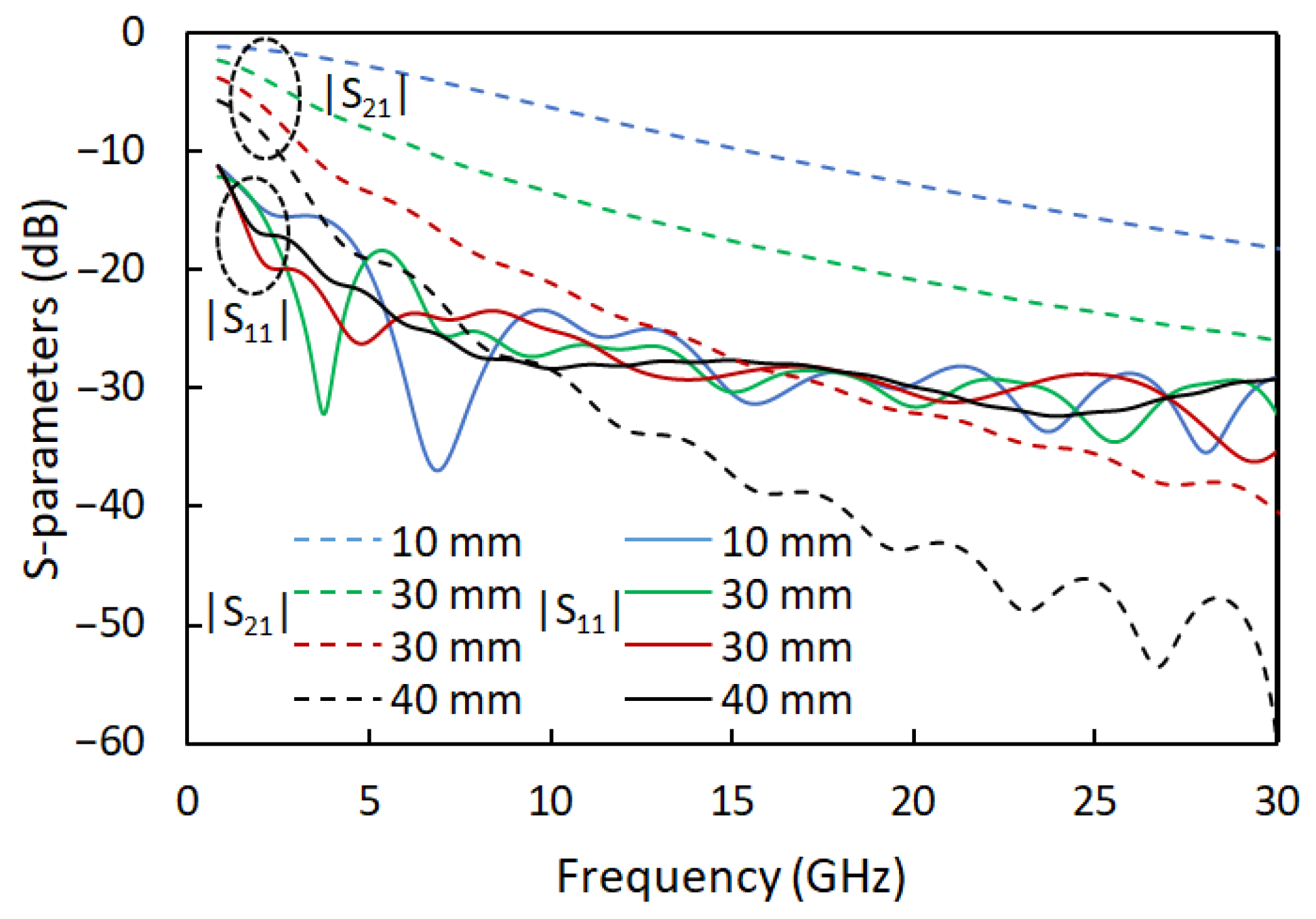
2.3. Two-Port Configuration
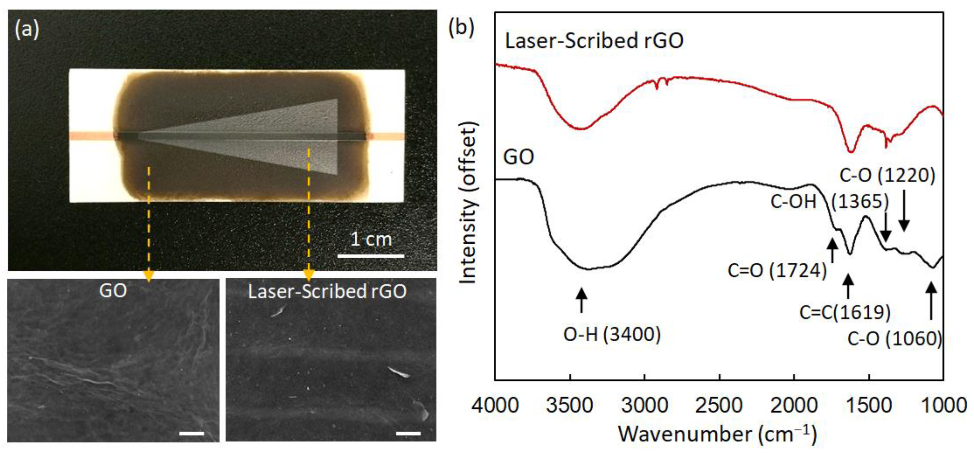
Two-port configuration is also considered to demonstrate the blockage of the transmission, as Figure 4 shows. The insertion loss |S21| illustrates a significant drop from −18 dB to over −50 dB at 30 GHz with an increasing length l from 10 mm to 40 mm. On the other hand, all four cases show a similar low|S11| level.
The S-parameters as a function of the sheet resistance are plotted in Figure 5. The sheet resistances within the range from 20 Ω/□ to 1.2 kΩ/□ provide a sub−20 dB reflection level above 5.2 GHz. The|S21|can change in a large range from a −15 dB level to a −60 dB level, accordingly. Therefore, the termination is possible for some attention applications by choosing a certain sheet resistance.

3. Fabrications

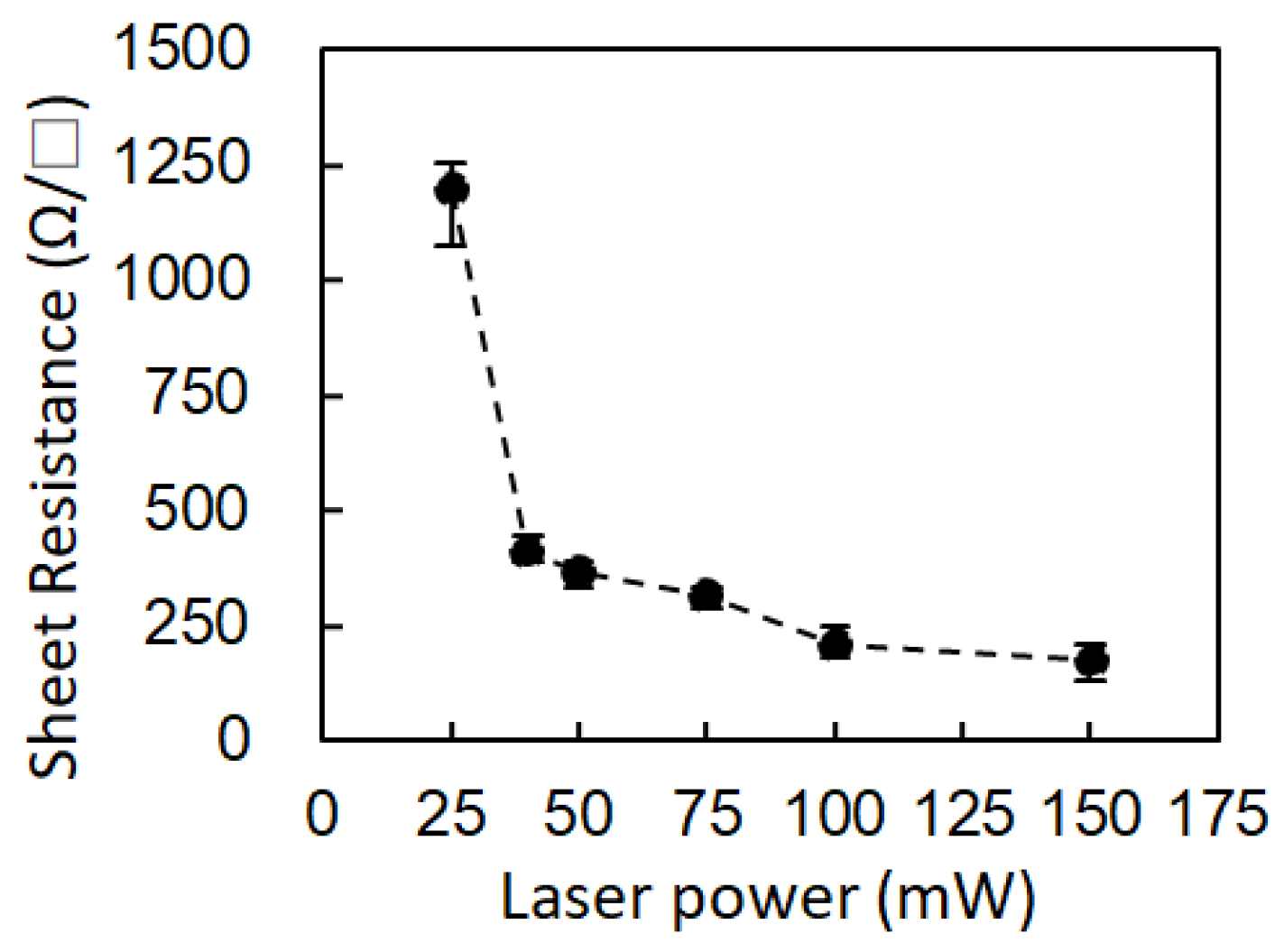
3.1. Device Fabrication

The aqueous dispersion of graphene oxide (GO) was synthesized from graphite flakes via a modified Hummers method [13] at a GO concentration of 3.5 mg/mL. For the sample preparation, the microstrip transmission lines of 5 cm in length were customized using commercial copper-clad laminates (RO4003C, thickness: 0.508 mm, Rogers Corporation). Then, the GO dispersion was spread onto the microstrip samples and dried on a hot plate at 50 °C in an ambient atmosphere. The areal density of GO was 0.5 mg/cm2.
To transfer GO film to rGO film resistor, laser direct writing was conducted using a 532 nm continuous wave laser with a typical laser power of 45 mW. The laser beam was focused onto the GO film surface through a laser focus lens (GCO-150111, 25 mm focal length, Daheng Optics, Beijing, China). The spot size was about 100 μm. A motorized platform moved the samples at a typical writing speed of 2 mm/s and a 50 μm sweep spacing to pattern the GO film.

3.2. Characterization

The morphology and microstructures were characterized by a scanning electron microscope (SEM, Gemini500, ZEISS Microscopy, Jena, Germany). The Fourier transform infrared spectroscopy (FTIR) spectra were obtained using a Nicolet Nexus 670 FTIR spectrometerr (Thermo Electron Corporation, Madison, WI, USA). The sheet resistance was obtained from the formula Rs = Rw/l, where the resistance R was measured using a source meter (2400 SourceMeter, Keithley Instruments, Cleveland, OH, USA), and w and l are the width and length of the electrode, respectively. The RF performance of the terminal was examined by a vector network analyzer (ZVA67, Rohde & Schwarz, Muenchen, Germany) from 0.2 GHz to 30 GHz.

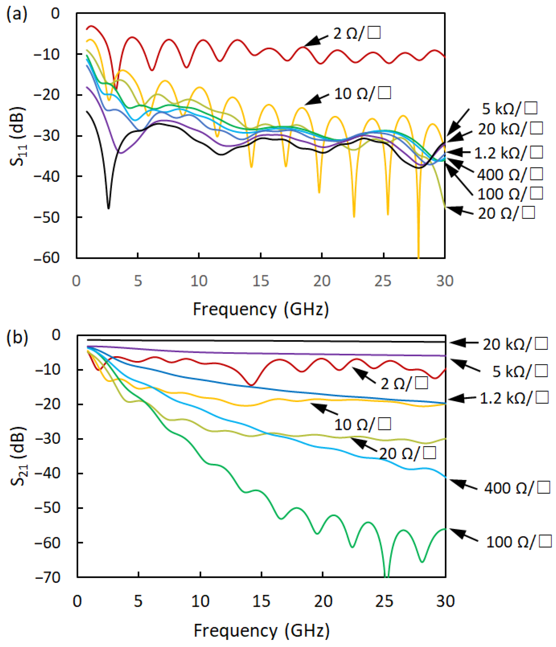
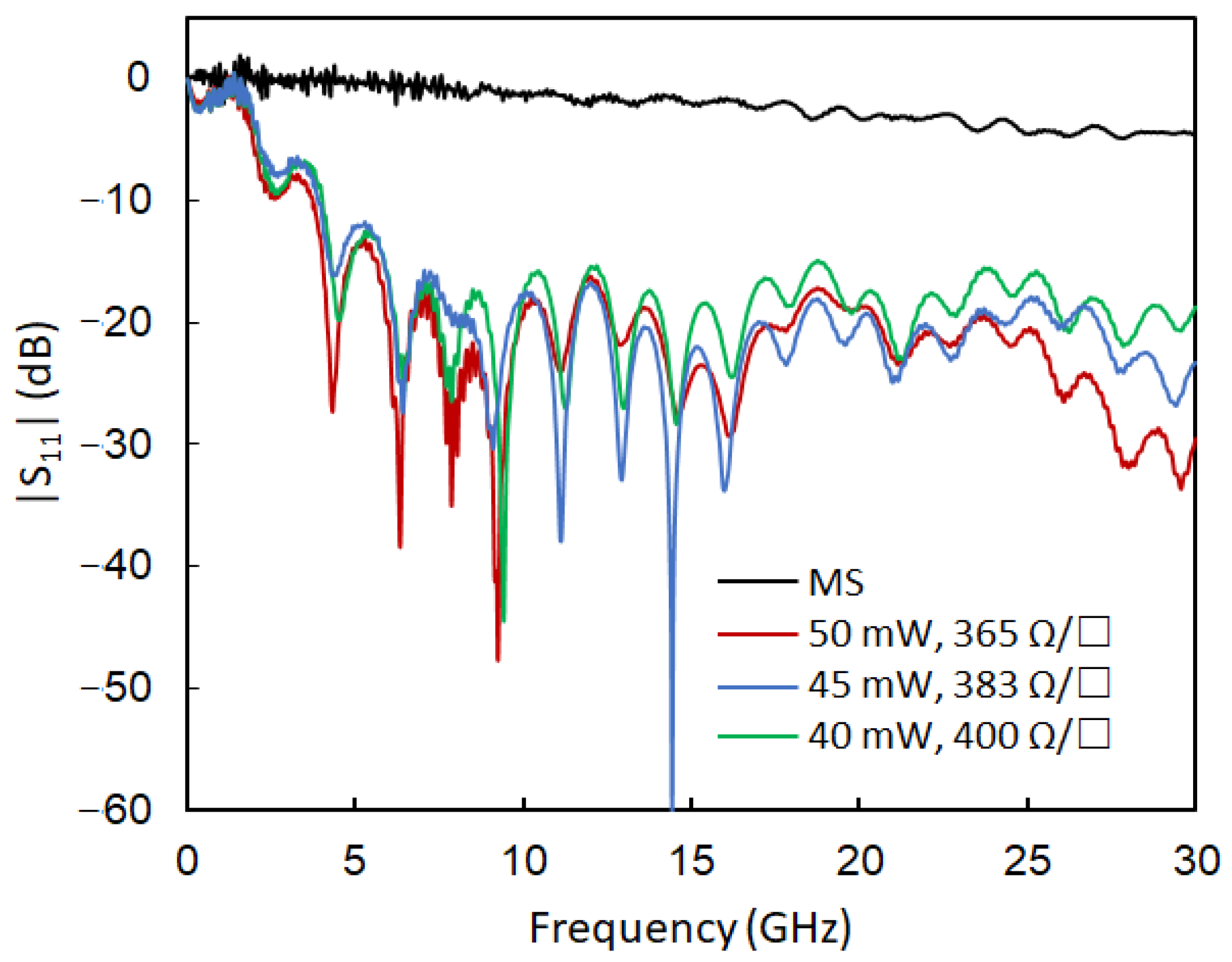
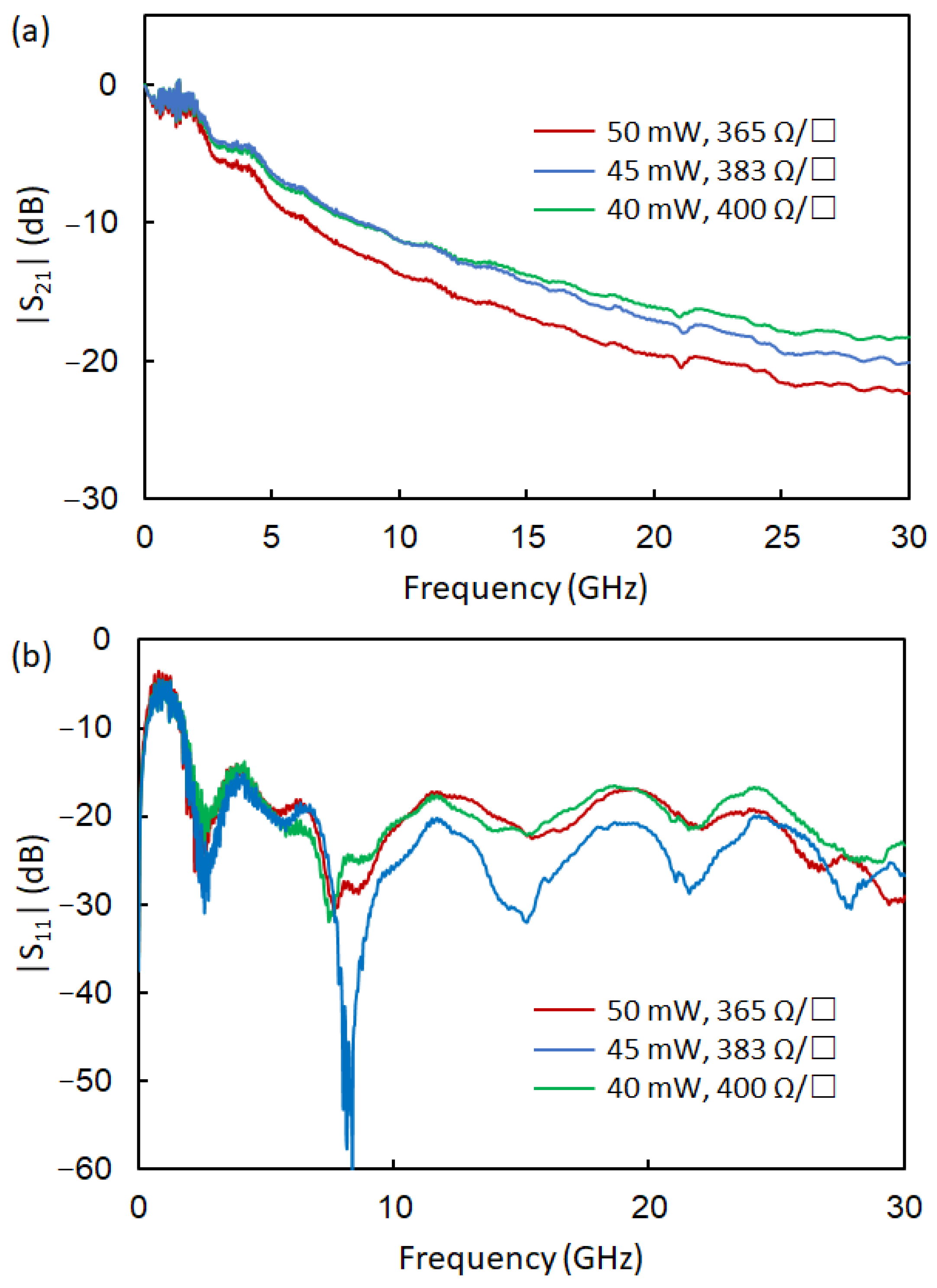
4. Results and Discussions

The laser-scripted open-end termination is demonstrated in Figure 6a. As investigated in the previous studies [13], laser irradiation of graphene oxide film turns its color from brown to metallic grey, which implies the formation of rGO. The insets demonstrate the scanning electron microscope images of the GO and laser-scribed rGO film.
During the continuous wave laser irradiation, the single-photon absorption produces a photothermal effect with a strong heat accumulation, leading to an increase in temperature at the vicinity of the focal point. This enables photothermal reduction, where the oxygen-containing groups mounted on the GO sheets are removed via thermal decomposition [22], as the FTIR spectra presents in Figure 6b. The GO spectrum shows several characteristic peaks which are attributed to the epoxide, hydroxyl, and carboxylic groups [23]. The peak at 1619 cm−1 corresponds to the vibration of aromatic C=C bonds. The broadband around 3380 cm−1 is due to the stretching vibration of the O-H. The peak at 1724 cm−1 is assigned to the C=O stretching vibration, and the peaks at 1060 cm−1 and 1220 cm−1 are attributed to the C-O stretch vibrations. Obviously, the peak strength of the oxygen-containing groups is weakened for the laser-scribed rGO.
As the result, the C/O ratio is gradually increased from 2.09 to 4.06 with increased laser power, as we previously reported [13], whereas the oxygen concentration decreases. By tuning the laser reduction degree, the oxygen content could be tuned, thus the conductivity of the rGO film could also be changed within a certain range.
The sheet resistance was obtained from the formula Rs = Rw/l, where the resistance R was measured using a Keithley 2400 source meter, and w and l are the width and length of the electrode, respectively. The measured sheet resistances are plotted in Figure 7, illustrating a tunable feature from around 1.2 kΩ/□ to 175 Ω/□ with increasing laser power. The corresponding conductivity ranges from 75.4 S/m to 517 S/m, which is obviously lower than that of silver-based conductors (>103 S/m) [24]. Note that the laser scripted rGO film provides a well-matched sheet-resistance range to the device design (20 Ω/□~1.2 kΩ/□) for the goal of high absorption and low reflection. Therefore, a wide laser power range from 25 mW to 150 mW can be chosen for the LDW. The thin GO film without laser irradiation illustrates a very low conductivity, which is similar to a dielectric. The influences of the remaining GO on the S-parameters can be ignored.
The fabricated terminations were examined by a vector network analyzer (ZVA67, Rohde & Schwarz) from 0.2 GHz to 30 GHz. A variation of the laser power from 40 mW to 50 mW was demonstrated by three samples with corresponding sheet resistances of 410 Ω/□, 383 Ω/□, and 365 Ω/□, respectively, simulating the fabrication-error-caused variations of the sheet resistance. The measured reflections (|S11|) in Figure 8 show high return losses. All samples provide a termination level of over −10 dB at frequencies above 4.0 GHz, and a terminal level of over −15 dB at frequencies above 6.0 GHz. This confirms the efficacy of the design and the fabrication process, and the functionality of the resulting terminations.
Additionally, the S-parameters of the laser-scribed termination at two-port configurations is measured, as plotted in Figure 9. The terminations can provide over a −10 dB attenuation level (|S21|) at frequencies above 8.5 GHz. The reflection level is low as <−10 dB at frequencies above 1.7 GHz and <−15 dB at frequencies above 2.0 GHz. Thus, the laser-scribed termination is a possible application for attenuation purposes.

5. Conclusions

In this article, we proposed a tapered open-end termination design with an overlapped lossy resistive rGO film and a strip conductor. This design provides a well-matched sheet-resistance range between device design (20 Ω/□~1.2 kΩ/□) and laser-scripted rGO (175 Ω/□~1.2 kΩ/□ with 150 mW~25 mW laser power, respectively). The large sheet-resistance range can also reduce the fabrication difficulties and give more choices of materials. The fabricated termination provides broadband absorption for high frequencies, with a return loss of >−15 dB at above 6.0 GHz. The termination can also be used for attenuation over a −10 dB attenuation level (>8.5 GHz) with a low reflection level better than −15 dB (>2.0 GHz). Moreover, the laser-direct writing-based technique enables fast prototyping or modification, which promotes flexible and low-cost manufacturing and will be beneficial for device design.

Author Contributions

R.-Z.L. and J.Y. conceived and designed the experiments; R.-Z.L., X.Y. and Z.W. performed the simulations; Y.Y. analyzed the data; and J.J. contributed materials. R.-Z.L. and Y.F. wrote the manuscript. All authors have read and agreed to the published version of the manuscript.

Funding

This research was funded by the National Natural Science Foundation of China (61704090, 11904177), the Natural Science Foundation of Jiangsu Province (BK20170908, BK20170903).

Conflicts of Interest

The authors declare no conflict of interest.

References

  1. Morimoto, Y.; Memarian, M.; Li, X.; Itoh, T. Open-End Microstrip Line Terminations Using Lossy Gray-Scale Inkjet Printing. IEEE Trans. Microw. Theory Tech. 2017, 65, 4861–4870. [Google Scholar] [CrossRef]
  2. Lopez-Berrocal, B.; de-Oliva-Rubio, J.; Molina-Fernandez, I. Design and implementation of DC–20-GHz lumped resistor matched loads for planar microwave circuits. IEEE Trans. Microw. Theory Tech. 2009, 57, 2439–2443. [Google Scholar] [CrossRef]
  3. Dummer, M.M.; Sysak, M.N.; Tauke-Pedretti, A.; Raring, J.W.; Klamkin, J.; Coldren, L.A. Widely tunable separate absorption and modulation wavelength converter with integrated microwave termination. J. Lightwave Technol. 2008, 26, 938–944. [Google Scholar] [CrossRef]
  4. Arbaoui, Y.; Laur, V.; Maalouf, A.; Queffelec, P.; Passerieux, D.; Delias, A.; Blondy, P. Full 3-D printed microwave termination: A simple and low-cost solution. IEEE Trans. Microw. Theory Tech. 2015, 64, 271–278. [Google Scholar] [CrossRef]
  5. Lacombe, D. A Multioctave Microstrip 50-Ω Termination (Short Papers). IEEE Trans. Microw. Theory Tech. 1972, 20, 290–292. [Google Scholar] [CrossRef]
  6. Linner, L.; Lunden, H.B. Theory and design of broad-band nongrounded matched loads for planar circuits (short paper). IEEE Trans. Microw. Theory Tech. 1986, 34, 892–896. [Google Scholar] [CrossRef]
  7. Giannini, F.; Paoloni, C.; Ruggieri, M. A very broadband matched termination utilizing non-grounded radial lines. In Proceedings of the 1987 17th European Microwave Conference, Rome, Italy, 4–6 October 1987; pp. 1027–1031. [Google Scholar]
  8. Shu, M.; Guo, C.; Shang, X.; Zhu, W.; Zhang, A. A Ka-Band Wideband Matched Load Based on Lossy Waveguide Structures. IEEE Microw. Wirel. Compents 2020, 30, 1045–1048. [Google Scholar] [CrossRef]
  9. Lomakin, K.; Sippel, M.; Gold, G.; Froehlich, J.; Helmreich, K.; Ankenbrand, M.; Franke, J. Low reflective aerosol jet printed broadband matched load up to 67 GHz. In Proceedings of the 2018 11th German Microwave Conference (GeMiC), Freiburg, Germany, 12–14 March 2018; pp. 379–382. [Google Scholar]
  10. Hu, A.; Li, R.; Bridges, D.; Zhou, W.; Bai, S.; Ma, D.; Peng, P. Photonic nanomanufacturing of high performance energy devices on flexible substrates. J. Laser Appl. 2016, 28, 022602. [Google Scholar] [CrossRef]
  11. Yu, Y.; Wang, S.; Ma, D.; Joshi, P.; Hu, A. Recent Progress on Laser Manufacturing of Microsize Energy Devices on Flexible Substrates. JOM 2018, 70, 1816–1822. [Google Scholar] [CrossRef]
  12. Zhou, X.; Guo, W.; Zhu, Y.; Peng, P. The laser writing of highly conductive and anti-oxidative copper structures in liquid. Nanoscale 2020, 12, 563–571. [Google Scholar] [CrossRef]
  13. Li, R.-Z.; Peng, R.; Kihm, K.; Bai, S.; Bridges, D.; Tumuluri, U.; Wu, Z.; Zhang, T.; Compagnini, G.; Feng, Z. High-rate in-plane micro-supercapacitors scribed onto photo paper using in situ femtolaser-reduced graphene oxide/Au nanoparticle microelectrodes. Energy Environ. Sci. 2016, 9, 1458–1467. [Google Scholar] [CrossRef]
  14. El-Kady, M.F.; Strong, V.; Dubin, S.; Kaner, R.B. Laser scribing of high-performance and flexible graphene-based electrochemical capacitors. Science 2012, 335, 1326–1330. [Google Scholar] [CrossRef] [PubMed] [Green Version]
  15. Gao, W.; Singh, N.; Song, L.; Liu, Z.; Reddy, A.L.; Ci, L.; Vajtai, R.; Zhang, Q.; Wei, B.; Ajayan, P.M. Direct laser writing of micro-supercapacitors on hydrated graphite oxide films. Nat. Nanotechnol. 2011, 6, 496–500. [Google Scholar] [CrossRef] [PubMed]
  16. Cheng, C.; Wang, S.; Wu, J.; Yu, Y.; Li, R.; Eda, S.; Chen, J.; Feng, G.; Lawrie, B.; Hu, A. Bisphenol A Sensors on Polyimide Fabricated by Laser Direct Writing for Onsite River Water Monitoring at Attomolar Concentration. ACS Appl. Mater. Interfaces 2016, 8, 17784–17792. [Google Scholar] [CrossRef] [PubMed]
  17. Li, Y.; Zhou, X.; Chen, J.; Guo, W.; He, S.; Gao, S.; Peng, P. Laser-Patterned Copper Electrodes for Proximity and Tactile Sensors. Adv. Mater. Interfaces 2020, 7, 1901845. [Google Scholar] [CrossRef]
  18. Li, R.; Yan, J.; Fang, Y.; Fan, X.; Sheng, L.; Ding, D.; Yin, X.; Yu, Y. Laser-Scribed Lossy Microstrip Lines for Radio Frequency Applications. Appl. Sci. 2019, 9, 415. [Google Scholar] [CrossRef] [Green Version]
  19. Peng, P.; Li, L.; He, P.; Zhu, Y.; Fu, J.; Huang, Y.; Guo, W. One-step selective laser patterning of copper/graphene flexible electrodes. Nanotechnology 2019, 30, 185301. [Google Scholar] [CrossRef] [PubMed]
  20. Hong, J.-S.G.; Lancaster, M.J. Microstrip Filters for RF/Microwave Applications; John Wiley & Sons: Hoboken, NJ, USA, 2004; Volume 167. [Google Scholar]
  21. Pozar, D.M. Microwave Engineering; John Wiley & Sons: Hoboken, NJ, USA, 2011. [Google Scholar]
  22. Sygellou, L.; Paterakis, G.; Galiotis, C.; Tasis, D. Work Function Tuning of Reduced Graphene Oxide Thin Films. J. Phys. Chem. C 2016, 120, 281–290. [Google Scholar] [CrossRef]
  23. Xie, Q.; Zhang, S.; Xiao, Z.; Hu, X.; Hong, Z.; Yi, R.; Shao, W.; Wang, Q. Preparation and characterization of novel alkali-resistant nanofiltration membranes with enhanced permeation and antifouling properties: The effects of functionalized graphene nanosheets. RSC Adv. 2017, 7, 18755–18764. [Google Scholar] [CrossRef] [Green Version]
  24. Dionigi, M.; Tomassoni, C.; Venanzoni, G.; Sorrentino, R. Simple High-Performance Metal-Plating Procedure for Stereolithographically 3-D-Printed Waveguide Components. IEEE Microw. Wirel. Compents 2017, 27, 953–955. [Google Scholar] [CrossRef]
Figure 1. Illustration diagrams of the laser-scribed termination.
Applsci 11 06960 g001
Figure 2. (a) Calculated |S11| of the laser-scribed tapered termination, rectangle termination, and the microstrip (MS) line. (b) Calculated |S11| with a series of resistive film lengths. (a) Calculated |S11| of the laser-scribed tapered termination, rectangle termination, and the microstrip (MS) line. (b) Calculated |S11| with a series of resistive film lengths.
Applsci 11 06960 g002
Figure 3. The S-parameters of the laser-scribed terminations with a series of sheet resistances of rGO film in the case of (a) an overlapped structure with copper strip conductors in the center, and (b) a design without copper strip conductors.
Applsci 11 06960 g003
Figure 4. The S-parameters of the laser-scribed terminations with a series of rGO lengths l in two-port configurations.
Applsci 11 06960 g004
Figure 5. The S-parameters of the terminations as a function of the sheet resistance of rGO at double-end configurations, (a) reflections |S11|, and (b) transmissions |S21|.
Applsci 11 06960 g005
Figure 6. (a) Laser-scripted open-end termination. The insets are the scanning electron microscope (SEM) images of the GO and laser-scribed rGO film with a laser power of 40 mW. The scale bar indicates 20 μm. (b) the Fourier transform infrared spectroscopy (FTIR) spectra of the GO and laser-scribed rGO film.
Applsci 11 06960 g006
Figure 7. The sheet resistance of the laser-scripted rGO resistive film as a function of laser power.
Applsci 11 06960 g007
Figure 8. The measured |S11| of the laser-scribed terminations.
Applsci 11 06960 g008
Figure 9. The measured S-parameters of the laser-scribed termination at two-port configurations, (a) transmissions |S21| and (b) reflections |S11|.
Applsci 11 06960 g009
Table 1. The parameters of the termination.
ParametersValue
Width of the strip conductor, w11.15 mm
Width of the rGO resistive film, w211.70 mm
Length of the rGO resistive film, l30 mm
Thickness of the dielectric substrate, t0.508 mm
Thickness of the rGO film resistor, tr10 μm
Publisher’s Note: MDPI stays neutral with regard to jurisdictional claims in published maps and institutional affiliations.

