
Energy-Efficient Word-Serial Processor for Field Multiplication and Squaring Suitable for Lightweight Authentication Schemes in RFID-Based IoT Applications


Abstract
:1. Introduction
1.1. Motivation
1.2. Contribution
- We developed the bit-level version of the bipartite multiplication and squaring algorithm to have its regular iterative form;
- We obtained the DG of the developed algorithm to help in extracting the unified hardware module;
- We obtained a nonlinear scheduling function to allocate a time value to each node of the DG;
- We developed a nonlinear projection function to map the DG nodes to the corresponding Processing Element (PE) in the extracted processor core.
1.3. Paper Organization
2. Related Work
3. Polynomial-Based Bipartite Multiplication-Squaring Algorithm over GF(2n)
| Algorithm 1 Bipartite multiplication and squaring algorithm in GF(). |
| Input: , ∈ GF(), , , , and Mult. Output: Square Output: Initialization: Algorithm:
|
| Algorithm 2 Bit-level form of the bipartite multiplication and squaring algorithm. |
| Input: , ∈ GF(), , , , and Mult. Output: Square Output: Initialization: Algorithm:
|
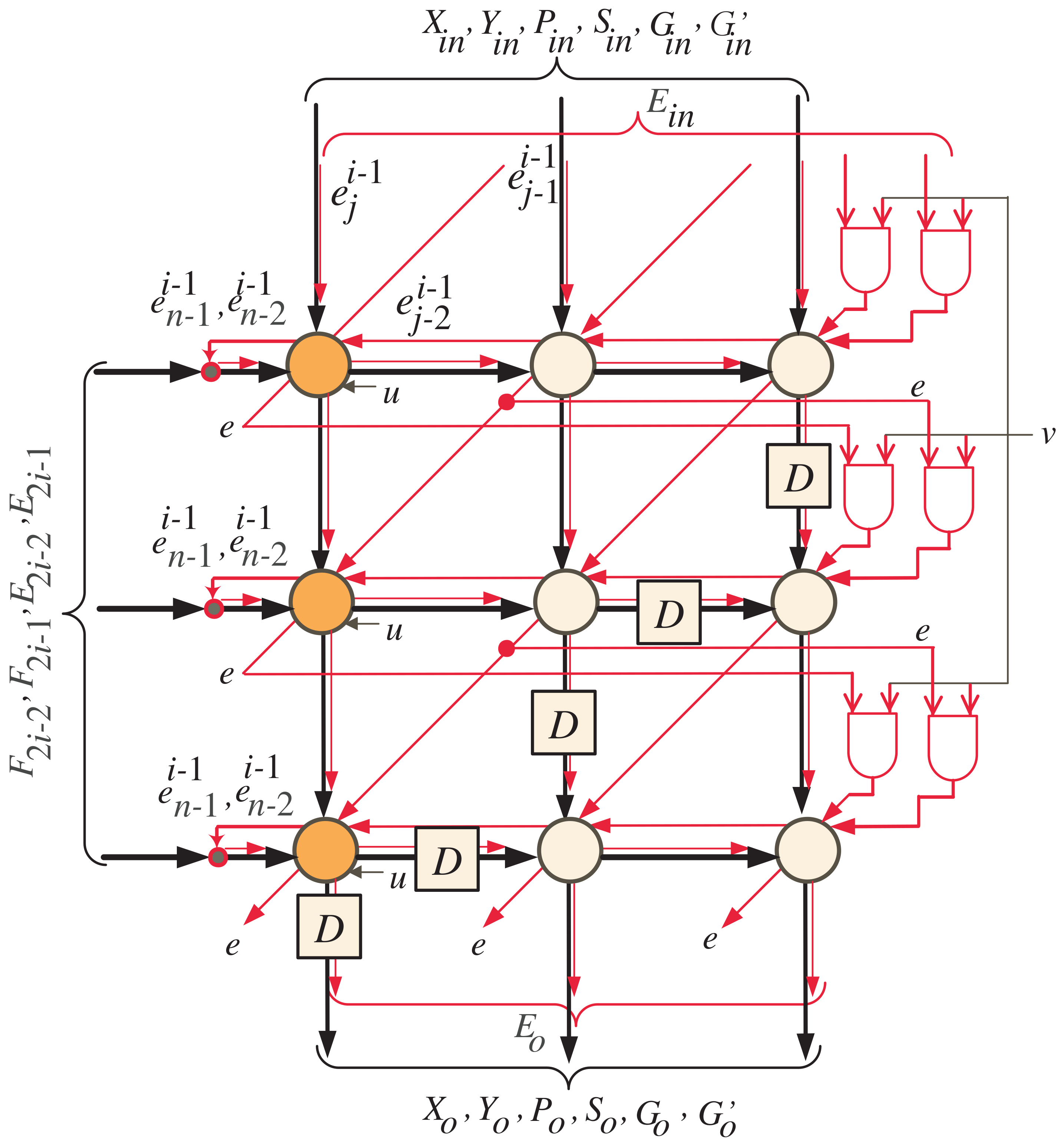
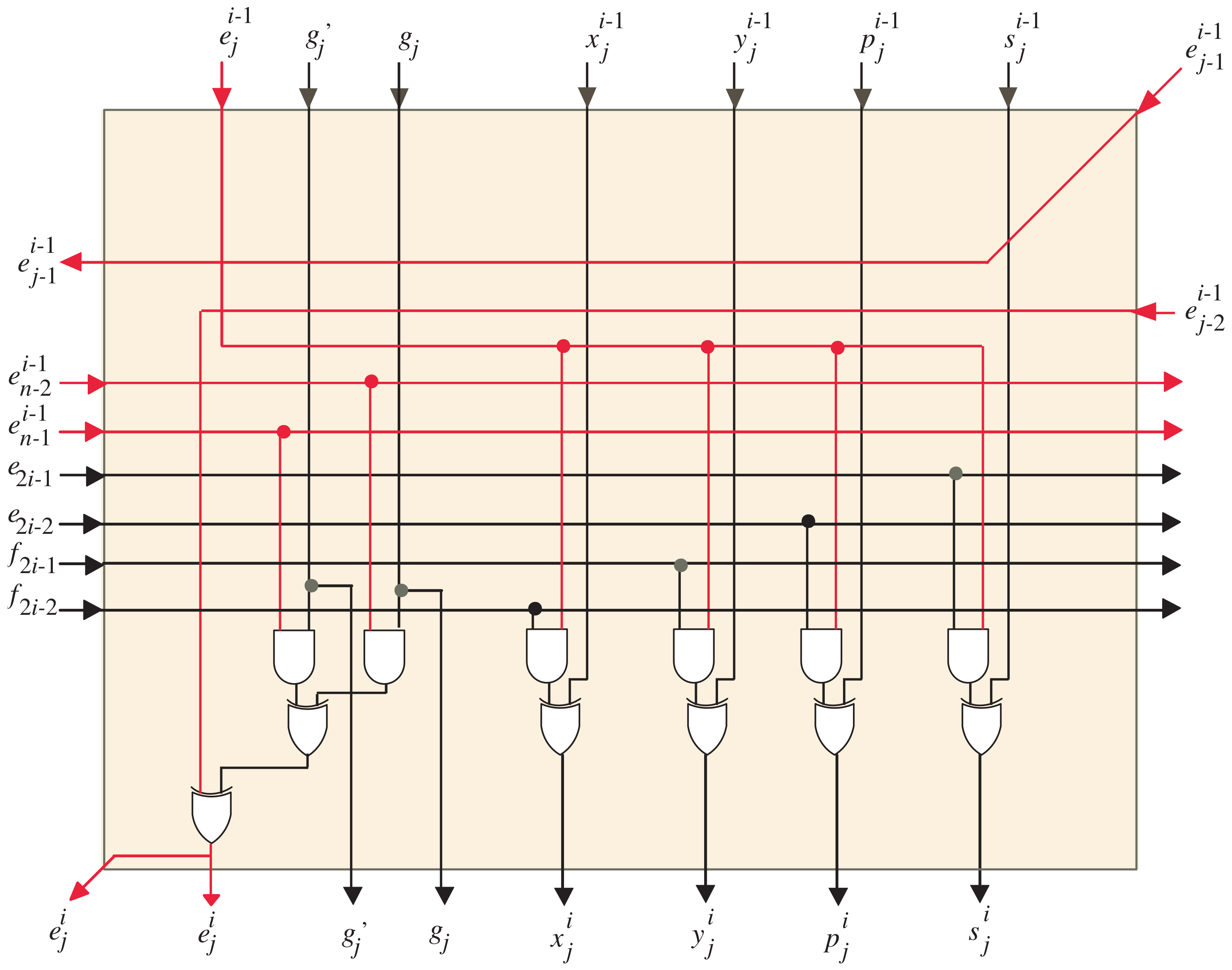
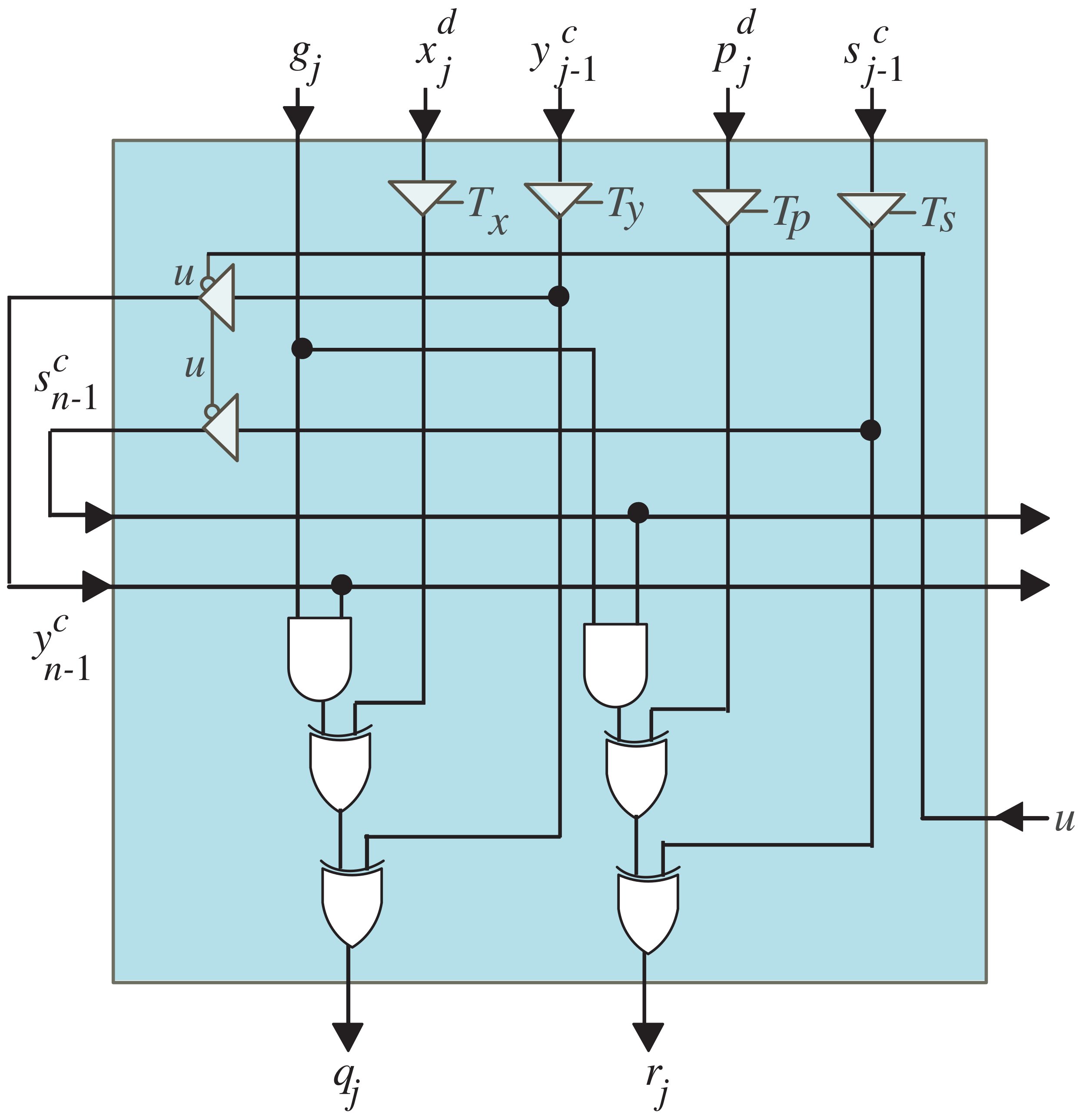
4. Extraction of the Word-Based SISO Semisystolic Processor
- The inputs and outputs can only be accessed as bit-serial (one bit at a time) or bit-parallel (all bits at the same time instance) based on our choice of the scheduling function. That means that the linear functions cannot satisfy any restrictions on the processor bus size;
- The designer cannot manage the number of accessed input or output samples at a particular time step;
- The number of active PEs cannot be managed at a specific time step;
- The designer cannot manage the PE’s workload.
4.1. Word-Based SISO Scheduling Function
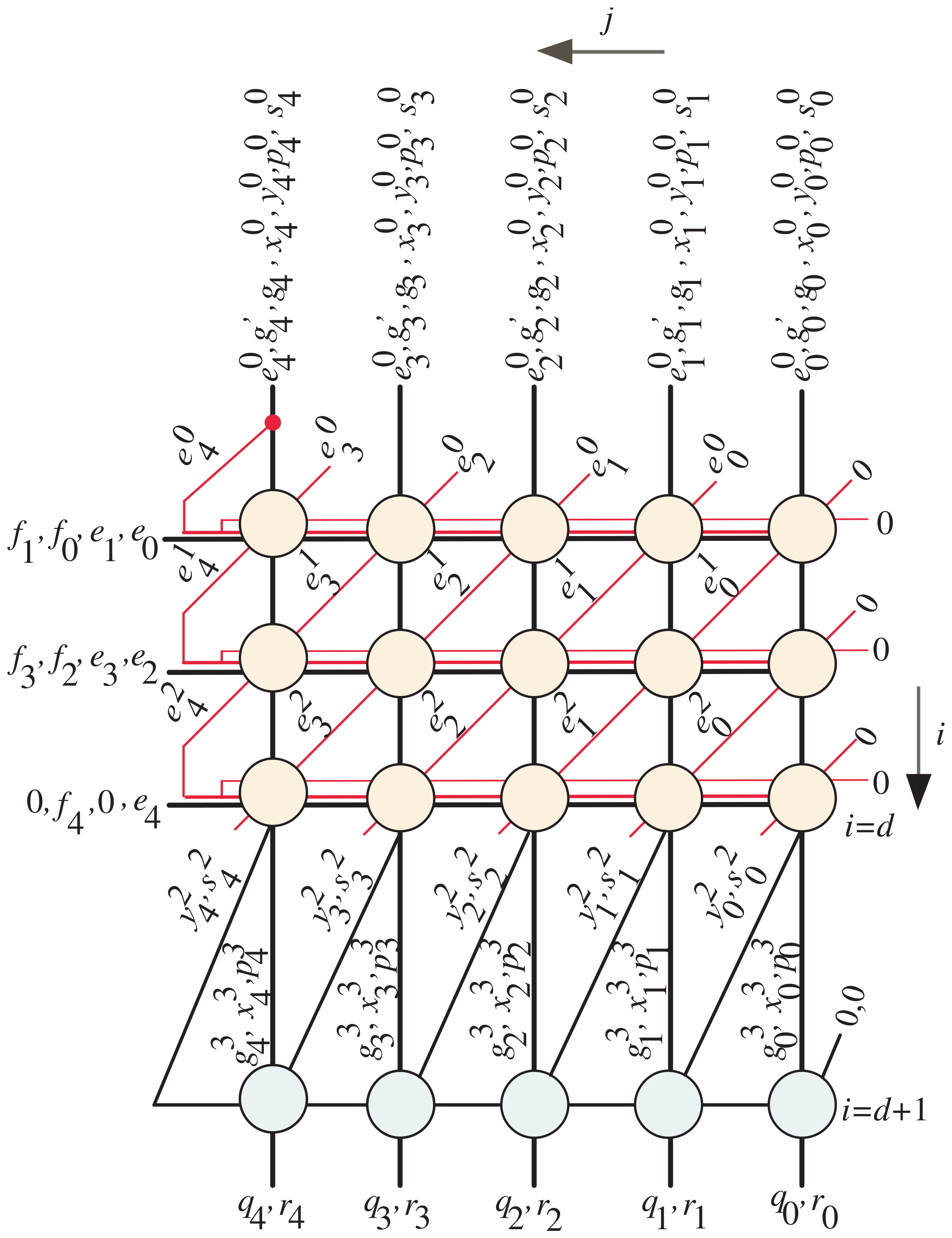
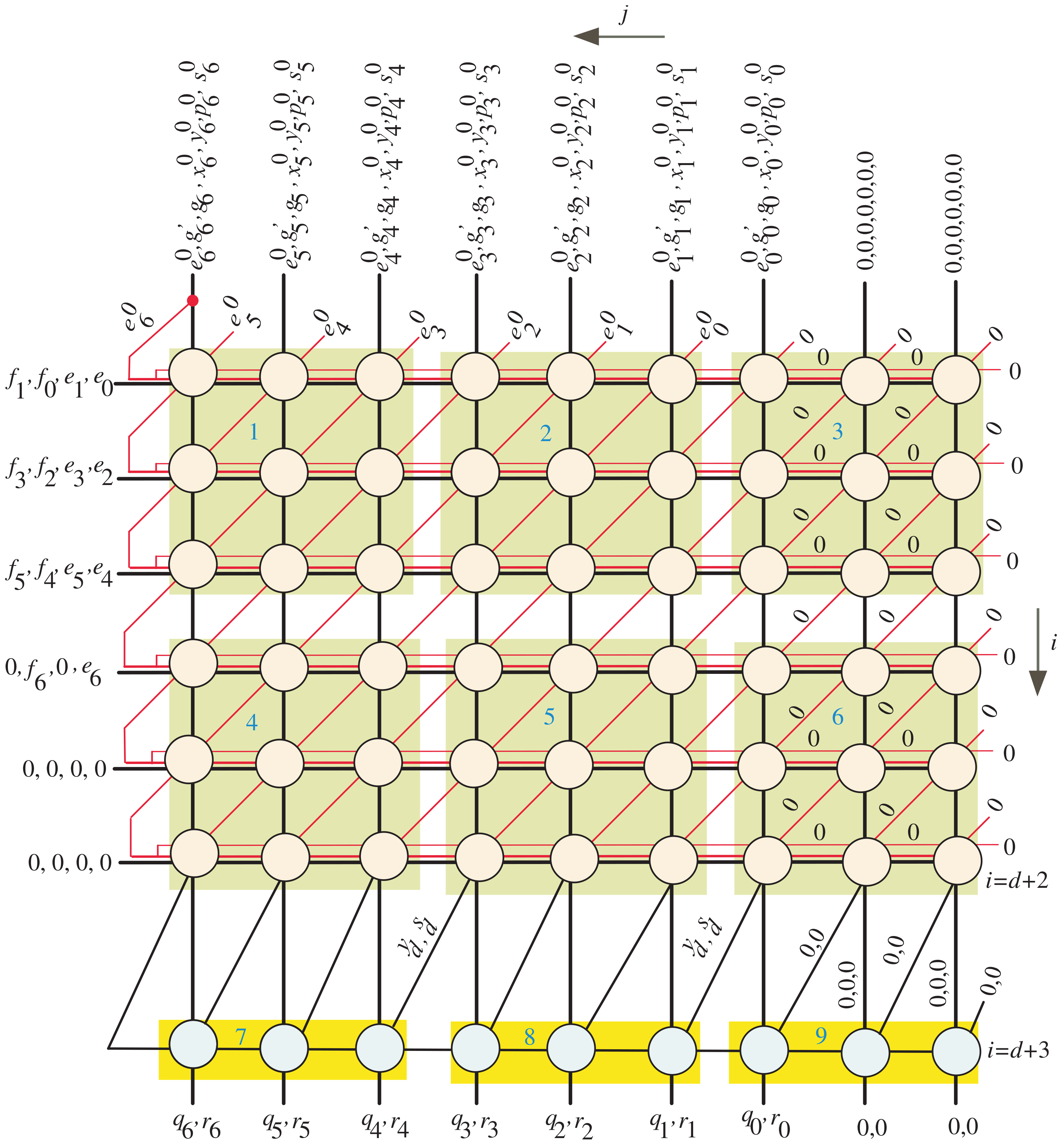
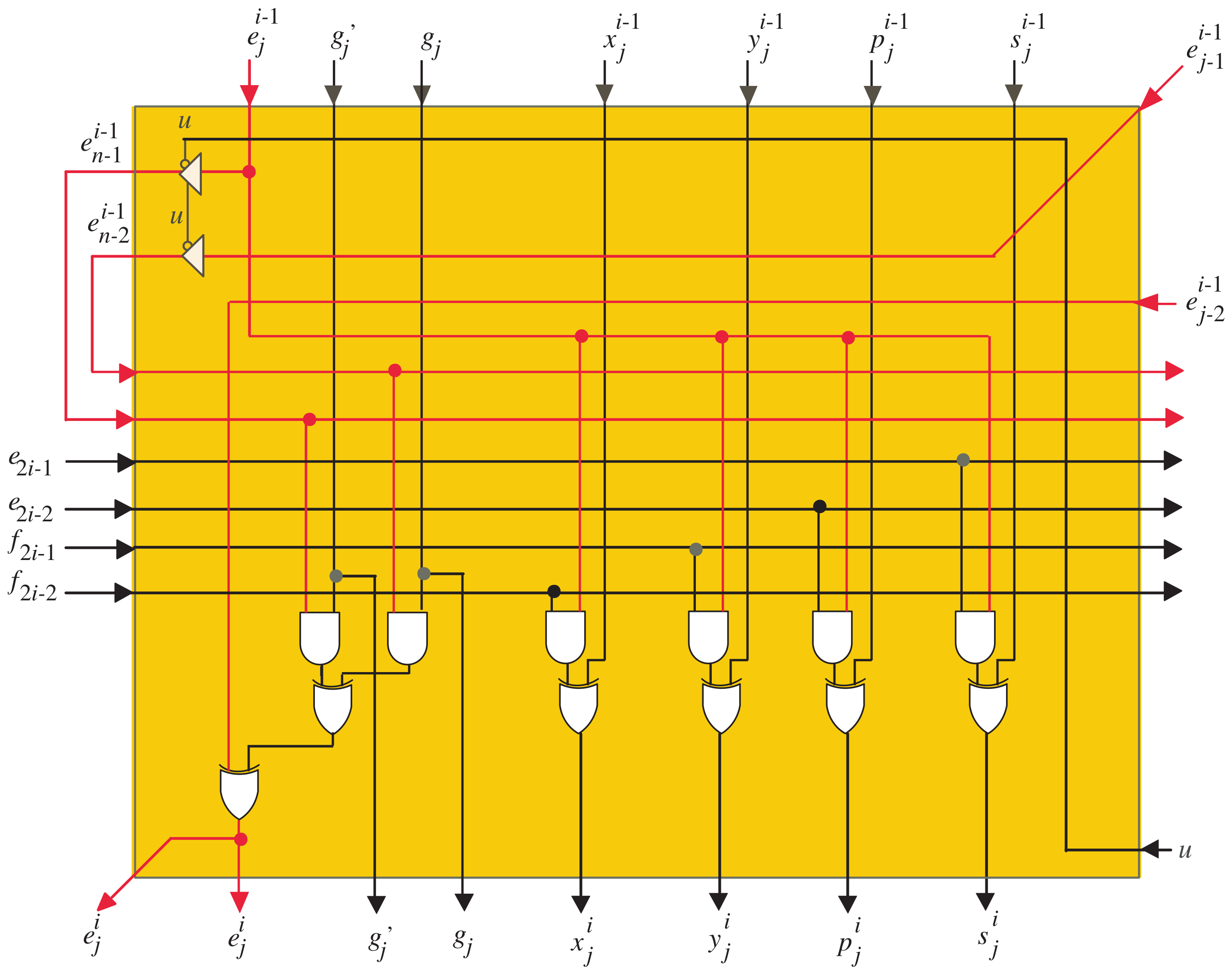
4.2. Word-Based SISO Projection Function
- Through clock periods , the control signals of MUXes , , and , presented in Figure 5, are set to one to serially transfer the words of input operands E, G, and to the corresponding inputs of the semisystolic array block (one word at each clock period) starting from the most significant words. Through the first clock period, the FIFO buffers of X, Y, P, and S are cleared to maintain zero initial values as denoted in Algorithm 1. As we notice from Figure 5, the FIFOs of X, Y, P, and S have a width size of k bits and a depth size of , where . The depth size of these buffers guarantees that the variables X, Y, P, and S have zero values through the intended clock periods, ;
- At clock periods , , the control signal u in all dark orange PEs of the semisystolic array shown in Figure 3 should be assigned a zero value () to enable the tristate buffers designated in Figure 6 to serially transfer the updated words of and to the remaining light orange PEs in the array (one word at each clock period). Furthermore, through these clock periods, the words of , , , and should be serially transferred to all the PEs in the semisystolic array. The words of , , , and are transferred to the corresponding inputs in the semisystolic array block through the registers allocated at the left side of Figure 5;
- At clock periods , , the control signal v, shown in Figure 3, should be forced to have a zero value () to force the least significant bits of E, through the AND gates, to have zero values as indicated at the rightmost edge of the DG shown in Figure 2. Notice that in our case example of and , should equal two;
- At clock periods , the control signals of MUXes , , and are assigned zero values to transfer the following words to the corresponding inputs of the semisystolic array block: updated E words saved in FIFO-E, words saved in FIFO-G’, and G words saved in FIFO-G. All of these words are transferred to the semisystolic array in a word-serial fashion (i.e., one word at each clock period). Through the same clock periods, the updated words X, Y, P, and S, saved in FIFO-X, FIFO-Y, FIFO-P, and FIFO-S, as well as the words of , , , , , and are serially passed (one word at each clock period) to the corresponding inputs of the semisystolic array block to compute serially (one word at each clock period) the intermediate partial results of X, Y, P, S, and E;
- At clock period , the control signal u in the dark blue PE of the postprocessing array, Figure 4, should be assigned a zero value () to enable the tristate buffers designated in Figure 8 to serially transfer the updated bits of and to the remaining light blue nodes of the postprocessing array. The bits of and alongside the bits , , , , and are used to determine the final words of the products Q and R;
- At clock period , the control signal v, indicated at the right side of the postprocessing array designated in Figure 4, should be forced to have a zero value () to force the least significant bits of and , through the AND gates, to have zero values as shown at the rightmost edge of the DG shown in Figure 2;
- Through clock periods , the final output words Q and R produced from the postprocessing array will be loaded serially (one word at each clock period) in registers Q and R as presented in Figure 5.
5. Experimental Results and Discussion
5.1. Analysis of the Estimated Area and Time Complexities
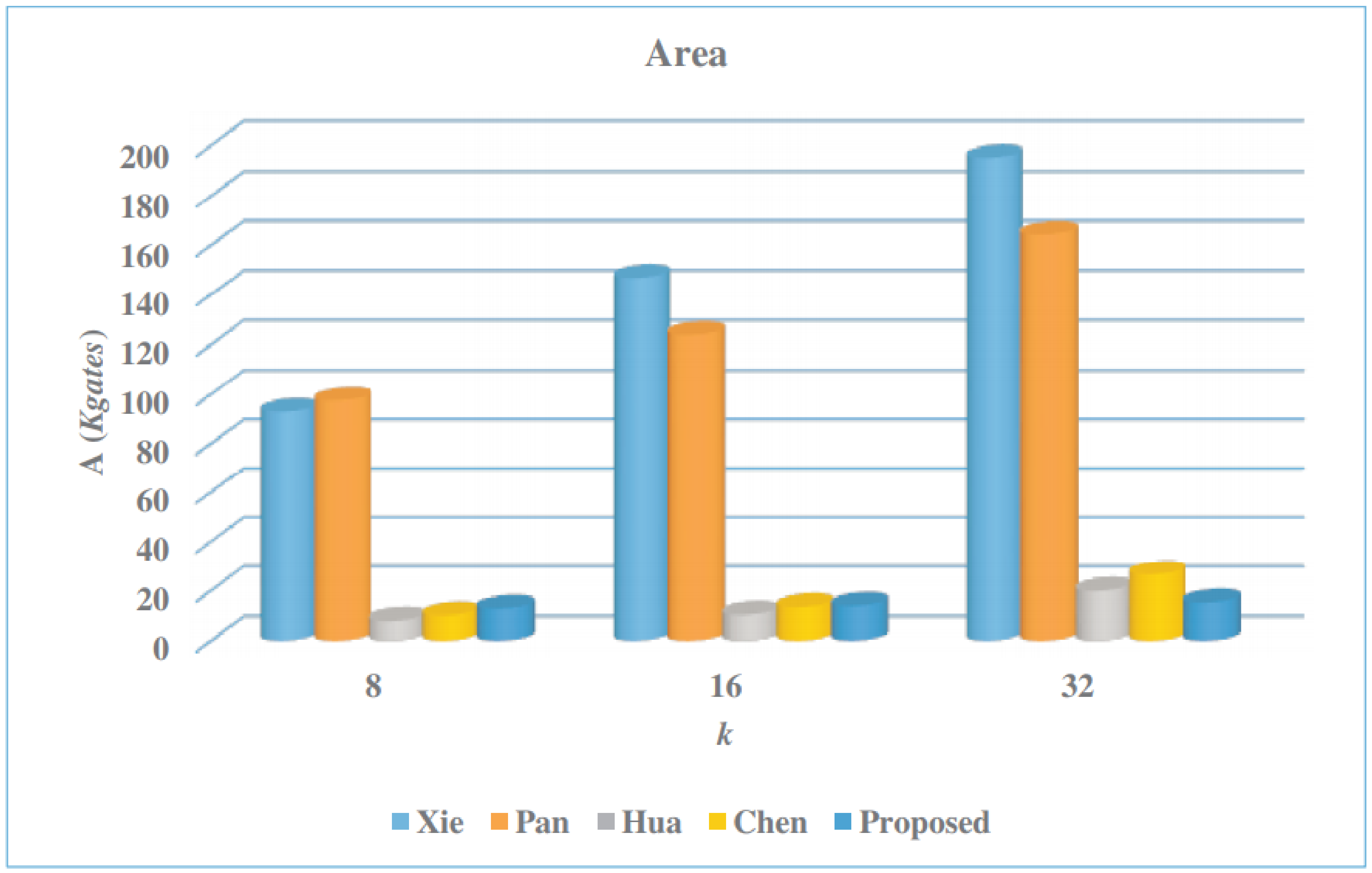
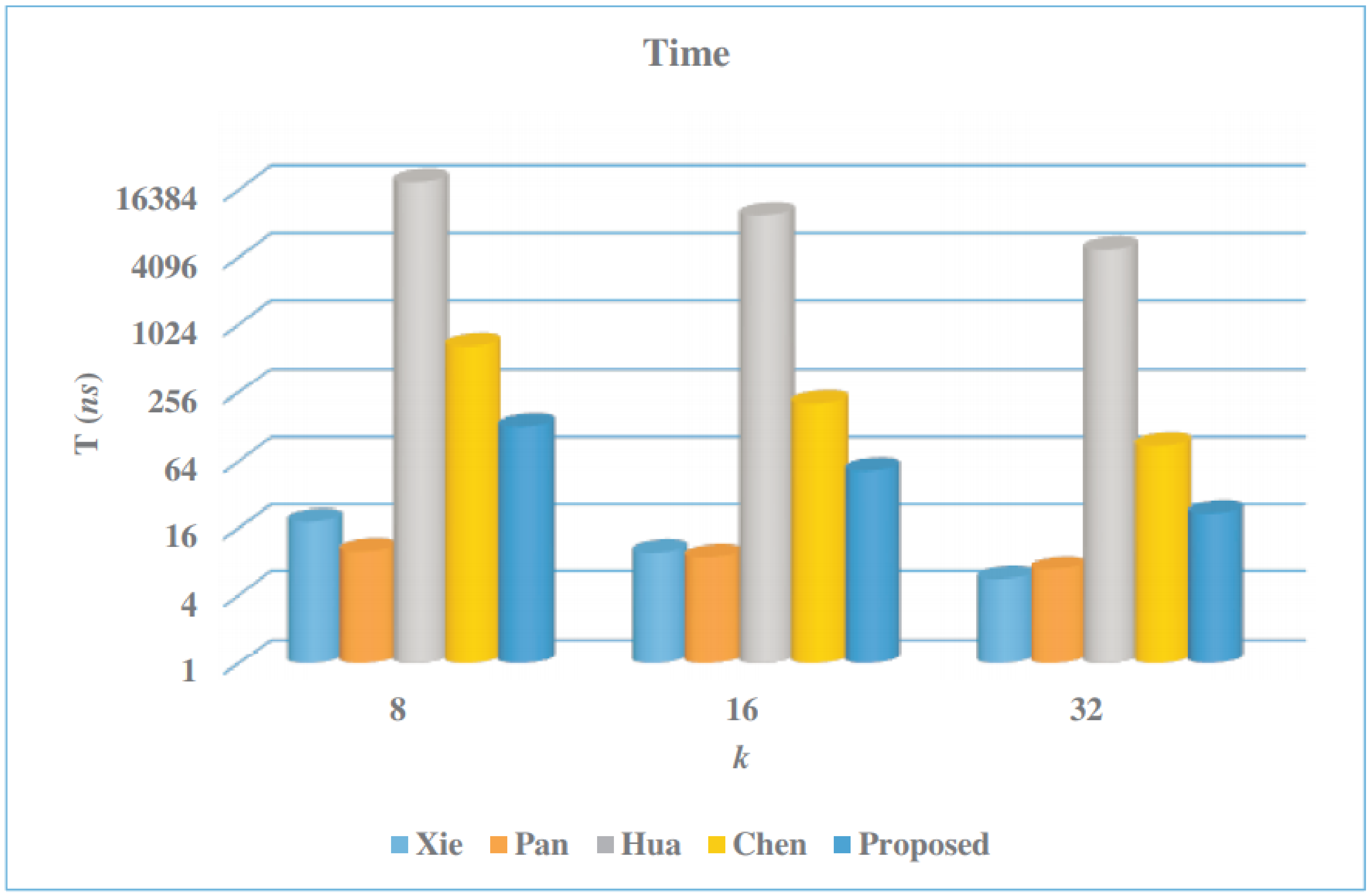
5.2. ASIC Implementation Results
- (1)
- The multiplier structure of Pan [45] achieved the lowest latency for all word sizes compared to the other structures, including the proposed one. We also observed that the latency significantly decreased, for all multiplier structures, as the word size k increased;
- (2)
- The multiplier structure of Chen [61] had the lowest CPD for all values of k.
6. Conclusions and Future Work
Author Contributions
Funding
Institutional Review Board Statement
Informed Consent Statement
Data Availability Statement
Acknowledgments
Conflicts of Interest
Abbreviations
| IoT | Internet of Things |
| RFID | Radio-Frequency Identification |
| ECC | Elliptic Curve Cryptography |
| SISO | Serial-In/Serial-Out |
| SIPO | Serial-In/Parallel-Out |
| PISO | Parallel-In/Serial-Out |
| CPD | Critical Path Delay |
| AT | Area–Time |
References
- Chen, D.; Zhang, N.; Qin, Z.; Mao, X.; Qin, Z.; Shen, X.; Li, X.Y. S2M: A lightweight acoustic fingerprints-based wireless device authentication protocol. IEEE Internet Things J. 2016, 4, 88–100. [Google Scholar] [CrossRef]
- Granjal, J.; Monteiro, E.; Silva, J.S. Security for the Internet of things: A survey of existing protocols and open research issues. IEEE Commun. Surv. Tutor. 2015, 17, 1294–1312. [Google Scholar] [CrossRef]
- Atzori, L.; Iera, A.; Morabito, G. The Internet of things: A survey. Comput. Netw. 2010, 54, 2787–2805. [Google Scholar] [CrossRef]
- Fan, K.; Gong, Y.; Liang, C.; Li, H.; Yang, Y. Lightweight and ultralightweight RFID mutual authentication protocol with cache in the reader for IoT in 5G. Secur. Commun. Netw. 2016, 9, 3095–3104. [Google Scholar] [CrossRef] [Green Version]
- Juels, A. RFID security and privacy: A research survey. IEEE J. Sel. Areas Commun. 2006, 24, 381–394. [Google Scholar] [CrossRef]
- Baashirah, R.; Abuzneid, A. Survey on prominent RFID authentication protocols for passive tags. Sensors 2018, 18, 3584. [Google Scholar] [CrossRef] [Green Version]
- Yao, W.; Chu, C.H.; Li, Z. The adoption and implementation of RFID technologies in healthcare: A literature review. J. Med. Syst. 2012, 36, 3507–3525. [Google Scholar] [CrossRef] [PubMed]
- Zhu, F.; Li, P.; Xu, H.; Wang, R. A Novel Lightweight Authentication Scheme for RFID-Based Healthcare Systems. Sensors 2020, 20, 4846. [Google Scholar] [CrossRef]
- Wu, D.L.; Wing, W.; Yeung, D.S.; Ding, H.L. A brief survey on current RFID applications. In Proceedings of the 2009 International Conference on Machine Learning and Cybernetics, Baoding, China, 12–15 July 2009; Volume 4, pp. 2330–2335. [Google Scholar]
- Kaur, M.; Sandhu, M.; Mohan, N.; Sandhu P., S. RFID technology principles, advantages, limitations & its applications. Int. J. Comput. Electr. Eng. 2011, 3, 151. [Google Scholar]
- Rahman, F.; Bhuiyan, M.Z.A.; Ahamed, S.I. A privacy preserving framework for RFID based healthcare systems. Future Gener. Comput. Syst. 2017, 72, 339–352. [Google Scholar] [CrossRef] [Green Version]
- Fan, K.; Jiang, W.; Li, H.; Yang, Y. Lightweight RFID protocol for medical privacy protection in IoT. IEEE Trans. Ind. Inform. 2018, 14, 1656–1665. [Google Scholar] [CrossRef]
- Fan, K.; Zhu, S.; Zhang, K.; Li, H.; Yang, Y. A lightweight authentication scheme for cloud-based RFID healthcare systems. IEEE Netw. 2019, 33, 44–49. [Google Scholar] [CrossRef]
- Zhao, Z. A secure RFID authentication protocol for healthcare environments using elliptic curve cryptosystem. J. Med. Syst. 2014, 38, 46. [Google Scholar] [CrossRef] [PubMed]
- Zhang, Z.; Qi, Q. An efficient RFID authentication protocol to enhance patient medication safety using elliptic curve cryptography. J. Med. Syst. 2014, 38, 47. [Google Scholar] [CrossRef] [PubMed]
- Farash, M.S.; Nawaz, O.; Mahmood, K.; Chaudhry, S.A.; Khan, M.K. A provably secure RFID authentication protocol based on elliptic curve for healthcare environments. J. Med. Syst. 2016, 40, 165. [Google Scholar] [CrossRef] [PubMed]
- Jin, C.; Xu, C.; Zhang, X.; Zhao, J. A secure RFID mutual authentication protocol for healthcare environments using elliptic curve cryptography. J. Med. Syst. 2015, 39, 24. [Google Scholar] [CrossRef]
- Jin, C.; Xu, C.; Zhang, X.; Li, F. A secure ECC-based RFID mutual authentication protocol to enhance patient medication safety. J. Med. Syst. 2016, 40, 12. [Google Scholar] [CrossRef]
- Qiu, S.; Xu, G.; Ahmad, H.; Wang, L. A robust mutual authentication scheme based on elliptic curve cryptography for telecare medical information systems. IEEE Access 2017, 6, 7452–7463. [Google Scholar] [CrossRef]
- Abbasinezhad-Mood, D.; Nikooghadam, M. Efficient design of a novel ECC-based public key scheme for medical data protection by utilization of NanoPi fire. IEEE Trans. Reliab. 2018, 67, 1328–1339. [Google Scholar] [CrossRef]
- Kumar, V.; Ahmad, M.; Kumari, A. A secure elliptic curve cryptography based mutual authentication protocol for cloud-assisted TMIS. Telemat. Inform. 2019, 38, 100–117. [Google Scholar] [CrossRef]
- Sowjanya, K.; Dasgupta, M.; Ray, S. An elliptic curve cryptography based enhanced anonymous authentication protocol for wearable health monitoring systems. Int. J. Inf. Secur. 2020, 19, 129–146. [Google Scholar] [CrossRef]
- Srivastava, K.; Awasthi, A.K.; Kaul, S.D.; Mittal, R. A hash based mutual RFID tag authentication protocol in telecare medicine information system. J. Med. Syst. 2015, 39, 153. [Google Scholar] [CrossRef]
- Li, C.T.; Weng, C.Y.; Lee, C.C. A secure RFID tag authentication protocol with privacy preserving in telecare medicine information system. J. Med. Syst. 2015, 39, 77. [Google Scholar] [CrossRef]
- Aghili, S.F.; Mala, H.; Shojafar, M.; Peris-Lopez, P. Laco: Lightweight three-factor authentication, access control and ownership transfer scheme for e-health systems in IoT. Future Gener. Comput. Syst. 2019, 96, 410–424. [Google Scholar] [CrossRef]
- Safkhani, M.; Vasilakos, A. A new secure authentication protocol for telecare medicine information system and smart campus. IEEE Access 2019, 7, 23514–23526. [Google Scholar] [CrossRef]
- Aghili, S.F.; Mala, H.; Kaliyar, P.; Conti, M. Seclap: Secure and lightweight rfid authentication protocol for medical iot. Future Gener. Comput. Syst. 2019, 101, 621–634. [Google Scholar] [CrossRef]
- Safkhani, M.; Bendavid, Y.; Rostampour, S.; Bagheri, N. On Designing Lightweight RFID Security Protocols for Medical IoT. IACR Cryptol. EPrint Arch. 2019, 2019, 851. [Google Scholar]
- Aghili, S.F.; Mala, H. Security analysis of an ultra-lightweight RFID authentication protocol for m-commerce. Int. J. Commun. Syst. 2019, 32, e3837. [Google Scholar] [CrossRef]
- Gebali, F. Algorithms and Parallel Computers; Wiley Online Library: New York, NY, USA, 2011. [Google Scholar]
- Ibrahim, A.; Elsimary, H.; Gebali, F. New systolic array architecture for finite field division. IEICE Electron. Express 2018, 15, 1–11. [Google Scholar] [CrossRef] [Green Version]
- Ibrahim, A.; Elsimary, H.; Aljumah, A.; Gebali, F. Reconfigurable hardware accelerator for profile hidden Markov models. Arab. J. Sci. Eng. 2016, 41, 3267–3277. [Google Scholar] [CrossRef]
- Ibrahim, A. Scalable digit-serial processor array architecture for finite field division. Microelectron. J. 2019, 85, 83–91. [Google Scholar] [CrossRef]
- Ibrahim, A.; Alsomani, T.; Gebali, F. Unified Systolic Array Architecture for Field Multiplication and Inversion Over GF(2m). Comput. Electr. Eng. J. 2017, 61, 104–115. [Google Scholar] [CrossRef]
- Ibrahim, A.; Alsomani, T.; Gebali, F. New Systolic Array Architecture for Finite Field Inversion. IEEE Can. J. Electr. Comput. Eng. 2017, 40, 23–30. [Google Scholar]
- Gebali, F.; Ibrahim, A. Low space-complexity and low power semisystolic multiplier architectures over GF(2m) based on irreducible trinomial. Microprocess. Microsyst. 2016, 40, 45–52. [Google Scholar] [CrossRef]
- Kim, K.W.; Lee, H.H.; Kim, S.H. Efficient combined algorithm for multiplication and squaring for fast exponentiation over finite fields GF(2m). In Proceedings of the 7th International Conference on Emerging Databases, LNEE 461, Busan, Korea, 7–9 August 2017; pp. 50–57. [Google Scholar]
- Chiou, C.W.; Lee, C.Y.; Deng, A.W.; Lin, J.M. Concurrent error detection in Montgomery multiplication over GF(2m). IEICE Trans. Fundam. Electron. Commun. Comput. Sci. 2006, E89-A, 566–574. [Google Scholar] [CrossRef]
- Kim, K.W.; Jeon, J.C. Polynomial Basis Multiplier Using Cellular Systolic Architecture. IETE J. Res. 2014, 60, 194–199. [Google Scholar] [CrossRef]
- Choi, S.; Lee, K. Efficient ssystolic modular multiplier/squarer for fast exponentiation over GF(2m). IEICE Electron. Express 2015, 12, 1–6. [Google Scholar] [CrossRef] [Green Version]
- Kim, K.W.; Kim, S.H. Efficient bit-parallel systolic architecture for multiplication and squaring over GF(2m). IEICE Electron. Express 2018, 15, 1–6. [Google Scholar] [CrossRef] [Green Version]
- Kim, C.H.; Hong, C.P.; Kwon, S. A digit-serial multiplier for finite Field GF(2m). IEEE Trans. Very Large Scale Integr. Syst. 2005, 13, 476–483. [Google Scholar]
- Talapatra, S.; Rahaman, H.; Mathew, J. Low complexity digit serial systolic montgomery multipliers for special class of GF(2m). IEEE Trans. Very Large Scale Integr. Syst. 2010, 18, 847–852. [Google Scholar] [CrossRef]
- Guo, J.H.; Wang, C.L. Hardware-efficient Systolic Architecture for Inversion and Division in GF(2m). IEE Proc. Comput. Digit. Tech. 1998, 145, 272–278. [Google Scholar] [CrossRef]
- Pan, J.S.; Lee, C.Y.; Meher, P.K. Low-Latency Digit-Serial and Digit-Parallel Systolic Multipliers for Large Binary Extension Fields. IEEE Trans. Circ. Syst. I 2013, 60, 3195–3204. [Google Scholar] [CrossRef]
- Lee, C.Y.; Fan, C.C.; Yuan, S.M. New Digit-Serial Three-Operand Multiplier over Binary Extension Fields for High-Performance Applications. In Proceedings of the 2017 2nd IEEE International Conference on Computational Intelligence and Applications, Beijing, China, 8–11 September 2017; pp. 498–502. [Google Scholar]
- Hariri, A.; Reyhani-Masoleh, A. Digit-serial structures for the shifted polynomial basis multiplication over binary extension fields. In International Workshop on the Arithmetic of Finite Fields (WAIFI); Springer: Berlin/Heidelberg, Germany, 2008; pp. 103–116. [Google Scholar]
- Kumar, S.; Wollinger, T.; Paar, C. Optimum digit serial multipliers for curve-based cryptography. IEEE Trans. Comput. 2006, 55, 1306–1311. [Google Scholar] [CrossRef]
- Lee, C.Y. Super digit-serial systolic multiplier over GF(2m). In Proceedings of the 2012 Sixth International Conference on Genetic and Evolutionary Computing, Kitakyushu, Japan, 25–28 August 2012; pp. 509–513. [Google Scholar]
- Xie, J.; Meher, P.K.; Mao, Z. Low-latency high-throughput systolic multipliers over GF(2m) for NIST recommended pentanomials. IEEE Trans. Circuits Syst. 2015, 62, 881–890. [Google Scholar] [CrossRef]
- Namin, A.H.; Wu, H.; Ahmadi, M. A word-level finite field multiplier using normal basis. IEEE Trans. Comput. 2011, 60, 890–895. [Google Scholar] [CrossRef]
- Lee, C.Y.; Chiou, C.W.; Lin, J.M.; Chang, C.C. Scalable and systolic Montgomery multiplier over generated by trinomials. IET Circuits Devices Syst. 2007, 1, 477–484. [Google Scholar] [CrossRef]
- Chen, L.H.; Chang, P.L.; Lee, C.Y.; Yang, Y.K. Scalable and systolic dual basis multiplier Over GF(2m). Int. J. Innov. Comput. Inf. Control 2011, 7, 1193–1208. [Google Scholar]
- Orlando, G.; Paar, C. A super-serial galois fields multiplier for FPGAs and its application to public-key algorithms. In Proceedings of the Seventh Annual IEEE Symposium on Field-Programmable Custom Computing Machines (Cat. No. PR00375), Napa Valley, CA, USA, 23 April 1999; pp. 232–239. [Google Scholar]
- Bayat-Sarmadi, S.; Kermani, M.M.; Azarderakhsh, R.; Lee, C.Y. Dual Basis Super-Serial Mult. for Secure Applications and Lightweight Cryptographic Arch. IEEE Trans. Circ. Syst. II 2014, 61, 125–129. [Google Scholar]
- Gebali, F.; Ibrahim, A. Efficient Scalable Serial Multiplier Over GF(2m) Based on Trinomial. IEEE Trans. Very Large Scale Integr. Syst. 2015, 23, 2322–2326. [Google Scholar] [CrossRef]
- Ibrahim, A.; Gebali, F.; El-Simary, H.; Nassar, A. High-performance, low-power architecture for scalable radix 2 montgomery modular multiplication algorithm. IEEE Can. J. Electr. Comput. Eng. 2009, 34, 152–157. [Google Scholar] [CrossRef]
- Ibrahim, A.; Gebali, F. Scalable and Unified Digit-Serial Processor Array Architecture for Multiplication and Inversion over GF(2m). IEEE Trans. Circuits Syst. I Regul. Pap. 2017, 22, 2894–2906. [Google Scholar] [CrossRef]
- Kim, K.W.; Lee, J.D. Efficient unified semisystolic arrays for multiplication and squaring over GF(2m). IEICE Electron. Express 2017, 14, 1–10. [Google Scholar] [CrossRef] [Green Version]
- Hua, Y.Y.; Lin, J.M.; Chiou, C.W.; Lee, C.Y.; Liu, Y.H. Low space-complexity digit-serial dual basis systolic multiplier over Galois field GF(2m) using Hankel matrix and Karatsuba algorithm. IET Inf. Secur. 2013, 7, 75–86. [Google Scholar]
- Chen, C.C.; Lee, C.Y.; Lu, E.H. Scalable and Systolic Montgomery Multipliers Over GF(2m). IEICE Trans. Fundam. Electron. Commun. Comput. Sci. 2008, E91-A, 1763–1771. [Google Scholar] [CrossRef]


| Design | Tristate | AND | XOR | MUXes | Flip-Flops | Latency | CPD |
|---|---|---|---|---|---|---|---|
| Xie [50] | 0 | 0 | |||||
| Pan [45] | 0 | 0 | |||||
| Hua [60] | 0 | 0 | |||||
| Chen [61] | 0 | ||||||
| Proposed |
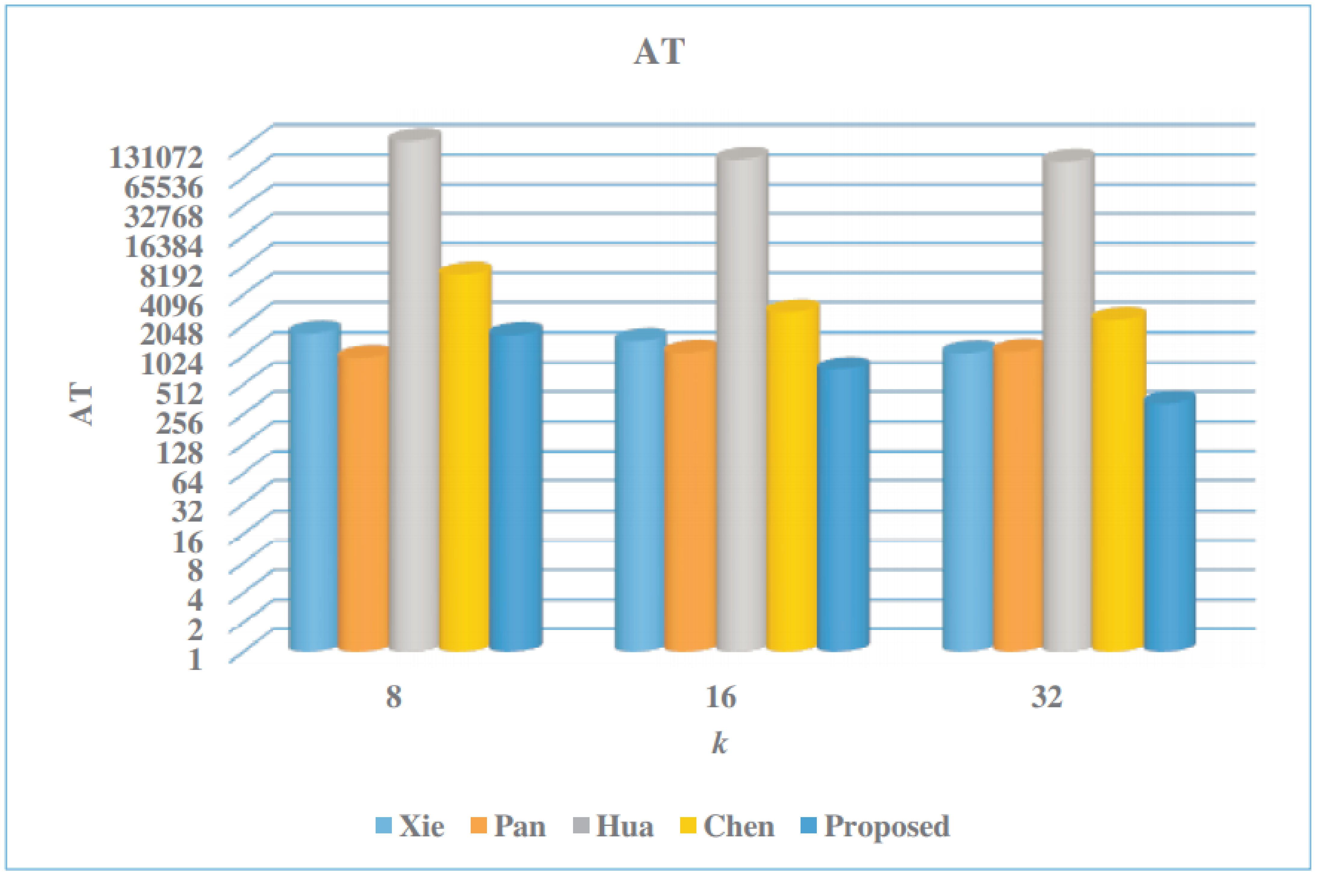
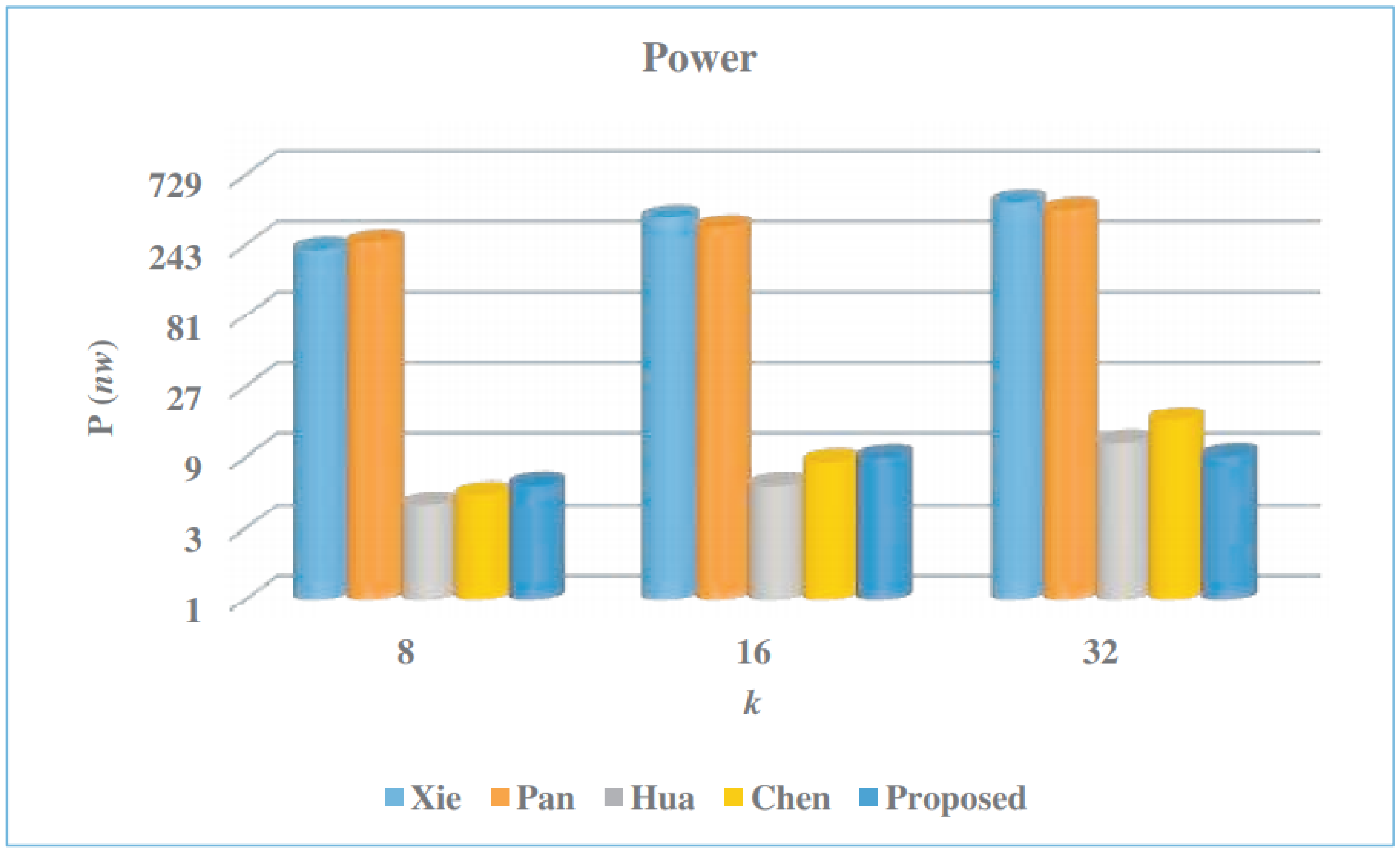
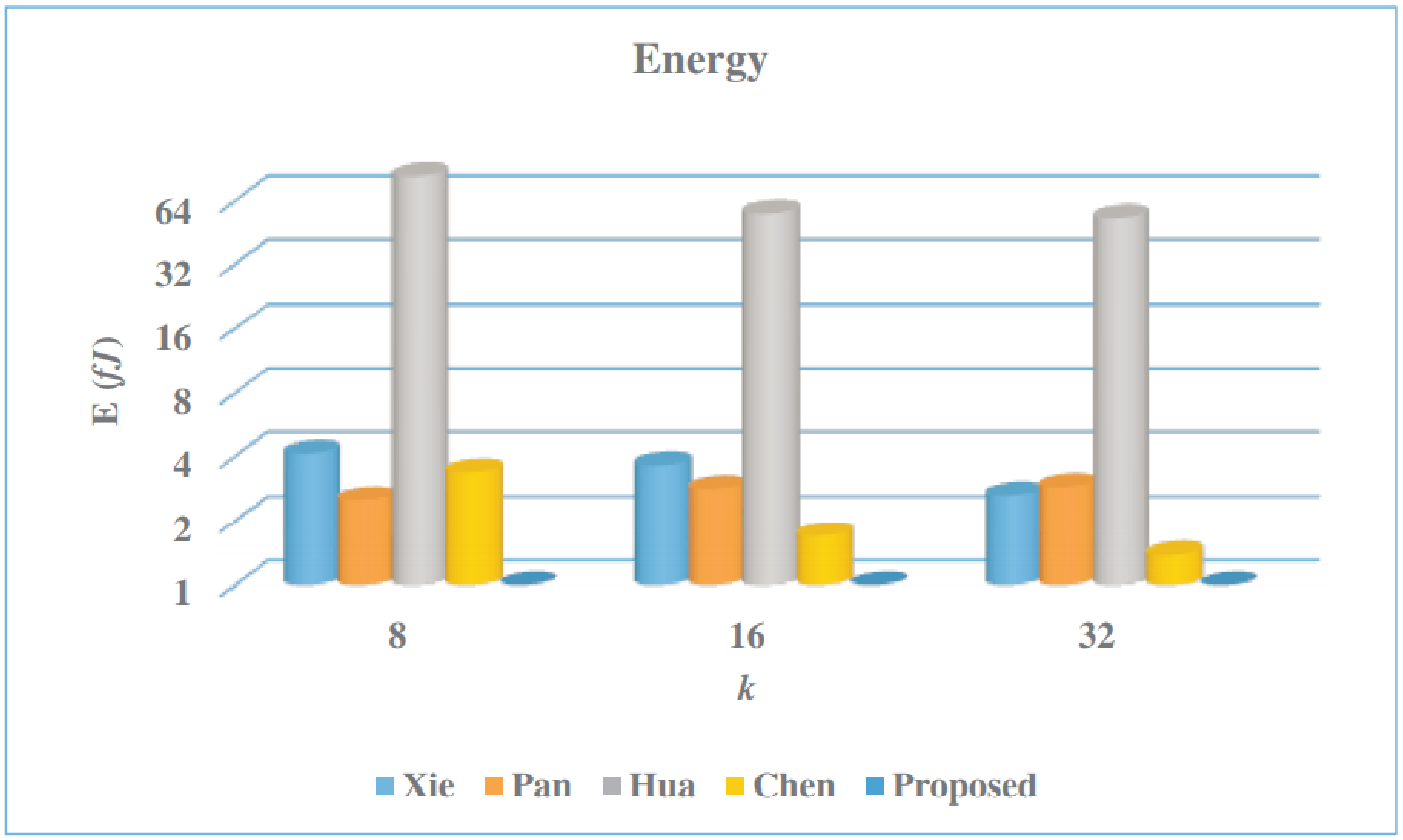
| Multiplier | k | Latency | Area (A) | CPD | Time (T) | AT | Power (P) | Energy (E) |
|---|---|---|---|---|---|---|---|---|
| [Kgates] | [ps] | [ns] | [nW] | [fJ] | ||||
| Xie [50] | 8 | 324 | 92.98 | 56.4 | 18.27 | 1699.0 | 225.56 | 4.12 |
| 16 | 172 | 146.96 | 56.4 | 9.70 | 1425.5 | 375.5 | 3.64 | |
| 32 | 98 | 195.13 | 56.4 | 5.53 | 1078.5 | 477.4 | 2.64 | |
| Pan [45] | 8 | 48 | 97.46 | 206.3 | 9.90 | 964.9 | 252.91 | 2.50 |
| 16 | 36 | 123.93 | 244.4 | 8.80 | 1090.6 | 320.07 | 2.82 | |
| 32 | 24 | 164.34 | 282.5 | 6.78 | 1114.2 | 425.09 | 2.88 | |
| Hua [60] | 8 | 259,584 | 7.99 | 73.4 | 19,053.47 | 152,237.2 | 4.35 | 82.88 |
| 16 | 129,792 | 10.40 | 73.4 | 9526.73 | 99,077.9 | 5.85 | 55.73 | |
| 32 | 64,896 | 19.91 | 73.4 | 4763.37 | 94,838.7 | 11.15 | 53.11 | |
| Chen [61] | 8 | 11,946 | 10.16 | 55.2 | 659.42 | 6699.7 | 5.11 | 3.37 |
| 16 | 4678 | 13.51 | 55.2 | 203.03 | 2742.9 | 8.38 | 1.70 | |
| 32 | 1572 | 26.58 | 55.2 | 86.77 | 2306.4 | 15.95 | 1.38 | |
| Proposed | 8 | 1325 | 12.87 | 96.0 | 127.2 | 1637.1 | 5.91 | 0.75 |
| 16 | 364 | 13.98 | 145.0 | 52.8 | 737.9 | 8.95 | 0.47 | |
| 32 | 104 | 15.34 | 207.0 | 21.5 | 330.2 | 9.14 | 0.19 |
Publisher’s Note: MDPI stays neutral with regard to jurisdictional claims in published maps and institutional affiliations. |
© 2021 by the authors. Licensee MDPI, Basel, Switzerland. This article is an open access article distributed under the terms and conditions of the Creative Commons Attribution (CC BY) license (https://creativecommons.org/licenses/by/4.0/).
Share and Cite
Ibrahim, A.; Gebali, F. Energy-Efficient Word-Serial Processor for Field Multiplication and Squaring Suitable for Lightweight Authentication Schemes in RFID-Based IoT Applications. Appl. Sci. 2021, 11, 6938. https://doi.org/10.3390/app11156938
Ibrahim A, Gebali F. Energy-Efficient Word-Serial Processor for Field Multiplication and Squaring Suitable for Lightweight Authentication Schemes in RFID-Based IoT Applications. Applied Sciences. 2021; 11(15):6938. https://doi.org/10.3390/app11156938
Chicago/Turabian StyleIbrahim, Atef, and Fayez Gebali. 2021. "Energy-Efficient Word-Serial Processor for Field Multiplication and Squaring Suitable for Lightweight Authentication Schemes in RFID-Based IoT Applications" Applied Sciences 11, no. 15: 6938. https://doi.org/10.3390/app11156938
APA StyleIbrahim, A., & Gebali, F. (2021). Energy-Efficient Word-Serial Processor for Field Multiplication and Squaring Suitable for Lightweight Authentication Schemes in RFID-Based IoT Applications. Applied Sciences, 11(15), 6938. https://doi.org/10.3390/app11156938