Review

Active and Quantum Integrated Photonic Elements by Ion Exchange in Glass

by
Giancarlo C. Righini
1,† and
Jesús Liñares
2,*,†
1
Microdevices for Photonics Laboratory (MIPLAB), Nello Carrara Institute of Applied Physics (IFAC-CNR), Via Madonna del Piano 10, 50019 Metropolitan City of Florence, Italy
2
Quantum Materials and Photonics Research Group, Optics Area, Department of Applied Physics, Faculty of Physics/Faculty of Optics and Optometry, Universidade de Santiago de Compostela, Campus Vida s/n, E-15782 Santiago de Compostela, Galicia, Spain
*
Author to whom correspondence should be addressed.
These authors contributed equally to this work.
Appl. Sci. 2021, 11(11), 5222; https://doi.org/10.3390/app11115222
Submission received: 19 April 2021 / Revised: 27 May 2021 / Accepted: 28 May 2021 / Published: 4 June 2021
(This article belongs to the Special Issue Ion-exchange in Glasses and Crystals: from Theory to Applications )

Abstract

:
Ion exchange in glass has a long history as a simple and effective technology to produce gradient-index structures and has been largely exploited in industry and in research laboratories. In particular, ion-exchanged waveguide technology has served as an excellent platform for theoretical and experimental studies on integrated optical circuits, with successful applications in optical communications, optical processing and optical sensing. It should not be forgotten that the ion-exchange process can be exploited in crystalline materials, too, and several crucial devices, such as optical modulators and frequency doublers, have been fabricated by ion exchange in lithium niobate. Here, however, we are concerned only with glass material, and a brief review is presented of the main aspects of optical waveguides and passive and active integrated optical elements, as directional couplers, waveguide gratings, integrated optical amplifiers and lasers, all fabricated by ion exchange in glass. Then, some promising research activities on ion-exchanged glass integrated photonic devices, and in particular quantum devices (quantum circuits), are analyzed. An emerging type of passive and/or reconfigurable devices for quantum cryptography or even for specific quantum processing tasks are presently gaining an increasing interest in integrated photonics; accordingly, we propose their implementation by using ion-exchanged glass waveguides, also foreseeing their integration with ion-exchanged glass lasers.

1. Introduction

Ion exchange in glass has been exploited since the early Middle Ages to color (stain) glasses: marvelous stained glass windows, obtained by ion exchange from a silver paste, are still visible in many European cathedrals. The technique of staining glass yellow by painting it with silver salts was already in use in the 14th century: the glass painter Antonio da Pisa, besides creating, in 1395, a superb window in the south door of Florence Cathedral (Figure 1), was the author of a treatise on glass painting, where he shortly described how to produce the yellow color [1]. The glass surface is coated with a silver compound dispersed in a clay medium; during the heating just above the glass transition temperature the silver ions are exchanged with the alkali ions present in the glass (mostly Na + or K + ), which then diffuse into it. Subsequently, due to the presence of impurities in the glass, silver ions reduce to metallic silver nanoparticles; the resulting color depends on the size, shape and concentration of the nanoparticles.
For large-scale industrial applications, however, the ion-exchange technology had to wait until the beginning of 20th century, when the chemical surface tempering of glass started to be used [2]. The process (sometimes also called ion stuffing or just chemical strengthening) became a standard in the industry in the 1960s, when, for instance, Corning developed Chemcor® glass, a chemically strengthened glass that was intended to be used in phone booths, prison windows, eyeglasses and automobile windshields. In parallel to these events, there were interesting advances in the optical field, too: in the 1910s it was observed that the ion-exchange process was also inducing a change in the refractive index of the glass, and in the 1960s integrated optics moved its first steps, with waveguiding structures that required materials having slightly different refractive indices [3].
Since then, ion exchange has been proven to provide an excellent technological platform for optical integration. Optical waveguides in glass by ion exchange were first fabricated in 1972 using electrically induced migration of thallium ions into a borosilicate crown glass that contained K 2 0 and Na 2 O [4], but soon waveguides were also produced by thermal ion exchange from thallium, potassium or silver nitrate, with Ag + giving the best results (besides also being much safer than Tl + ) [5]. Quite obviously, there was also a growing industrial interest, as testified by several patents; for instance, the US Patent 3,857,689 by K. Koizumi et al., filed in 1972 and published in 1974, concerned the “Ion exchange process for manufacturing integrated optical circuits” [6]. Figure 2 shows a schematic view of the process, where the glass plate (11) with the Ti mask (12) is immersed in a molten salt bath (13); as an example, the patent indicated that for a Schott F2 lead silicate glass the process produces a surface refractive index difference Δ n = 0.005 when immersing the glass for about 3 h in a molten salt bath heated at 450 ° C and containing Tl 2 SO 4 and ZnSO 4 at an equal mole ratio [6].
Almost at the same time, the US Patent 3,836,348A by T. Sumimoto et al., filed again by Nippon Selfoc Co. Ltd. in 1973 and published in 1974, presented a “Method for manufacturing optical integrated circuits utilizing an external electric field” [7]. They claimed that, by using Tl + ions and an electrical field to drive the ion diffusion, a refractive index profile close to a rectangular one can be achieved.
In the following years, the fabrication technology of glass waveguides employing several ion exchangers (K + , Cs + , Rb + , Cu + , Li + and so on) experienced a great development, and commercial devices were designed and tested (see, for instance, Reference [8]). In parallel, ion-exchange technology was also exploited to create gradient index (GRIN) glass rods [9] and rod lenses with parabolic index profile, suitable for photographic systems [10] and also in conventional optical systems [11] but mostly for laser-to-fiber or fiber-to-fiber coupling [12]. Recently, it was shown that the use of GRIN lens cascades is opening up many surprising applications, spanning from quantum optics to clinical diagnostics [13].
Further theoretical and experimental advances completed the foundations of what is now a fully mature technology for integrated optics and photonics; with time, several very interesting review papers appeared, showing the gradual progresses of this R&D field, up to the use of femtosecond lasers to drive the ion diffusion in glasses [14,15,16,17,18,19,20,21]. Moreover, as ion exchange in glass allows producing either surface or buried waveguides, this technology is promising for 3D integration, too [22,23].
A sketch of the K + /Na + exchange process, which is exploited quite often because it guarantees waveguides with low propagation loss, is shown in Figure 3 [24]. The K + ions from the molten salt enter the glass, whereas Na + ions from the glass move to the melt, in order to keep the electrical neutrality. This type of exchange has two drawbacks: the induced refractive index variation Δ n is lower than 10 2 (so, only a weak guide confinement is possible), and it introduces some birifringence, due to the compressive stress induced by the difference in ionic radius between Na + and K + ions. On the other hand, as already mentioned, this stress may also be exploited to increase the mechanical resistance of the glass itself (chemical strengthening).
The Ag + /Na + ion exchange, instead, thanks to the similar size and the difference of polarizability of the two ions, allows a higher Δ n ( 10 1 ) without birefringence and also the burial of waveguides in a two-step process, as sketched in Figure 4. Unfortunately, silver, too, has some limits: in the presence of humidity, surface waveguides (which are used in sensing devices, interacting with external medium) suffer higher losses, due to chemical reduction to metal silver. An approach useful to overcome this limitation is to use the Tl/Na process [25]: in this case, a drawback is due to the toxicity of thallium. Thus, we must conclude that the choice of the ion pair to be used in the waveguide fabrication by ion exchange is dictated by the characteristic (optical, mechanical, safety) one wants to privilege.
In this paper, the focus is on glass ion-exchanged integrated optical devices: their applications cover broad areas, where optical sensing and optical communications are at the forefront. Thus, in the field of optical sensing, many integrated optical sensors are based on the properties of the evanescent modal optical field, and ion-exchanged waveguides offer the advantage of the proximity between the glass index (n = 1.5) and the index of frequently used organic compounds (around 1.4–1.6) and of aqueous solutions (index close to 1.33). These guided-wave structures lead to large evanescent fields, which maximize the optical sensitivity function. A large amount of optical integrated sensors and biosensors based on ion-exchanged glass waveguides have been proposed [18,19,20,26] and keep being implemented in the last years [27,28,29,30]. An interesting example may be represented by a 32-analyte integrated optical fluorescence-based multi-channel sensor and its integration to an automated biosensing system [31]. Figure 5 shows the layout of the fiber-pigtailed sensing chip consisting of a single-mode channel waveguide circuit that distributes the light to 32 separate sensing patches on the chip surface. The use of this waveguide immunosensor, based on a K + -exchanged BK7 glass, was demonstrated for the detection of Microcystin-LR cyanotoxin in two real lake water samples taken from Fuhai lake and Beihai lake in Beijing [31].
In the field of optical communications, the high optical compatibility between glass integrated devices and optical fibers clearly offers an important advantage with respect to other materials. Again, ion-exchanged glass waveguides have constituted a fundamental component of several devices based on modal coupling, such as directional couplers (e.g., for power dividers), gratings (e.g., for contradirectional coupling in integrated lasers), multimode interferometers (MMI), 1 × N and 2 × N splitters, array waveguide gratings (e.g., for wavelength division multiplexing), and so on [19,32,33]. Section 2 summarizes the fundamentals of ion-exchanged channel waveguides and circuits. By using suitable glass substrates, such as rare-earth doped oxide glasses, active integrated optical devices may also be fabricated through ion exchange; this topic is discussed in more detail in Section 3 of this paper. Other interesting aspects concern the manufacturing of nonlinear optical (NLO) integrated devices: Jackel et al. [34], in 1990, designed two glasses, containing Ti and Nb to increase the nonlinear index coefficient and an alkali ion (Na + or K + ), so to have a large optical nonlinearity and to be compatible with ion exchange. Spatial soliton propagation in these waveguides was demonstrated, which proved the possibility of implementing an all-optical switch. Almost at the same time, tests were also performed on commercial semiconductor-doped glasses, which had been proven to possess nonlinear optical properties [35,36]: optical waveguides were fabricated by using a Cs + - K + exchange [37]. Ion-exchanged waveguides may also be capable of handling high laser powers, e.g., from an integrated Q-switched laser [38], and are therefore suitable, due their intrinsic light confinement properties, for nonlinear applications [39]. In that area, however, hybrid structures may be more efficient and the coupling of a lithium niobate film with a ion-exchanged glass waveguides can lead to the manufacturing of electro-optic modulators or second harmonic generators [40].
Many other applications are possible, also linked to the new topics emerged in the last years, as for example integrated quantum photonics (IQP) for the implementation of tasks in quantum information, particularly, in quantum communications. It has been underlined that in IQP ’the big challenge is how to realize a scalable, convenient platform for practical deployment and commercialization’ [41]. Indeed, the growth of this area requires the design and fabrication of passive and active integrated devices to be used, for example, in quantum photonic simulation, quantum cryptography, quantum photonic sensors and so on. It is well known that, since the early experiments on silica-on-silicon structures [42], different platforms have been proposed for the implementation of IQP, including those ones silicon-based, III-V semiconductors and lithium niobate [43,44,45,46]. It is very difficult, however, for a single material to meet the stringent demands of most quantum applications, so that hybrid platforms combining different technologies in a single functional unit may have greater success [47]. Silica-based platforms have been considered, too, but only with reference to femtosecond laser written circuits [44,48]. To our knowledge, despite the suggestion, several years ago, by the group of one of the present authors [49], a platform based on ion-exchanged glass (IExG) circuits has not been considered so far as an effective integration technology for quantum photonics. This topic is discussed in more detail in Section 4, where we present a brief review of the most incipient proposals and results in the field of quantum circuits based on an IExG platform. Likewise, it is shown that with hybrid glasses active and quantum integrated devices can be combined in an efficient way by using IExG platform, in particular, IQP devices for generating and detecting quantum states are presented; hybrid integration with lithium niobate films may also permit the realization of efficient nonlinear integrated devices [40]. Finally, we present in Section 4 the design, fabrication and preliminary experimental results of a quantum projector for detecting quantum states by projective measurements, for example for quantum cryptography through multicore optical fibers (MCF) [50,51] or even few-mode optical fibers (FMF) [52]; the primary aim is to make clear the potentiality of the IExG platform for integrated quantum photonics.

2. Fundamentals of Ion-Exchanged Glass Waveguide Circuits

There are excellents works on ion-exchanged glass waveguide circuits, but here we focus our attention on circuits formed by elements as channel waveguides, directional couplers and optical gratings (contradirectional couplers), and intended for classical and quantum optical sensing and communications. Channel waveguides are the pillar of integrated optics [17,18,19,53,54] and optical integrated gratings are also fundamental for the implementation of many devices, including integrated amplifiers and lasers in rare-earth doped glasses [19,55]. Directional couplers and 1 × N splitters, too, are based on channel waveguides and have been mainly intended for power derivation in optical fiber communication networks, but they also play an important role in optical sensing and in interferometry [31,56], including applications to optical astronomy [57]. The fabrication of these devices in a glass substrate usually requires a lithographic process [18,19] in order to allow a spatially selective ion-exchange. Let us refer to thermal ion exchange: first, a metallic film (Al or Ti) is deposited on the glass substrate, followed by the deposition of a photoresist film. After UV exposure through a given mask and a subsequent chemical etching, the mask pattern is transferred to the metal film, so that, when immersing the substrate in a molten salt, the ion exchange occurs only in the volume under the designed opening. This process produces surface channel guides, which can be slightly buried by a second thermal diffusion process or strongly buried by using an electrical field.
In Figure 6, the design is shown of an integrated optical device of arbitrary dimension N, that is, N optical paths (channel waveguides) coupled by concatenated directional couplers (DC) and phase shifters (PS). It represents a generic optical device able to implement different passive quantum operations. Active functions, such as optical generation and amplification, may also be added if hybrid glasses, with a portion doped by rare earth elements (on the left in Figure 6), are used.
We must stress that hybrid glasses can be obtained by joining a block of a passive glass with a block of an active glass by a low temperature bonding technique [58,59]; alternatively, the hybrid glass can be also implemented by bonding an active glass superstrate to a passive glass substrate [60]. Consequently, integrated lasers having optical gratings (OG) resonators can also be included in the integrated circuit, as sketched in Figure 6; they are pumped by an external signal P j ( j = 1 , , N ), which can generate classical and/or quantum light states [61]. The optical gratings can be fabricated by laser writing or by the same photolithographic procedure described above [17,18,19]. In short, Figure 6 shows a general ion-exchanged hybrid glass integrated optical circuit highly intended for classical/quantum communications (or even classical/quantum optical sensing) and that can be adapted for implementing different devices as wavelength multiplexers, quantum states generators, quantum states projectors and so on, as is shown in some detail in Section 3 and Section 4.
The total refractive index profile of the above ion-exchanged hybrid glass integrated optical circuit can be represented, in a good approximation, as follows
n ( x , y , z ) = n s + j Δ n j ( x , y , z ; p j 1 , , p j q )
where n s is the substrate index, and Δ n j ( x , y , z ; p j 1 , , p j q ) , j = 1 , , N are functions describing the refractive index profile obtained in each ion-exchanged channel waveguide with parameters p j 1 , , p j q , that is, ion-exchanged parameters as effective depth d, maximum refractive index change Δ n , …, geometrical lithographic parameters as width w of a channel guide, separation s between channel guides, …and so on. The centers of the channel guides (usually the position of the maximum refractive index) follow paths described by functions f j ( z ) , that is, z-functions representing translations of a refractive index profile. A typical case is a channel guide j, which is bent along S-shaped transitions to couple it with other parallel channel guide j + 1 . These transitions may follow, for example, the path described by Minford et al. (Minford curve) for obtaining low losses [62]. An example of a refractive index profile representation for an arbitrary channel guide j is the following (from here and for the sake of simplicity we omit subscript j)
Δ n ( x , y , z ) = Δ n Erfc x d o x exp { ( y f ( z ) ) 2 d o y 2 }
where Erfc is the complementary error function, which is a typical solution for linear ion exchange, although more general solutions can be chosen [17,63,64,65], f ( z ) is the curve (path) profile, Δ n is the maximum refractive index change and d o x and d o y are effective depths along x and y direction. Note that we have assumed a factorizable index profile, Δ n ( x , y , z ) = Δ n E ( x ) G ( y , z ) , that is, a product between an index profile in depth (x-direction) and a Gaussian index profile along y and z directions describing quite well the lateral diffusion. In many cases such a factorization is a good approximation, or even it can be forced for the sake of design simplicity [66]. Moreover, it is well known that there are different approximate methods to be used in order to obtain manageable mode solutions such as, for example, the effective index method (EIM) [16,66], perturbative and variational methods [16] and so on. On the other hand, this kind of function can also describe the change of index or geometry for other integrated optical elements as phase shifters, for example, those based on an adiabatic approximation that could be represented by the following function
Δ n ( x , y , z ) = Δ n Erfc ( x / d o x ) exp { y 2 d y 2 ( z ) }
Note that in this case we have a rectilinear channel waveguide ( f ( z ) = 0 ) with d y ( z ) an adiabatic z-function and therefore the effective index changes slowly on z and thus a well defined phase shifting can be obtained.
We must recall that the cornerstone of the ion-exchange method is that these functions are, in a good approximation, proportional to the concentration C j ( x , y , z ) of exchanged ions. In fact, the q parameters p 1 , , p q such as maximum refractive index change Δ n , effective depth d o x , lateral effective depth d o y and so on, can be expressed in an empiric way as functions of both the fabrication physical parameters, such as temperature T, ionic concentration [ C ] of the molten salt (or ionic concentrations [ C 1 , C 2 , ] , as in the case of molten salts eutectic mixtures), ion-exchange time t and also geometrical parameters, as width of the channel guide mask w, separation between channel guides s and so on. We must also underline that, although an empiric approach can be sufficient in many cases to determine the fabrication parameters, a great amount of research work has been devoted to a rigorous physical modeling and numerical simulation of ion exchange in glass, which in turn, is related to the development of different theories on ion exchange in glass [15,67,68,69,70,71]. These physical/numerical approaches can be required when the refractive index profile must be known with a great accuracy. In any case, one of the main aims in integrated optical circuits is to obtain single-mode channel guides (paths) that are coupled in certain regions by directional coupling and with phase shifters suitably located, as shown in Figure 6 to achieve an integrated optical circuit with a specific purpose. Finally, it is also worth indicating that sometimes two-mode or even few-mode waveguides can be considered. The modes can be considered in plane yz or also in depth x. In the latter case, it can be considered as a type of three-dimensional integration [27,72]. On the other hand, two-mode guides in the yz plane have also been considered, for example, for spatial multiplexing [73].

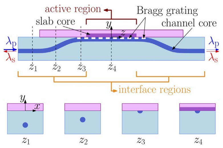
3. Ion-Exchanged Active Integrated Photonic Devices

As already briefly mentioned in the previous sections, ion exchange may occur in a variety of substrates and using many different ions. The process, however, can be easily performed especially when using univalent ions and glasses whose composition includes alkali ions as glass modifiers. Similarly, in crystalline materials such as lithium niobate, only Li + ions are effective and they exchange with H + ions. These limitations, however, are not very critical, as testified by the large number of photonic devices that have been successfully implemented. Among those devices, a very important class is constituted by the active ones, i.e., integrated optical frequency converters, amplifiers and lasers. Let us here briefly overview some of the excellent results already achieved, limiting ourselves to devices produced by ion exchange in rare-earth-doped (RED) glasses.
It has already been mentioned that RED glasses constitute an excellent physical medium for generating and amplifying light. Indeed, oxide glasses are well-known as excellent hosts for rare-earth ions: not by chance, one of the very first solid-state lasers was demonstrated in 1961 by Snitzer in American Optical Company using a Nd 3 + -doped glass [74]. In that same year Snitzer and colleagues constructed and operated the world’s first optical fiber laser and three years later the first optical fiber amplifier [75]. Even the first thin-film waveguide glass amplifier, in 1972 [76], and the first integrated optical glass laser, in 1974 [77] were implemented in the same material, Nd 3 + -doped glass and operated at ~1.06 μm wavelength. It has to be noted that, whereas the amplifier was fabricated by RF-sputtering deposition of the doped guiding film, the waveguide laser was indeed realized in a Nd-doped borosilicate glass by using the double-diffusion process with an electric field already reported by Izawa and Nagakome [4]. The channel waveguides had an almost circular profile, and the pump threshold was around 18 μJ, namely about one half of the threshold of the corresponding bulk laser [77].
The excellent properties of ion-exchanged waveguide lasers had therefore been demonstrated, but a strong interest in these devices emerged only much later, after the implementation, around 1985, of the second generation of fiber communication systems, which used single-mode fibers. Thus, for instance, in 1989 Najafi et al. studied the fabrication of optical waveguides in commercial Kigre Nd-doped lithium-silicate glass by means of Ag-Li exchange and verified that the process did not influence the emission properties of Nd [78]. In 1990, a waveguide laser emitting at 1054 nm was reported by Aoki et al. [79]; the laser, end-fire pumped by a diode-laser operating at 802 nm, was capable of a maximum output power higher than 150 mW. It was fabricated in a Nd 3 + -doped glass (Hoya LHG-5 phosphate glass, 3.3 wt% Nd) by using field-enhanced silver ion exchange. The same group also demonstrated a gain of 3.4 dB at 1.054 μm and an efficiency of 0.027 dB/mW in a 10 mm long waveguide amplifier pumped with an argon-ion laser [80]. Several other works were performed in the early 1990s concerning Nd-doped waveguide lasers and amplifiers, still using ion-exchange fabrication technology [81,82,83,84,85]; it was also proven that distributed Bragg reflector (DBR) integrated lasers could be fabricated by realizing holographically an OG in photoresist and then etching it into the channel guide by argon ion milling [83]. By using ion exchange in a semiconductor microcrystallite-doped glass second harmonic generation of Nd:YAG laser radiation was also achieved [36].
In the meantime, the evolution of fiber communication systems continued and saw the introduction of 1.5 μm laser diode sources, owing to the fact that silica fibers have the lowest propagation losses in that wavelength window. Fiber lasers and amplifiers had therefore to use another rare earth than Nd, with photoluminescence emission in the near infrared band: this was Erbium, which is characterized by a strong emission at 1.532 μm. Er-doped fiber amplifiers (EDFAs) soon became a very important component of fiber transmission systems, that needed regeneration and re-amplification of the guided light after a certain distance, of the order of tens of kilometers. Most of the pioneering research on EDFAs was performed at Southampton University by the David Payne’s group and at AT&T Bell Labs by Emmanuel Desurvire and colleagues: the two groups published the first successful results almost at the same time, in 1987 [86,87]. A strong limitation to the practical use of these early fiber amplifiers was related to the pump signal: Payne’s group was using pump wavelengths in the range 655–675 nm, whereas Desurvire used a pump at 514.5 nm. In both cases, bulk pump lasers were necessary. A substantial step forward market diffusion of EDFAs was made with the availability of powerful laser diodes. Then, the demand of ever increasing system transmission capacity and of a mechanism for creating multipoint networks led to the use of the wavelength division multiplexing (WDM) technology. As integrated optical devices could offer a cheap and small-footprint approach to the fabrication of WDM devices, a renewed R&D interest was focused on Er-doped glass devices and to the integration of passive and active functions on a same glass substrate. An issue, however, was related to material requirements, much more stringent for integrated optics than for fibers, due to the different fabrication technologies and to the much higher rare-earth concentration required in short-length planar devices. An interesting effort to assess the relative merits of different compositions of the host glass was published by Miniscalco in 1991 [88]. He concluded that ’in most situations’ Al-doped silica was the preferred glass for Er 3 + -doped fiber amplifiers at 1500 nm. In planar short-length devices, silicate glasses may suffer even more from the lower solubility of rare-earth-ions with respect to phosphate glasses, since it may lead to clustering and reducing the conversion efficiency. In spite of this, the first ion-exchanged waveguide laser emitting at 1540 nm used a silicate BK7 glass containing 0.5 wt% Er 2 O 3 [89]. The laser cavity was formed by bonding dielectric mirrors to the chip end facets, and a thermal ion exchange in a KNO 3 bath was employed in waveguide fabrication. In the same year 1992, an Er-doped waveguide amplifier with 0.65 dB/cm net gain with 100 mW pump power was demonstrated [90]. This device was constituted by a phosphorus-doped silica core doped with 0.55% wt Er and silica cladding, deposited by flame hydrolysis on a silicon substrate. Quite obviously, owing to the appeal of erbium-doped waveguide amplifiers (EDWAs), various technological approaches to waveguide fabrication were pursued, with deposition techniques of doped glass films (e.g., RF-sputtering, sol–gel, PECVD, flame hydrolysis) competing with diffusion techniques (ion exchange, ion implantation) in bulk doped glasses [20]. As an example of RF-sputtered amplifying waveguides, a net optical gain of 4.1 dB/cm at 1.535 μm was achieved by Polman et al. by depositing Er-doped multicomponent phosphate glass films [91]; the same group also reported about the possibility of using MeV ion implantation to introduce erbium in a variety of thin films, from oxide glasses to ceramics and to amorphous and crystalline silicon [92].
A commercial interest was also emerging. Among the glass suppliers, the Corning company was particularly interested in the development of ion-exchangeable Er-doped glasses and of amplifiers, as testified also by two patents [93,94]; in the latter one, an optimized composition of a boron-free silicate glass that could be doped with up to 5% wt erbium oxide and ion exchanged with thallium is described [94]. More waveguides and devices based on Er-doped glass substrates and ion-exchange technology were reported in the following years [90,95,96,97,98,99,100,101,102,103,104,105,106,107]; besides waveguide lasers and amplifiers, optical upconversion devices were investigated, too [101]. At a certain point, phosphate glasses seemed to allow higher performances to ion-exchanged EDWAs, as they could be doped with larger amounts of rare-earth ions than silicates. Even in phosphate glasses, however, high erbium concentrations may produce quenching of the luminescence; moreover, the absorption cross section of Er + ions at ~980 nm is small. Thus, the solution was to add another rare-earth ion as a sensitizer for erbium. Glass co-doping with ytterbium ions has proven to be a very efficient solution: it allows the transfer of energy from excited Yb 3 + ions to close Er 3 + ions through a cooperative cross-relaxation process, with the result of significantly enhancing system absorption at 980 nm and making the pumping mechanism more efficient. Moreover, in the case of high concentration, the Er 3 + ions are closer together, so that deleterious non-radiative energy exchanges between neighboring ions can take place; the presence of Yb 3 + ions is also effective in reducing such unwanted Er 3 + - Er 3 + ion energy transfer interactions by increasing the mean inter-atomic distance. A useful spectroscopic investigation of an extensive series of Er 3 + -doped and Er 3 + -Yb 3 + -co-doped soda–lime–silicate (SL) and aluminosilicate (AS) glasses was also presented in a paper by Hehlen et al. [108]. AS glasses showed higher oscillator strengths and larger inhomogeneous broadening of 4f transitions than SL glasses; it was also suggested that a minimum molar concentration ratio 2:1 of Yb oxide to Er oxide is required to achieve efficient sensitization of Er 3 + . In 1995, an integrated laser was produced by K + /Na + ion exchange in an alkali-rich barium silicate glass containing 17% wt Y 2 O 3 and 1.5% wt Er 2 O 3 [109]. Later, commercial Er-Yb co-doped phosphate glasses became available, too, where single-mode channel waveguides could be produced by K + /Na + ion exchange; a net gain of 7.3 dB in a 6 mm long waveguide amplifier was claimed [110].
EDWA devices with excellent characteristics were obtained in both silicate and phosphate glasses co-doped with Er and Yb; as an example, a lossless 1 × 2 splitter was demonstrated in a buried thallium-exchanged waveguide in a borosilicate glass co-doped with 5% wt Yb 2 O 3 and 3% wt Er 2 O 3 [111]. They measured 2.3 dB/cm gain and 0.07 dB/mW gain efficiency in a 3.9 cm long straight waveguide amplifier with a pump of 130 mW. Almost at the same time, Barbier et al. achieved a 7 dB net gain in a 41 mm long amplifier with double-pass configuration (≈1.7 dB/cm) using a buried waveguide produced by two-step ion exchange in a phosphate glass doped with 2.5% by weight of erbium and 3% by weight of ytterbium [112]. Shortly thereafter, however, the same group reported several impressive advances in EDWA’s implementation, including: an amplifying four-wavelength combiner, consisting of an all-connectorized 4 × 1 glass splitter followed by a 4.5-cm-long Er/Yb-doped waveguide amplifier (≈2.6 dB/cm) [98]; a planar amplifier capable of 3.1 dB/cm net gain [113]; a multiplexer/amplifier gain-block constituted by an amplifying section realized in phosphate glass as a 5.5 cm straight waveguide planar waveguide amplifier and a 980/1550 nm multiplexer realized as a 3 cm long directional coupler in a silicate glass [114]. The amplifier and the multiplexer were assembled together via active alignment followed by bonding with UV curing glue; the module had a fiber-to-fiber gain of 15.7 dB and a noise figure of 4.7 dB at 1535 nm. In all these cases, the amplifier was realized in a phosphate glass co-doped with 2 wt.% erbium and 4 wt.% ytterbium.
In the 2000s, the literature was enriched by several publications in this area, which can be classified into three groups:
(a)
Papers dealing with the synthesis and characterization of rare-earth doped glasses suitable for ion-exchange fabrication of active devices [17,115,116,117,118,119,120,121,122,123,124,125,126,127,128,129,130,131,132,133,134,135,136,137,138,139,140,141,142,143,144].
(b)
Demonstration and characterization of rare-earth doped ion-exchanged waveguide amplifiers and frequency converters [140,145,146,147,148,149,150,151,152,153,154,155,156,157,158,159,160,161,162,163,164,165].
(c)
Demonstration and characterization of rare-earth doped ion-exchanged waveguide lasers [60,61,147,166,167,168,169].
An example of a laser device is shown in Figure 7: it is a 3D hybrid structure, with a channel core waveguide and a slab core waveguide which, in a certain volume, interact with each other and with the Bragg grating that provides the optical feedback necessary for laser action. Figure 8 shows the longitudinal and cross sections of the device. The passive glass is a GO14 silicate by Teem Photonics, whereas the active glass is a IOG-1 phosphate by Schott, doped with 2.2 wt% Er 2 O 3 and 3.6 wt% Yb 2 O 3 . In both glasses, the waveguides are produced by Ag + -Na + ion exchange.
An example of a packaged Er-Yb doped waveguide amplifier (EYDWA) is shown in Figure 9 [155]. The substrates were commercially available Schott IOG-1 phosphate glasses co-doped with 2 wt% Er 2 O 3 and 5 wt% Yb 2 O 3 . Channel waveguides were fabricated by ion exchange using an Al thin film mask and were buried by using a two-step process, namely, a K + -Na + thermal exchange (T = 385 ° C, t = 60 min), followed by a field-assisted annealing (T = 380 ° C, t = 30 min, electric field 120 V/mm) [123]. The figure shows a photo of an EYDWA device packaged by using fiber silicon V-groove arrays and a UV curing glue. In a pigtailed 4.0 cm long EYDWA, a net gain of 8.0 dB and an average noise figure of 5.1 dB were obtained in the 1530–1560 nm band.
New research topics have appeared in those years; some attention, for instance, was focused on the possibility of using ion-exchange technology in rare-earth doped tellurite glasses [121,131,132,133,136,170,171,172]. Tellurite glasses, i.e., glasses based on tellurium oxide, doped with rare earth have been long studied since they have the lowest phonon energy (about 780 cm 1 ) among oxide glass formers and, as a consequence, their radiative quantum efficiency is high. Furthermore, they offer good stability, chemical durability, high solubility of rare-earth ions and exhibit high refractive index and a wide transmission range (0.35–6 μm); these properties make them an excellent host material for amplifiers and lasers to be used in a wider wavelength range, e.g., in S + C + L (1460–1615 nm) or C + L + U (1530–1675 nm) bands of the optical communication systems. As already mentioned, other fabrication technologies were also developed, and sol–gel, for instance, has been a very convenient platform for the fabrication of high quality thin glass films, optical planar waveguides and photonic bandgap structures [173,174,175,176]. An interesting research concerned the possibility of integrating the sol–gel and ion-exchange techniques for the fabrication of passive and active channel waveguides in rare-earth doped integrated optic devices [115,177].
Among the various research lines aiming at improving the characteristics of waveguide optical amplifiers, it is worth mentioning the article by Donzella et al. [160], where another 3D hybrid structure is designed with the goal of making possible the use of a low-cost high-power broad area laser diode, instead of an expensive single-mode 980 nm laser, for the amplifier’s pumping. Their design, sketched in Figure 10 includes direct butt-coupling of the pump light into a multimode passive waveguide (in silicate glass): an Er-Yb doped single mode waveguide (in phosphate glass) is placed on top of the passive one, and light is progressively coupled from bottom to top waveguide, being captured by Yb ions acting as sensitizers for Er ions. Experimental tests with ion-exchanged waveguides fabricated in the two glasses allowed to measure amplified spontaneous emission (ASE); Figure 11 shows the upconversion green light in the upper single mode waveguide, a proof of the effectiveness of the pumping scheme. According to their numerical simulation, gain values of over 3 dB/cm should be achievable.
As already mentioned in Section 2, too, another way of fabricating hybrid active/passive glass structures is to butt join two glass pieces, an undoped one and a rare-earth-doped one, in order to optimize the optical characteristics and minimizing losses. Such a structure was used especially to fabricate lossless splitters and combiners, widely used in telecom systems; to mention some examples, Jaouen et al. separately designed and optimized a passive section in silicate glass and an active section in phosphate glass before joining them by using a UV curing glue, so to produce a lossless 1x8 splitter/combiner [178]. Conzone et al. showed that it was possible to join two aluminophosphate glasses (undoped and doped, respectively) by sandwiching an aqueous phosphate solution between the polished and accurately cleaned surfaces of the two blocks. A rigid joint is formed in 24 h at room temperature. A thermal treatment for 5 h at 375 ° C provides a greater chemical and mechanical robustness [58]. Further, Chen et al. reported a low-cost technique for industrial mass production, which was based on vacuum hot press assisted direct bonding applied to custom made multicomponent silicate glasses [179]. A thermal treatment at 605 ± 20 ° C for 240 min under a pressure of 28 kPa was sufficient to achieve a very good bonding. Figure 12 shows the first bonded sample. The two glasses were germanoborosilicates with sodium oxide for the ion-exchange process; the doped glass contained 0.5 mol% Er 2 O 3 and 1.3 mol% Yb 2 O 3 .
A broad review on Er-Yb laser and amplifiers, covering both the photoluminescence issues and the various materials and technologies, was published in 2011 by Bradley and Pollnau [180]. In the last years, owing to the fact that Er-Yb co-doped ion-exchanged waveguides and devices in silicate and phosphate glasses constitute a mature technology, only very few papers have been published, including some ones related to up–down frequency conversion with application to lighting and solar cells [164,181,182,183,184]. The main research focus has been shifted toward technological platforms that could allow integration with silicon and compatibility with CMOS technology; thus, rare-earth doped aluminum oxide has emerged as a new excellent material. Al 2 O 3 can be deposited by atomic layer deposition or reactive magnetron sputtering, is transparent from the UV to mid IR and exhibits very low propagation losses; the high solubility for rare-earth ions allows it to provide active functions, amplification and lasing, to silicon and silicon nitride platforms. High-gain erbium amplifiers and erbium, thulium and holmium integrated lasers (with emission around 1.5 μm, 1.8 μm and beyond 2.0 μm, respectively) have been demonstrated [185,186,187].

4. Quantum Integrated Photonic Devices

As indicated in the Introduction section, different platforms have been proposed for implementing IQP devices. The main platforms are based on III-IV semiconductor, such as gallium arsenide and indium phosphide, lithium niobate and those ones based on silica such as silica-on-silicon, silicon-on-insulator and silicon nitride, as reviewed, for instance, in References [44,45,46]. IExG platform is not usually included as a possible quantum integrated photonics platform, despite the fact that it is present in many classical optical communications systems and optical sensors. We must indicate that the closest platform to the IExG one is obviously, silica-on-silicon; however, in our opinion, IExG presents a lower technological complexity and retains all the classical advantages of this platform, that is, low-cost, low propagation losses and high compatibility with optical fibers, together with a slightly better modal transverse coupling due to the graded-index profile unlike the strictly step profile of silica-on-silicon waveguides. We must stress that the main limitation, shared with silica-on-silicon, is the low contrast index (therefore low curvature radii and consequently limited device densities). The main consequence is that IExG platform becomes remarkably efficient when quantum applications require only a few qubits. This requirement is fulfilled in most devices for optical quantum communications, optical quantum sensors and even optical quantum simulators. On the other hand, IExG is a passive platform, that is, it has not electro-optical properties and presents a low nonlinearity, although efforts based on glass poling [188] and/or hybrid integration [189] have been made to achieve significant nonlinear effects. Therefore, in a monolithic version, IExG platform would perform only passive functions, but, as shown in Section 3, doping with rare-earth ions adds active functionality [60] and opens new possibilities for integrated quantum photonics. We must also underline that thermo-optic reconfiguration would also be possible in suitable glasses, so providing an additional capability. Accordingly, while applications to quantum computing, as for example the implementation of complex quantum processors for specific or universal purpose, are reserved for other platforms (as lithium niobate, silicon-on-insulator, …), applications requiring a less amount of qubits, as quantum cryptography, quantum optical sensing and even quantum optical simulating, could be implemented by using the IExG platform. A few examples have already appeared in the scientific literature, and the primary aim of this section is to justify such possible applications.
Indeed, recently, theoretical and experimental studies of the IExG platform for implementing different integrated quantum devices has begun to be reported. Thus, numerical modeling of ion exchange in glass for quantum computations tasks has been discussed [190,191]; nanoemitters (nanodiamond) coupled to ion-exchanged glass waveguides for quantum photonics have been realized [192,193]; ion-exchanged glass directional couplers for implementing quantum projectors have been proposed [194]. On the other hand, ion-exchanged waveguides in thin glass substrates, suitable for photonic system integration and EOCB (electro-optical circuit board) panel size integration [195], can open new possibilities in IQP. Likewise, other proposed quantum systems could be implemented, as, for example, quantum simulators of geometrical phases [72] and boson sampling [196], quantum random walk devices [197] and so on. As commented, these implementations will be efficient as long as a few qubits are considered, a limit which is in turn related to the present scalability difficulty of quantum integrated photonics. Thus, ion-exchanged glass devices can provide optimal solutions in quantum optical communications, in particular integrated quantum devices for quantum cryptography [49,51,198] as for example generators of quantum states, quantum projectors and Bell states measurement devices. Likewise, experimental results of these devices fabricated by ion exchange in glass provide proofs of concept about the use of ion-exchanged glass integrated optics in quantum information; but as it will be shown these devices would use well-known ion-exchanged glass integrated optical elements as directional couplers (see, for instance, References [199,200,201]), integrated optical gratings (see, for instance, references [17,18,19]) and so on. Therefore, we have many of the basic ingredients to develop IQP in a IExG platform and we only need to design such quantum devices (quantum circuits), fabricate them and optimize their performance. For example, preliminary results of a quantum projector fabricated by Na + /K + ion exchange in soda-lime glass has been recently proposed [194].
In all cases, the quantum circuits consist mainly of N channel waveguides or paths (N-dimensional device) formed by a set of concatenated integrated optical elements as directional couplers and phase shifters [49] performing quantum operations. As mentioned passive integrated optical elements allow the implementation of devices to be mainly used in quantum communications through different kinds of optical fibers as multicore optical fibers [50] and few-mode optical fibers [52]. On the other hand, it may be useful to recall that space multiplexing is one of the most promising method for increasing the transmission capacity of optical fiber systems [202,203] and that spatial multiplexing can be used for implementing high-dimensional quantum cryptography. At this regard, ion-exchanged glass modal converters have been already successfully used for spatial multiplexing in few-mode optical fibers [52,204,205,206,207,208,209]. These components are located at the emitter and receiver, where one can already place the ion-exchanged glass IQP devices to generate or measure quantum light states excited in the optical modes of a few-mode optical fiber.
Regarding the manufacturing of these devices, we must stress, as commented, that generation and measurement of quantum states in quantum communications can be made with devices formed by the same integrated optical elements fabricated on IExG platform and used in classical optical communications (directional couplers, 1 × N splitters, optical gratings and so on). Therefore, from an industrial point of view, the existing manufacturers of photonic devices on IExG platform can easily enlarge their production to devices designed for quantum optical communications, or even other applications as optical quantum sensors and optical quantum simulators. These applications are well considered by many companies, and governments all over the world invest in quantum technologies that have a disruptive potential. For example, the European Commission has launched in 2018 an ambitious flagship initiative for quantum technologies [210] where, for example, quantum communications play a central role [211,212] for both increasing commercialization of research results and the interest of large industrial players. On the market side, a recent report by Allied Market Research estimated that the market size of integrated quantum optical circuits could grow from a value of 426.0 million USD in 2017 up to 1460.2 million USD by 2025 [213].
In order to make clear the above considerations, and after describing, for the sake of completeness, the fundamental aspects of quantum integrated optical elements in Section 4.1, we present, in Section 4.2, an integrated generator of quantum light states | L based on the use of integrated optical lasers and directional couplers and mainly intended for quantum cryptography. Such a quantum states generator device is designed for the BB84 quantum key distribution scheme [214] and with two-dimensional quantum states, although it can be extended to N-dimensional quantum states [51]. In this device, we propose to use a rare-earth-doped glass, as discussed in Section 3, for generating four weak laser signals obtained by pumping beams, that is, to use a hybrid glass. On the other hand, the passive part of the above device can in turn be used as an integrated quantum projector, of a high interest in quantum devices, particularly and once again, in quantum cryptography [215,216]. Moreover, another device for measuring Bell states is also described, which is of a great importance in MDI (measurement device independent) protocol [217], which is based on the use of two-photon states unlike the BB84 protocol that uses a single photon. Experimental results on a single photon two-dimensional quantum projector is presented in Section 4.3.

4.1. Fundamental Aspects of Quantum Integrated Optical Components

The use of quantum light states in integrated optical devices allows to develop different on-chip applications in quantum optical communications and in other fields such as quantum photonic simulations [196] and quantum photonic sensing [218]. Rigorous theories of linear and nonlinear quantum spatial propagation states in integrated waveguides can be used [219,220,221,222], which allows us to study and design linear and nonlinear quantum integrated optical elements. Moreover, we consider three types of quantum states of a great interest for proofs of concept as the coherent states, the single photon states and the biphoton states. Single photon states, and in particular 1-qubits and 1-ququart states (dimension d = 4 ), have a high interest, for instance, in quantum cryptography; 1-ququart are the states giving rise to the beginning of the so called high dimension quantum cryptography with 1-qudits ( d = N > 2 ), that is,
| L s   = j = 1 N c j | 0 1 j 0 j = 1 N c j | 1 j
where subscript s stands for single-mode photon. This single photon state | L s shows that the photon is in a quantum superposition in the N channel waveguides. Moreover, by using 1-qudits states we can form quantum bases of orthogonal states. These bases have to be in turn mutually unbiased bases (MUBs), which requires | c 1 |   = =   | c N | [198]. On the other hand, lasers emit coherent states | α , with α C , then by using, for instance, a 1xN splitter or a cascade of directional couplers [51] a multimode coherent state | α 1 α N is obtained. It is well known, however, that for weak coherent (wc) states regime, | α i |   1 , an approximated multimode single photon state is achieved, that is, | L w c   | 0 0   + j = 1 N α j | 0 1 j 0 . These states are less efficient because there is a single photon state with a small probability, but it is enough for quantum cryptography.
Next, it is worth describing the quantum mechanical treatment of the basic passive integrated optical elements of our integrated circuits, that is, the directional couplers 2 × 2 and phase shifters. We must stress that these 2 × 2 integrated optical elements (couplers and phase shifters) are enough to generate unitary transformations of dimension N, that is, SU(N) transformations, by concatening properly such optical elements [216]. Let us start by considering a two-dimensional quantum problem ( N = 2 ), that is, the single photon quantum states are 1-qubits, namely, | L s   = c o 1 | 1 1   +   c o 2 | 1 2 , with 1 and 2 denoting two single mode channel waveguides. Synchronous directional couplers can be represented by the following matrix
X θ =   cos θ i sin θ i sin θ cos θ
where θ = κ L , with κ the coupling coefficient and L the coupling (real or effective) length of the coupler. For single photon states, the standard algebra for a two-dimensional complex space can be applied, therefore the output state (or output 1-qubit) is given by the expression
| L   = ( c o 1 cos θ + i c o 2 sin θ ) | 1 1   + ( i c o 1 sin θ + c o 2 cos θ ) | 1 2   c 1 | 1 1   +   c 2 | 1 2
For quantum information applications the usually required couplers are X π / 4 , that is, 3 dB (or 1:1) couplers, which correlate to the logic gate H c = i X , (circular Hadamard logic gate) and X π / 2 corresponding to the usual Pauli’s logic gate X. On the other hand, phase shifters are also required. Their implementation can be obtained by using different strategies (change in refractive index, change in length or width of a single-mode channel guide and so on) and they can even be reconfigurable by using glass thermo-optic modulation. In any case, the matrix representation of a phase shifter is given by
Z Φ =   e i Φ / 2 0 0 e i Φ / 2
Phase shifters such as Z π / 2 and Z π are usually required. In short, with several optical integrated elements X θ and Z Φ concatenated, along with active components, it is possible to implement different integrated optical circuits for use in quantum (and classical) optical communications with arbitary dimension N.
Finally, there are biphoton states, which can be obtained from an SPDC (spontaneous parametric down-conversion) quantum source. This source can emit twin photons or entangled photons. In a compact form, we can write a biphoton state as follows
| L b   = c j j | 1 j 1 j   +   c l l | 1 l 1 l
where j , l , j , l indicate four different single-mode channel guides. If c l l = 0 then c j j = 1 and twin photons states are obtained. Likewise, if c j j = ± c l l = 1 / 2 , the Bell states | Φ ± are obtained. If we perform the change j l and c j l = ± c l j = 1 / 2 then the Bell states | Ψ ± are obtained. Note that we obtain quantum states by using excitations in the modes of several single-mode channel waveguides, which can also be denominated as path modes or codirectional modes.

4.2. Integrated Quantum Circuits for Quantum Cryptography

In this subsection we present two examples of integrated quantum circuits. The first one is a generator of quantum states intended for quantum cryptography by using the so-called BB84 protocol [214]. It is made on a hybrid glass as the ones described in Section 2 and Section 3. Moroever, we show that the passive part of this integrated optical circuit can be also used as a quantum projector. The circuit is made with four paths but can be generalized to an arbitrary number of channel guides. The second integrated circuit is a Bell states measurement device of interest for the so-called MDI (measurement device independent) protocol [217] or in general for measuring the Bell states Ψ ± .

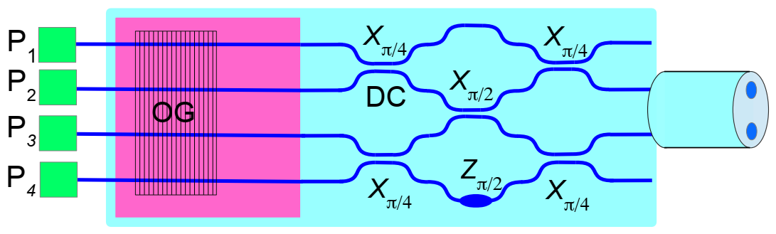
4.2.1. Quantum States Generator and Quantum Projectors On-Chip for BB84

Figure 13 shows a device to generate four quantum states, which are required in the Alice system of the BB84 protocol. It consists of four paths, that is, four ion-exchanged channel guides fabricated in a hybrid glass substrate. Moreover, an OG in the rare-earth-doped glass section (DBR lasers) generates four weak laser signals (weak coherent states) obtained with pumping beams P j , ( j = 1 , 2 , 3 , 4 ), whereas in the passive glass section four directional couplers X π / 4 and one coupler X π / 2 along with a phase shifter Z π / 2 generate the four states required for BB84 protocol at the outputs 2 and 3, namely, the 1-qubits ( 1 / 2 ) ( | 1 2 + e i δ | 1 3 ) , with δ = ± π / 2 , π , 0 . The pumping beams P j are activated in a random way, and moreover, as shown later, the device (Alice device) emits each of the four states through the outputs of paths 2 and 3 with a probability equal to 50%.
For example, if a weak coherent state is excited in channel waveguide 1 with pumping beam P 1 , then it is obtained | L   | 1 1 . Next, the concatenated couplers X π / 4 and X π / 2 along with the shifter Z π / 2 (see Figure 13) perform a linear transformation, therefore, by taking into account Equation (5) for θ = π / 4 and θ = π / 2 and Equation (7) for Φ = π / 2 , the following output state is obtained
| L 1   = 1 2 ( | 1 1 i | 1 4 ) + i 2 ( | 1 2 + i | 1 3 )
Note that in channel guides 2 and 3 we have one of the states of the BB84 protocol, that is, in a vector form we have the state ( 1 / 2 ) ( 1 , i ) t , with t indicating transposed. The other three states are obtained by using the other pumping beams. All of them are produced with a 50% of probability what is reasonable for quantum key distributions.
On the other hand, the passive part of this device (the blue section, that is, without the active section where the OG is placed) is a quantum projector for the above states. Indeed, by considering that the inputs are the channel guides 1 and 3, then the first two couplers X π / 4 and the coupler X π / 2 make a state division. The next upper coupler X π / 4 projects the states ( 1 / 2 ) ( 1 , ± 1 ) t , whereas the phase shifter and the bottom coupler X π / 4 Z π / 2 project the states ( 1 / 2 ) ( 1 , ± i ) t . This means that the device (Bob device) produces a random choice of bases. For example, let us consider the state ( 1 / 2 ) ( | 1 1 + | 1 3 ) ( 1 / 2 ) ( 1 , 1 ) t , then, the final state is
| L 1   = 1 2 | 1 2   + 1 2 e i π / 4 | 1 3   + 1 2 e i π / 4 | 1 4
Note that if the state chooses the channel 1 and 2, then it is projected on the output 2 ( | 1 2 ). If the input state is ( 1 / 2 ) ( | 1 1 | 1 3 ) ( 1 / 2 ) ( 1 , 1 ) t , then we obtain
| L 1   = i 2 | 1 1   1 2 e i π / 4 | 1 3   + 1 2 e i π / 4 | 1 4
namely, the state is projected on the output 1 ( | 1 1 ). The same procedure can be followed for the states ( 1 / 2 ) ( | 1 1 ± i | 1 3 ) ( 1 / 2 ) ( 1 , ± i ) t which are projected on the outputs 3 and 4.

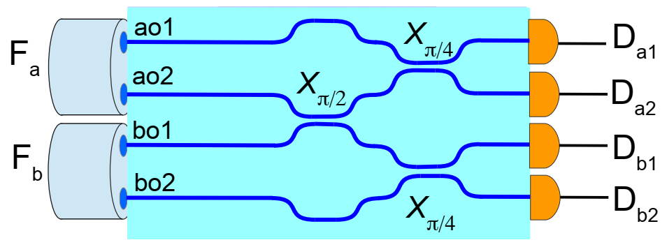
4.2.2. Bell States Measurement Integrated Device for MDI

Another interesting quantum passive device is a Bell states measurement device, which can be required in many optical quantum systems, e.g., in a MDI quantum cryptography system [217] in multicore optical fibers or few-mode optical fibers. This device can be implemented with integrated channel guides as shown next.
In Figure 14 a sketch of this device is given for the case of two multicore optical fibers F a and F b , where only two cores are shown. We must recall that multicore optical fibers and few-mode optical fibers allow for the increase of the optical transmission capability, therefore the use of these optical fibers for quantum communications is highly likely. Accordingly, the study of quantum operations with this kind of fiber also has a major potential interest. The Bell projector can be implemented by a X π / 2 coupler and two X π / 4 couplers. Indeed, let us consider the following biphoton (or 2-qubit) Bell states, according to the notation used in Figure 14,
Ψ ± = 1 2 ( | 1 a o 1 1 b o 2 ±   | 1 a o 2 1 b o 1 )
By applying the optical transformations produced by X π / 2 and X π / 4 couplers for single-photon states given by Equations (5) and (6) one obtains
Ψ + i 2 ( | 1 a 1 1 b 1 +   | 1 a 2 1 b 2 ) , Ψ 1 2 ( | 1 a 1 1 b 2 +   | 1 a 2 1 b 1 )
Thus, when photons are registered in detectors D a 1 , D b 1 or D a 2 , D b 2 (photon coincidences) we have the Bell state Ψ + , and when photons are registered in detectors D a 1 , D b 2 or D a 2 , D b 1 we have the Bell state Ψ . In short, an integrated Bell projector device has been obtained for Bell states Ψ ± .
On the other hand, this result has also an important impact in cryptography, in particular in a MDI quantum cryptography system. Indeed, let us consider the biphoton state | 1 a o 1 1 b o 2 launched by Alice and Bob, then the output state is given by
| L = 1 2 { ( | 1 a 1 1 b 2 ( | 1 a 2 1 b 1 ) + i ( | 1 a 1 1 b 1 +   | 1 a 2 1 b 2 ) } 1 2 ( Ψ + i Φ + )
that is, Bell states are again detected by photon concidences (Charlie device). Now, if the state launched by Alice and Bob is | 1 a o 2 1 b o 1 , the result is the same, except the sign: ( 1 / 2 ) ( Ψ + i Φ + ) ; therefore, a quantum key distribution is possible because Eve is not able to know which state has been sent, that is, | 1 a o 1 1 b o 2 or | 1 a o 2 1 b o 1 .
The above examples (quantum states generator and quantum projectors for BB84 and a Bell states measurement device) have made clear the potential of the integrated optical devices for the implementation of quantum operations. Next, we show how the practical implementation of these devices in a ion-exchanged glass platform is possible because only a few qubits (or qudits) are required.

4.3. Fabrication and Characterization of a Quantum Projector

We present the fabrication of the basic units X π / 4 and X π / 2 , that is, 2 × 2 directional couplers in glass, by using two consecutive purely thermal K + /Na + ion-exchange processes in glass. The first process is a selective ion exchange, that is, it is produced only in non-masked regions that corresponds to the channel waveguides defining the integrated optical component, while the second one is only a burial process through the same mask [194]. We must underline that this two-step process is different from the one proposed in Reference [199] where two consecutive K + /Na + ion exchanges are made, but the second is a planar ion exchange. Rigorously, the second step (burial process) would not be necessary but presents two important advantages. On the one hand, the modal field is located further from the glass surface, which can present irregularities, and therefore surface losses are reduced, and, on the other hand, it decreases the typical anisotropy in K + /Na + waveguides produced by mechanical stress due to the size difference of the two ions, one of the main drawback of these integrated guides. Of course there are many other strategies for fabricating directional couplers by K + /Na + ion exchange (see, for example [16,200,201]), which could also be suitable for this kind of applications. Another approach would be to use ion-exchanged MMI couplers based on multimode interference [223,224], which would have less stringent lithographic requirements. There are also proposals of reconfigurable integrated elements as directional couplers by thermo-optic modulation [225], a strategy that can be oriented to reconfigure quantum operations. In another work, an interesting design of asymmetric Y-branch waveguides for bidirectional transmission on PCB (printed circuit board) was described [226], which would allow us to join IQP and microelectronics.
The fabrication strategy presented here has given excellent experimental results for X π / 4 and X π / 2 directional couplers with both low losses and anisotropic effects (coupling between TE and TM guided modes, one of the drawbacks of K + /Na + ion exchange) thanks to the burial process. The starting point has been to use previous results [54,64,201,207,227], which have allowed us to establish a fixed temperature T = 400 ° C for both the first and the second (burial) ion exchange in a soda-lime glass with index n s = 1.5104 at λ o = 633 nm . Several tests of planar thermal ion exchange in the same type of glass substrate were made, and the effective indices of the different guided modes were measured by prism coupling method in an automated system (Metricon, Model 2010/M). From this empiric calibration and taking into account numerical results by using the EIM for channel guides, a diffusion time for the first exchange equal to t 1 = 30 min and a time t 2 = 10 min for the burial process were fixed in order to achieve single-mode channel waveguides.
In order to design and fabricate integrated quantum optical projectors, a prior optical characterization of the full fabrication process of the basic elements (the directional couplers as X π / 4 and X π / 2 ) was needed. A series of masks on the same substrate for different directional couplers have been made by changing the separation s between channel guides and the coupling length l of the couplers (a sketch of the directional coupler is shown in Figure 15), while keeping the width of the channel guides constant ( w = 3 μm). The connection between channel guides have been made through curves following the profile used by Minford et al. (MC curve) [62]. The separations and the coupling lengths chosen, after the photo-reduction process, are found in the interval s [ 3 , 6 ]   μ m and l [ 0.5 , 2 ]   mm , respectively. We must indicate that under the ion-exchange process, the lateral diffusion increases the width of the channel guides up to 4   μ m with respect to the designed mask width of 3   μ m .
An optical characterization of the directional couplers was then made. We denote as c o 1 and c o 2 , respectively, the input complex amplitudes at the two guides of the coupler and as c 1 and c 2 the corresponding output complex amplitudes, so that the output powers are P i = | c i | 2 , i = 1 , 2 . In the tests, light was coupled to one of the branches of the coupler and the power at each output was measured. Experimental results are shown in Table 1. Some important conclusions can be obtained from the results shown in Table 1: the coupler ( s , l ) = ( 3.0 , 2.0 ) is very close to a X π / 2 coupler, and the coupler ( s , l ) = ( 6.0 , 1.5 ) is very close to a X π / 4 coupler.
Alternatively, one can use a numerical linear fitting to obtain the optimal values of ( s , l ) for fabricating a particular coupler X θ ; thus, Figure 16 shows the linear fit θ ( l ) = a l + b for the three separations s considered. The term θ ( 0 ) is the coupling introduced by the Minford curves and it is different from zero because l is the distance between the curved sections. Note that the above fit allows us to define an effective length l eff such that θ ( l eff ) = κ l eff , where κ is the coupling coefficient ( a κ ), and thus we can write the following relationship
θ ( l ) = κ l + θ ( 0 )
By deriving κ and θ ( 0 ) from the linear fit of the experimental coupling results we obtain the effective length l eff = l + θ ( 0 ) / κ . In short, we have found the empiric parameters for fabricating simultaneously X π / 2 and X π / 2 couplers and thus to fabricate the three IQP devices described in the above subsection. The phase shifter π / 2 could be implemented by changing in an adiabatic way the length or the width of a channel guide.
The experimental results for the directional coupler ( s , l ) = ( 6.0 , 1.5 ) ( X π / 4 coupler) as a quantum projector can now be shown. The test was made by using a He-Ne laser source, so that we made a semi-classical optical characterization with coherent states, which is sufficient to characterize the directional coupler; we must stress, however, that with single-photon states the same results would be obtained. We excited different states at the input of the directional coupler by using an optical grating [194]. Indeed, let us consider an external optical grating with a periodic structure along the y axis (see, for instance, Figure 15). When it is normally illuminated by a Gaussian beam propagating along z direction, and the diffracted light is collected by a lens, then the diffraction orders ± 1 can be coupled to the inputs c o 1 and c o 2 of the directional coupler shown in Figure 15. Next, by translating the optical grating along y axis, different relative phases δ between the amplitudes are obtained; in other words, the following input vector of amplitudes is obtained at the directional coupler: v o t = ( c o 1 , e i δ c o 2 ) t , where superscript t stands for transposed. It is worth writing the corresponding input quantum state, i.e., the bimode coherent state | c o 1 e i δ c o 2 . Next, we choose the directional coupler ( s , l ) = ( 6.0 , 1.5 ) , which is very close to a X π / 4 coupler and therefore is a projector of quantum states ( 1 / 2 ) ( | 1 1 ± i | 1 2 ) . Alternatively, the device formed by an optical grating introducing a π / 2 phase plus a directional coupler X π / 4 can be formally regarded as a projector for states ( 1 / 2 ) ( | 1 1 ± | 1 2 ) . Note that if we use an active optical grating implemented by a spatial light modulator introducing 0 or π / 2 in a random way we have a quantum states detection system (Bob) of random bases.
In Figure 17, the experimental results (image of waveguide outputs) for these projections are shown, with the corresponding input coherent states. Note that the bimode coherent states | α / 2 ± i α / 2 are projected in states | α 0 and | 0 α , therefore single photon states ( 1 / 2 ) ( | 1 1 ± i | 1 2 ) , will be projected in states | 1 1 and | 1 2 , respectively. On the other hand, the following two-mode coherent states | α / 2 ± α / 2 do not undergo transformations, therefore the single photon states ( 1 / 2 ) ( | 1 1 ± | 1 2 ) also do not, and consequently it is also experimentally proved that they are eigenstates. This last case is highly interesting to implement a quantum random number generator.
In short, the experimental results achieved with the directional coupler confirm that a X π / 4 transformation is implemented, and therefore a projection operation can be made. A similar experimental study has been made with the X π / 2 coupler. Therefore, when several couplers X π / 4 and X π / 2 are combined, that is, couplers ( s , l ) = { ( 6.0 , 1.5 ) , ( 3.0 , 2.0 ) } fabricated simultaneously, the devices described in Section 4.2 can be fabricated and also more general projectors (high-dimensional projectors, Bell states projectors, …) by using ion exchange in glass.

5. Conclusions

In this work we have presented a review on active and quantum integrated photonic elements fabricated by ion exchange in glass, which have a remarkable impact in different fields such as classical and quantum optical communications, optical processing and optical sensing. Ion-exchanged components in rare-earth-doped glasses provide an optimal solution to implement integrated optical lasers and amplifiers; erbium-doped waveguide amplifiers represent a very important element in optical transmission systems. Likewise, a growing interest has emerged for the use of the ion-exchanged waveguide technology as an effective platform for integrated quantum photonics. We have reported theoretical and experimental results showing the high potentiality of this platform for developing active and integrated quantum devices, with particular reference to the combination of active and passive ion-exchanged glass elements in hybrid glasses. Thus, we have shown how to implement, for example, an active integrated quantum states generator device for quantum cryptography (Alice device) and passive devices such as, for example, an integrated quantum projector, suitable also for the BB84 protocol in quantum cryptography (Bob device), which allows us to detect quantum states by projective measurements, and a Bell states measurement device for MDI protocol in quantum cryptography (Charlie device). As an overall, we have shown that ion exchange in glass, even if being a very ancient technology, is still crucial for today’s (and future) photonic and quantum integration technology.

Author Contributions

The authors contributed equally to the manuscript. Both have read and agreed to the published version of the manuscript.

Funding

This research was funded by Xunta de Galicia, Consellería de Educación, Universidades e FP, Grant GRC Number ED431C2018/11.

Data Availability Statement

Data is contained within the article.

Conflicts of Interest

The authors declare no conflict of interest.

Abbreviations

The following abbreviations are used in this manuscript:
ASAluminosilicate
ASEAmplified Spontaneous Emission
BB84Bennett and Brassard 1984
CMOSComplementary Meta Oxide Semiconductor
DCDirectional Coupler
EDFAEr-Doped Fiber Amplifier
EDWAErbium-Doped Waveguide Amplifier
EYDWAErbium-Ytterbium-Doped Waveguide Amplifier
EOCBElectro-Optical Circuit Board
FMFFew-Mode Optical Fiber
IExGIon-Exchanged Glass
IQPIntegrated Quantum Photonics
MCMinford et al. Curve
MCFMulticore Optical Fiber
MDIMeasurement Device Independent
MMIMulti-Mode Interference
MUBsMutually Unbiased Bases
NLONonlinear optics
OGOptical Grating
PCBPrinted Circuit Board
PECVDPlasma-Enhanced Chemical Vapor Deposition
REDRare-Earth Doped
SPDCSpontaneous Parametric Down-Conversion)
SLSoda–Lima–silicate
WDMWavelength Division Multiplexing

References

  1. Pezzella, S. Il Trattato di Antonio da Pisa Sulla Fabbricazione Delle Vetrate Artistiche; Umbria Edizioni: Perugia, Italy, 1976. [Google Scholar]
  2. Schulze, G. Versuche über die diffusion von silber in glas. Angew. Physik 1913, 40, 335–367. [Google Scholar] [CrossRef]
  3. Righini, G.C.; Pelli, S. 1969–2019: 50 Years of Integrated Optics; Integrated Optics; Righini, G.C., Ferrari, M., Eds.; The IET: London, UK, 2020; Volume 1, pp. 1–38. [Google Scholar]
  4. Izawa, T.; Nakagome, H. Optical waveguide formed by electrically induced migration of ions in glass plates. Appl. Phys. Lett. 1972, 21, 584–586. [Google Scholar] [CrossRef]
  5. Giallorenzi, T.G.; West, E.J.; Kirk, R.; Ginther, R.; Andrews, R.A. Optical waveguides formed by thermal migration of ions in glass. Appl. Opt. 1973, 12, 1240–1245. [Google Scholar] [CrossRef]
  6. Koizumi, K.; Sumimoto, T.; Matsushita, S.; Furukawa, M. Ion Exchange Process for Manufacturing Integrated Optical Circuits. U.S. Patent N. 3,857,689, 31 December 1974. [Google Scholar]
  7. Sumimoto, T.; Matsushita, S.; Yamazaki, T.; Fujiwara, T.; Koizumi, K. Method for Manufacturing Optical Integrated Circuits Utilizing an External Electric Field. U.S. Patent N. 3,836,348A, 17 September 1974. [Google Scholar]
  8. Najafi, S.I. (Ed.) Glass Integrated Optics and Optical Fiber Devices; Number CR53 in Critical Reviews of Optical Science and Technology; SPIE: Bellingham, WA, USA, 1994. [Google Scholar]
  9. Kita, H.; Kitano, I.; Uchida, T.; Furukawa, M. Light-Focusing Glass Fiber and Rods. J. Am. Ceram. Soc. 1971, 54, 321. [Google Scholar] [CrossRef]
  10. Ohmi, S.; Sakai, H.; Asahara, Y.; Nakayama, S.; Yoneda, Y.; Izumitani, T. Gradient-index rod lens made by a double ion-exchange process. Appl. Opt. 1988, 27, 496–499. [Google Scholar] [CrossRef]
  11. Liñares, J.; Montero, C.; Prieto, X. Graded-index bifocal spectacle lenses produced by ion-exchange in glass: Paraxial designing. Pure Appl. Opt. 1995, 4, 695–699. [Google Scholar] [CrossRef]
  12. Gomez-Reino, C.; Perez, M.; Bao, C.; Flores-Arias, M. Design of GRIN optical components for coupling and interconnects. Laser Photonics Rev. 2008, 2, 203–215. [Google Scholar] [CrossRef]
  13. Graydon, O. Graded lens surprise. Nat. Photonics 2019, 13, 732. [Google Scholar] [CrossRef]
  14. Findakly, T. Glass waveguides by ion-exchange: A review. Opt. Engin. 1985, 24, 244–250. [Google Scholar] [CrossRef]
  15. Ramaswamy, R.V.; Srivastava, R. Ion-exchanged glass waveguides: A review. J. Light. Technol. 1988, 6, 984–1000. [Google Scholar] [CrossRef]
  16. Najafi, S.I. Introduction to Glass Integrated Optics; Artech House: Boston, MA, USA, 1986. [Google Scholar]
  17. Righini, G.C.; Pelli, S. Ion exchange in glass: A mature technology for photonic devices. In Materials and Devices for Photonic Circuits II; Armenise, M.N., Ed.; SPIE: Bellingham, WA, USA, 2001; Volume 4453, pp. 93–99. [Google Scholar] [CrossRef]
  18. Honkanen, S.; West, B.R.; Yliniemi, S.; Madasamy, P.; Morrell, M.; Auxier, J.; Schulzgen, A.; Peyghambarian, N.; Carriere, J.; Frantz, J.; et al. Recent advances in ion exchanged glass waveguides and devices. Phys. Chem. Glas. 2006, 47, 110–120. [Google Scholar]
  19. Tervonen, A.; Honkanen, S.K.; West, B.R. Ion-exchanged glass waveguide technology: A review. Opt. Eng. 2011, 50, 1–16. [Google Scholar] [CrossRef] [Green Version]
  20. Righini, G.C.; Chiappini, A. Glass optical waveguides: A review of fabrication techniques. Opt. Eng. 2014, 53, 071819. [Google Scholar] [CrossRef]
  21. Fernandez, T.; Sakakura, M.; Eaton, S.; Sotillo, B.; Siegel, J.; Solis, J.; Shimotsuma, Y.; Miura, K. Bespoke photonic devices using ultrafast laser driven ion migration in glasses. Prog. Mater. Sci. 2018, 94, 68–113. [Google Scholar] [CrossRef]
  22. Grelin, J.; Ghibaudo, E.; Broquin, J.E. Study of deeply buried waveguides: A way towards 3D integration. Mater. Sci. Eng. B 2008, 149, 185–189. [Google Scholar] [CrossRef]
  23. Pei, C.; Wang, G.; Yang, B.; Yang, L.; Hao, Y.; Jiang, X.; Yang, J. Study of selectively buried ion-exchange glass waveguides using backside masking. Chin. Opt. Lett. 2015, 13, 021301. [Google Scholar]
  24. Zhang, L.; Guo, X. Thermal history and its implications: A case study for ion exchange. J. Am. Ceram. Soc. 2020, 103, 3971–3977. [Google Scholar] [CrossRef]
  25. Jordan, E.; Geoffray, F.; Bouchard, A.; Ghibaudo, E.; Broquin, J.E. Development of Tl+/Na+ ion-exchanged single-mode waveguides on silicate glass for visible-blue wavelengths applications. Ceram. Int. 2015, 41, 7996–8001. [Google Scholar] [CrossRef]
  26. Liñares, J.; Montero, C.; Sotelo, D. Theory and design of an integrated optical sensor based on planar waveguiding lenses. Opt. Commun. 2000, 180, 29–36. [Google Scholar] [CrossRef]
  27. Barral, D.; Liñares-Beiras, J.; Montero-Orille, C.; Moreno, V.; Prieto-Blanco, X.; Grazu, V.; Sánchez, C.; Seara, R. Integrated Ion-Exchanged Glass Bimodal Optical Biosensor based on Modal Interference Imaging. In Proceedings of the IX Optoelectronics Spanish Meeting OPTOEL 2015, Salamanca, Spain, 13–15 July 2015; p. PO–SII–35, ISBN 978-84-606-9716-9. [Google Scholar]
  28. Asquini, R.; Buzzin, A.; Caputo, D.; de Cesare, G. Integrated Evanescent Waveguide Detector for Optical Sensing. IEEE Trans. CPMT 2018, 8, 1180–1186. [Google Scholar] [CrossRef]
  29. Du, B.; Tong, Z.; Mu, X.; Xu, J.; Liu, S.; Liu, Z.; Cao, W.; Qi, Z.M. A Potassium Ion-Exchanged Glass Optical Waveguide Sensor Locally Coated with a Crystal Violet-SiO2 Gel Film for Real-Time Detection of Organophosphorus Pesticides Simulant. Sensors 2019, 19, 4219. [Google Scholar] [CrossRef] [PubMed] [Green Version]
  30. Mamtmin, G.; Abdurahman, R.; Yan, Y.; Nizamidin, P.; Yimit, A. A highly sensitive and selective optical waveguide sensor based on a porphyrin-coated ZnO film. Sen. Actuators A 2020, 309, 111918. [Google Scholar] [CrossRef]
  31. Liu, L.; Zhou, X.; Wilkinson, J.S.; Hua, P.; Song, B.; Shi, H. Integrated optical waveguide-based fluorescent immunosensor for fast and sensitive detection of microcystin-LR in lakes: Optimization and Analysis. Sci. Rep. 2017, 7, 3655. [Google Scholar] [CrossRef] [PubMed] [Green Version]
  32. Nikonorov, N.V.; Petrovskii, G.T. Ion-exchanged glasses in integrated optics: The current state of research and prospects (a review). Glass Phys. Chem. 1999, 25, 16–55. [Google Scholar]
  33. Opilski, A.; Rogozinski, R.; Gut, K.; Blahut, M. Aspects of application of ion exchange in glass. In Lightguides and Their Applications; Wojcik, J., Wojcik, W., Eds.; SPIE: Bellingham, WA, USA, 2000; Volume 4239, pp. 1–10. [Google Scholar] [CrossRef]
  34. Jackel, J.L.; Vogel, E.M.; Aitchison, J.S. Ion-exchanged optical waveguides for all-optical switching. Appl. Opt. 1990, 29, 3126–3129. [Google Scholar] [CrossRef]
  35. Roussignol, P.; Ricard, D.; Flytzanis, C. Nonlinear optical properties of commercial semiconductor doped glasses. Appl. Phys. A 1987, 44, 285–292. [Google Scholar] [CrossRef]
  36. Lawandy, N.M.; MacDonald, R.L. Optically encoded phase-matched second-harmonic generation in semiconductor-microcrystallite-doped glasses. JOSA B 1991, 8, 1307–1314. [Google Scholar] [CrossRef]
  37. Righini, G.; Pelli, S.; Blasi, C.D.; Fagherazzi, G.; Manno, D. Ion-exchanged waveguides in semiconductor-doped glasses. In Glasses for Optoelectronics II; SPIE: Bellingham, WA, USA, 1991; Volume 1513, pp. 105–111. [Google Scholar] [CrossRef]
  38. Charlet, B.; Bastard, L.; Broquin, J.E. 1 kW peak power passively Q-switched Nd3+-doped glass integrated waveguide laser. Opt. Lett. 2011, 36, 1987–1989. [Google Scholar] [CrossRef]
  39. Geoffray, F.; Bastard, L.; Broquin, J.E. High confinement ion-exchanged waveguides for nonlinear applications. Ceram. Int. 2015, 41, 8034–8039. [Google Scholar] [CrossRef]
  40. Legrand, L.; Bouchard, A.; Grosa, G.; Broquin, J.E. Hybrid integration of 300 nm-thick LiNbO3 films on ion-exchanged glass waveguides for efficient nonlinear integrated devices. In Integrated Optics: Devices, Materials, and Technologies XXII; García-Blanco, S.M., Cheben, P., Eds.; SPIE: Bellingham, WA, USA, 2018; Volume 10535, pp. 44–50. [Google Scholar] [CrossRef]
  41. Editorial. The rise of integrated quantum photonics. Nat. Photonics 2020, 14, 265. [Google Scholar] [CrossRef]
  42. Politi, A.; Crya, M.J.; Rarity, J.G.; Yu, S.; O’Brien, J.L. Silica-on-silicon waveguide quantum circuits. Science 2008, 320, 646–649. [Google Scholar] [CrossRef] [Green Version]
  43. Politi, A.; Matthews, J.C.F.; Thompson, M.G.; O’Brien, J.L. Integrated Quantum Photonics. IEEE J. Sel. Top. Quantum Electron. 2009, 15, 1673–1684. [Google Scholar] [CrossRef] [Green Version]
  44. Bogdanov, S.; Shalaginov, M.Y.; Boltasseva, A.; Shalaev, V.M. Material platforms for integrated quantum photonics. Opt. Mater. Express 2017, 7, 111–132. [Google Scholar] [CrossRef]
  45. Wang, J.; Sciarrino, F.; Laing, A.; Thompson, M. Integrated photonic quantum technologies. Nat. Photonics 2020, 14, 273–284. [Google Scholar] [CrossRef]
  46. Smith, D.H.; Mennea, P.L.; Gates, J.C. Integrated quantum photonics. In Integrated Optics; Righini, G.C., Ferrari, M., Eds.; The Institution of Engineering and Technology: London, UK, 2021; Volume 2, pp. 337–359. [Google Scholar]
  47. Elshaari, A.W.; Pernice, W.; Srinivasan, K.; Benson, O.; Zwiller, V. Hybrid integrated quantum photonic circuits. Nat. Photonics 2015, 14, 285–298. [Google Scholar] [CrossRef]
  48. Meany, T.; Gräfe, M.; Heilmann, R.; Perez-Leija, A.; Gross, S.; Steel, M.J.; Withford, M.J.; Szameit, A. Laser written circuits for quantum photonics. Laser Photonics Rev. 2015, 9, 363–384. [Google Scholar] [CrossRef] [Green Version]
  49. Liñares, J.; Nistal, M.C.; Barral, D.; Moreno, V.; Montero, C.; Prieto, X. Quantum Integrated Optics: Theory and Applications. Opt. Pura Apl. 2011, 44, 241–253. [Google Scholar]
  50. Xia, C.; Amezcua-Correa, R.; Bai, N.; Antonio-Lopez, E.; May-Arrioja, D.; Schulzgen, A.; Richardson, M.; Liñares, J.; Montero, C.; Mateo, E.; et al. Hole-Assisted Few-Mode Multicore Fiber for High-Density Space-Division Multiplexing. IEEE Photonics Technol. Lett. 2012, 24, 1914–1917. [Google Scholar] [CrossRef]
  51. Balado, D.; Liñares, J.; Prieto-Blanco, X.; Barral, D. Phase and polarization autocompensating N-dimensional quantum cryptography in multicore optical fibers. JOSA B 2019, 36, 2793–2803. [Google Scholar] [CrossRef]
  52. Bai, N.; Ip, E.; Huang, Y.K.; Mateo, E.; Yaman, F.; Li, M.J.; Bickham, S.; Ten, S.; Liñares, J.; Montero, C.; et al. Mode-division multiplexed transmission with inline few-mode fiber amplifier. Opt. Express 2012, 20, 2668–2680. [Google Scholar] [CrossRef] [Green Version]
  53. Li, G.; Winick, K.A.; Griffin, H.C.; Hayden, J.S. Systematic modeling study of channel waveguide fabrication by thermal silver ion exchange. Appl. Opt. 2006, 45, 1743–1755. [Google Scholar] [CrossRef] [PubMed]
  54. Prieto-Blanco, X.; Liñares, J. Two-Mode Waveguide Characterization by Intensity Measurements from Exit Face Images. IEEE Photonics J. 2012, 4, 65–79. [Google Scholar] [CrossRef]
  55. Righini, G.C.; Pelli, S.; Ferrari, M.; Armellini, C.; Zampedri, L.; Tosello, C.; Ronchin, S.; Rolli, R.; Moser, E.; Montagna, M.; et al. Er-doped silica-based waveguides prepared by different techniques: RF-sputtering, sol-gel and ion-exchange. Opt. Quantum Electron. 2002, 34, 1151–1166. [Google Scholar] [CrossRef]
  56. Luff, B.J.; Harris, R.D.; Wilkinson, J.S.; Wilson, R.; Schiffrin, D.J. Integrated-optical directional coupler biosensor. Opt. Lett. 1996, 21, 618–620. [Google Scholar] [CrossRef] [Green Version]
  57. Tepper, J.; Labadie, L.; Diener, R.; Minardi, S.; Pott4, J.U.; Thomson, R.; Nolte, S. Integrated optics prototype beam combiner for long baseline interferometry in the L and M bands. Astron. Astrophys. 2017, 602, A66-1–A66-8. [Google Scholar] [CrossRef] [Green Version]
  58. Conzone, S.D.; Hayden, J.S.; Funk, D.S.; Roshko, A.; Veasey, D.L. Hybrid glass substrates for waveguide device manufacture. Opt. Lett. 2001, 26, 509–511. [Google Scholar] [CrossRef]
  59. Hayden, J.S.; Simpson, R.D.; Conzone, S.D.; Hickernell, R.K.; Callicoatt, B.; Roshko, A.; Sanford, N.A. Passive and active characterization of hybrid glass substrates for telecommunication applications. In Rare-Earth-Doped Materials and Devices VI; Jiang, S., Keys, R.W., Eds.; International Society for Optics and Photonics, SPIE: Bellingham, WA, USA, 2002; Volume 4645, pp. 43–50. [Google Scholar] [CrossRef]
  60. Casale, M.; Bucci, D.; Bastard, L.; Broquin, J.E. Hybrid erbium-doped DFB waveguide laser made by wafer bonding of two ion-exchanged glasses. Ceram. Int. 2015, 41, 7466–7470. [Google Scholar] [CrossRef]
  61. Blaize, S.; Bastard, L.; Cassagnetes, C.; Broquin, J.E. Multiwavelengths DFB waveguide laser arrays in Yb-Er codoped phosphate glass substrate. IEEE Photonics Technol. Lett. 2003, 15, 516–518. [Google Scholar] [CrossRef]
  62. Minford, W.J.; Korotky, S.K.; Alferness, R.C. Low-Loss Ti:LiNbO3 Waveguide Bends at λo = 1.3 μm. IEEE J. Quantum Electron. 1982, QE-18, 1802–1906. [Google Scholar] [CrossRef]
  63. Pelli, S.; Righini, G.C.; Scaglione, A.; Yip, G.L.; Noutsios, P.C.; Braeuer, A.H.; Dannberg, P.; Linares, J.; Reino, C.R.; Mazzi, G.; et al. Testing of optical waveguides (TOW) cooperative project: Preliminary results of the characterization of k-exchanged waveguides. In Linear and Nonlinear Integrated Optics; Righini, G.C., Yevick, D., Eds.; SPIE: Bellingham, WA, USA, 1994; Volume 2212, pp. 126–131. [Google Scholar] [CrossRef]
  64. Liñares, J.; Prieto, X.; Montero, C. A Novel Refractive Index Profile for Optical Characterization of Nonlinear Diffusion Processes and Planar Waveguides in Glass. Opt. Mater. 1994, 3, 229–236. [Google Scholar] [CrossRef]
  65. Sebastiani, S.; Berneschi, S.; Brenci, M.; Nunzi-Conti, G.; Pelli, S.; Righini, G.C. Simple approach to calculate the refractive index profile of ion-exchanged waveguides. Opt. Eng. 2005, 44, 1–5. [Google Scholar] [CrossRef]
  66. Liñares, J.; Moreno, V.; Nistal, M.C.; Salgueiro, J.R. Modelling of ion-exchanged monomode channel guides with quasi-exact modal solutions by the effective index method. J. Mod. Opt. 2001, 48, 789–795. [Google Scholar] [CrossRef]
  67. Araujo, R. Interdiffusion in a one-dimensional interacting system. J. Non-Cryst. Solids 1993, 152, 70–74. [Google Scholar] [CrossRef]
  68. Tervonen, A. A general model for fabrication processes of channel waveguides by ion exchange. J. Appl. Phys. 1990, 67, 2746–2752. [Google Scholar] [CrossRef]
  69. Salmio, R.; Saarinen, J.; Turunen, J.; Tervonen, A. Graded-index diffractive elements by thermal ion exchange in glass. Appl. Phys. Lett. 1995, 66, 917–919. [Google Scholar] [CrossRef]
  70. Prieto, X.; Liñares, J. Increasing resistivity effects in field-assisted ion exchange for planar optical waveguide fabrication. Opt. Lett. 1996, 21, 1363–1365. [Google Scholar] [CrossRef]
  71. Prieto-Blanco, X. Electro-diffusion equations of monovalent cations in glass under charge neutrality approximation for optical waveguide fabrication. Opt. Mater. 2008, 31, 418–428. [Google Scholar] [CrossRef]
  72. Liñares, J.; Prieto-Blanco, X.; Carral, G.M.; Nistal, M.C. Quantum Photonic Simulation of Spin-Magnetic Field Coupling and Atom-Optical Field Interaction. Appl. Sci. 2020, 10, 8850. [Google Scholar] [CrossRef]
  73. Hanzawa, N.; Saitoh, K.; Sakamoto, T.; Matsui, T.; Tomita, S.; Koshiba, M. Demonstration of mode-division multiplexing transmission over 10 km two-mode fiber with mode coupler. In Proceedings of the 2011 Optical Fiber Communication Conference, Los Angeles, CA, USA, 6–10 March 2011; pp. 1–3. [Google Scholar]
  74. Snitzer, E. Optical maser action of Nd3+ in a barium crown glass. Phys. Rev. Lett. 1961, 7, 444. [Google Scholar] [CrossRef]
  75. Koester, C.J.; Snitzer, E. Amplification in a fiber laser. Appl. Opt. 1964, 3, 1182–1186. [Google Scholar] [CrossRef]
  76. Yajima, H.; Kawase, S.; Sekimoto, Y. Amplification at 1.06 μm using a Nd: Glass thin-film waveguide. Appl. Phys. Lett. 1972, 21, 407–409. [Google Scholar] [CrossRef]
  77. Saruwatari, M.; Izawa, T. Nd-glass laser with three-dimensional optical waveguide. Appl. Phys. Lett. 1974, 24, 603–605. [Google Scholar] [CrossRef]
  78. Najafi, S.I.; Wang, W.; Currie, J.F.; Leonelli, R.; Brebner, J.L. Fabrication and characterization of neodymium-doped glass waveguides. IEEE Photonics Technol. Lett. 1989, 1, 109–110. [Google Scholar] [CrossRef]
  79. Aoki, H.; Maruyama, O.; Asahara, Y. Glass waveguide laser. IEEE Photonics Technol. Lett. 1990, 2, 459–460. [Google Scholar] [CrossRef]
  80. Aoki, H.; Ishikawa, E.; Asahara, Y. Nd3+-doped glass waveguide amplifier at 1.054 μm. Electron. Lett. 1991, 27, 2351–2353. [Google Scholar] [CrossRef]
  81. Mwarania, E.; Reekie, L.; Wang, J.; Wilkinson, J. Low-threshold monomode ion-exchanged waveguide lasers in neodymium-doped BK-7 glass. Electron. Lett. 1990, 26, 1317–1318. [Google Scholar] [CrossRef] [Green Version]
  82. Sanford, N.A.; Malone, K.J.; Larson, D.R.; Hickernell, R.K. Y-branch waveguide glass laser and amplifier. Opt. Lett. 1991, 16, 1168–1170. [Google Scholar] [CrossRef] [PubMed]
  83. Roman, J.E.; Winick, K.A. Neodymium-doped glass channel waveguide laser containing an integrated distributed Bragg reflector. Appl. Phys. Lett. 1992, 61, 2744–2746. [Google Scholar] [CrossRef] [Green Version]
  84. Miliou, A.N.; Cao, X.F.; Srivastava, R.; Ramaswamy, R.V. 15-dB amplification at 1.06 μm in ion-exchanged silicate glass waveguides. IEEE Photonics Technol. Lett. 1993, 5, 416–418. [Google Scholar] [CrossRef]
  85. Aust, J.A.; Malone, K.J.; Veasey, D.L.; Sanford, N.A.; Roshko, A. Passively Q-switched Nd-doped waveguide laser. Opt. Lett. 1994, 19, 1849–1851. [Google Scholar] [CrossRef]
  86. Mears, R.; Reekie, L.; Jauncey, I.; Payne, D. Low-noise erbium-doped fibre amplifier operating at 1.54 μm. Electron. Lett. 1987, 23, 1026–1028(2). [Google Scholar] [CrossRef]
  87. Desurvire, E.; Simpson, J.R.; Becker, P.C. High-gain erbium-doped traveling-wave fiber amplifier. Opt. Lett. 1987, 12, 888–890. [Google Scholar] [CrossRef]
  88. Miniscalco, W.J. Erbium-doped glasses for fiber amplifiers at 1500 nm. J. Light. Technol. 1991, 9, 234–250. [Google Scholar] [CrossRef] [Green Version]
  89. Feuchter, T.; Mwarania, E.K.; Wang, J.; Reekie, L.; Wilkinson, J.S. Erbium-doped ion-exchanged waveguide lasers in BK-7 glass. IEEE Photonics Technol. Lett. 1992, 4, 542–544. [Google Scholar] [CrossRef] [Green Version]
  90. Kitagawa, T.; Hattori, K.; Shuto, K.; Yasu, M.; Kobayashi, M.; Horiguchi, M. Amplification in Erbium-doped silica-based planar lightwave circuits. Optical Amplifiers and Their Applications. Optical Society of America. Electron. Lett. 1992. [Google Scholar] [CrossRef]
  91. Yan, Y.C.; Faber, A.J.; de Waal, H.; Kik, P.G.; Polman, A. Erbium-doped phosphate glass waveguide on silicon with 4.1 dB/cm gain at 1.535 μm. Appl. Phys. Lett. 1997, 71, 2922–2924. [Google Scholar] [CrossRef] [Green Version]
  92. Polman, A. Erbium implanted thin film photonic materials. J. Appl. Phys. 1997, 82, 1–39. [Google Scholar] [CrossRef]
  93. Jansen, R.; LaBorde, P.; Lerminiaux, C.; Benveniste, C.; Hall, D. Integrated Optical Signal Amplifier. U.S. Patent N. 5,128,801, 7 July 1992. [Google Scholar]
  94. LaBorde, P. Optical Signal Amplifier Glasses. U.S. Patent N. 5,475,528, 6 March 1995. [Google Scholar]
  95. Ohtsuki, T.; Honkanen, S.; Ingenhoff, J.; Heyden, J.; Fabricius, N.; Najafi, S.I.; Peyghambarian, N. Polarization-insensitive planar glass waveguide amplifiers by silver ion exchange. In Proceedings of the Conference on Lasers and Electro-Optics, Optical Society of America, Anaheim, CA, USA, 2–7 June 1996; p. CThQ6. [Google Scholar]
  96. Delavaux, J.P.; Granlund, S.; Mizuhara, O.; Tzeng, L.D.; Barbier, D.; Rattay, M.; Andre, F.S.; Kevorkian, A. Integrated optics erbium ytterbium amplifier system in 10 Gb/s fiber transmission experiment. In Proceedings of the European Conference on Optical Communication, Oslo, Norway, 19 September 1996; Volume 1, pp. 123–126. [Google Scholar]
  97. Honkanen, S.; Laine, J.P.; Ohtsuki, T.; Tervonen, A.; Peyghambarian, N. Modeling of Er-doped ion-exchanged glass waveguide amplifiers. In Rare-Earth-Doped Devices; Honkanen, S., Ed.; SPIE: Bellingham, WA, USA, 1997; Volume 2996, pp. 103–108. [Google Scholar] [CrossRef]
  98. Barbier, D.; Rattay, M.; Saint Andre, F.; Clauss, G.; Trouillon, M.; Kevorkian, A.; Delavaux, J.P.; Murphy, E. Amplifying four-wavelength combiner, based on erbium/ytterbium-doped waveguide amplifiers and integrated splitters. IEEE Photonics Technol. Lett. 1997, 9, 315–317. [Google Scholar] [CrossRef]
  99. Hempstead, M. Ion-exchanged glass waveguide lasers and amplifiers. In Rare-Earth-Doped Devices; Honkanen, S., Ed.; SPIE: Bellingham, WA, USA, 1997; Volume 2996, pp. 94–102. [Google Scholar] [CrossRef] [Green Version]
  100. Shooshtari, A.; Meshkinfam, P.; Touam, T.; Andrews, M.P.; Najafi, S.I. Ion-exchanged Er/Yb phosphate glass waveguide amplifiers and lasers. Opt. Eng. 1998, 37, 1188–1192. [Google Scholar] [CrossRef]
  101. Man, S.Q.; Wong, R.S.F.; Pun, E.Y.B.; Chung, P.S. Frequency upconversion in Er3+-doped alkali bismuth gallate glasses. In Proceedings of the 1999 IEEE LEOS Annual Meeting Conference, (Cat. No.99CH37009). San Francisco, CA, USA, 8–11 November 1999; Volume 2, pp. 812–813. [Google Scholar] [CrossRef]
  102. Peters, P.M.; Funk, D.S.; Peskin, A.P.; Veasey, D.L.; Sanford, N.A.; Houde-Walter, S.N.; Hayden, J.S. Ion-exchanged waveguide lasers in Er3+-Yb3+ codoped silicate glass. Appl. Opt. 1999, 38, 6879–6886. [Google Scholar] [CrossRef]
  103. Iiyama, K.; Hongo, K.; Demura, F.; Takamiya, S. Erbium/ytterbium co-doped optical waveguide amplifier in soda-lime glass by silver ion exchange. In Proceedings of the Technical Digest, CLEO/Pacific Rim ’99, (Cat. No.99TH8464). Seoul, Korea, 30 August–3 September 1999; Volume 4, pp. 1087–1088. [Google Scholar] [CrossRef]
  104. Conti, G.N.; Ayras, P.; Cavaliere, C.; Hwang, B.C.; Luo, T.; Rantala, J.T.; Jiang, S.; Honkanen, S.; Peyghambarian, N. Strip-loaded structure for ion-exchanged Er3+-doped glass waveguide amplifiers. In Rare-Earth-Doped Materials and Devices III; Jiang, S., Honkanen, S., Eds.; SPIE: Bellingham, WA, USA, 1999; Volume 3622, pp. 122–128. [Google Scholar] [CrossRef]
  105. Araci, I.E.; Mendes, S.B.; Yurt, N.; Honkanen, S.; Peyghambarian, N. Highly sensitive spectroscopic detection of heme-protein submonolayer films by channel integrated optical waveguide. Opt. Express 2007, 15, 5595–5603. [Google Scholar] [CrossRef] [Green Version]
  106. Veasey, D.L.; Funk, D.S.; Sanford, N.A.; Hayden, J.S. Arrays of distributed-Bragg-reflector waveguide lasers at 1536 nm in Yb/Er codoped phosphate glass. Appl. Phys. Lett. 1999, 74, 789–791. [Google Scholar] [CrossRef]
  107. Shmulovich, J.; Muehlner, D.; Bruce, A.; Delavaux, J.M.; McIntosh, C.; Lenz, G.; Gomez, L.; Laskowski, E.; Paunescu, A.; Pafchek, R.; et al. Erbium-doped planar waveguide amplifiers integrated with silica waveguide technology. In Proceedings of the Optical Fiber Communication Conference, Baltimore, MD, USA, 7 March 2000; p. WA1. [Google Scholar]
  108. Hehlen, M.P.; Cockroft, N.J.; Gosnell, T.R.; Bruce, A.J. Spectroscopic properties of Er3+- and Yb3+-doped soda-lime silicate and aluminosilicate glasses. Phys. Rev. B 1997, 56, 9302–9318. [Google Scholar] [CrossRef]
  109. Vossler, G.L.; Brooks, C.J.; Winik, K.A. Planar Er:Yb glass ion exchanged waveguide laser. Electron. Lett. 1995, 31, 1162–1163. [Google Scholar] [CrossRef] [Green Version]
  110. Fournier, P.; Meshkinfam, P.; Fardad, M.A.; Andrews, M.P.; Najafi, S.I. Potassium ion-exchanged Er-Yb doped phosphate glass amplifier. Electron. Lett. 1997, 33, 293–295. [Google Scholar] [CrossRef]
  111. Camy, P.; Roman, J.E.; Willems, F.W.; Hempstead, M.; Van Der Plaats, J.C.; Prel, C.; Beguin, A.; Koonen, A.M.J.; Wilkinson, J.S.; Lerminiaux, C. Ion-exchanged planar lossless splitter at 1.5 μm. Electron. Lett. 1996, 32, 321–323. [Google Scholar] [CrossRef]
  112. Barbier, D.; Delavaux, J.M.; Kevorkian, A.; Gastaldo, P.; Jouanno, J.M. Yb/Er Integrated optics amplifiers on phosphate glass in single and double pass configurations. In Optical Fiber Communications Conference; Optical Society of America: Eindhoven, The Netherlands, 1995; p. PD3. [Google Scholar] [CrossRef]
  113. Barbier, D.; Bruno, P.; Cassagnettes, C.; Trouillon, M.; Hyde, R.L.; Kevorkian, A.; Delavaux, J.M.P. Net gain of 27 dB with a 8.6-cm-long Er/Yb-doped glass-planar-amplifier. In Proceedings of the OFC ’98, Optical Fiber Communication Conference and Exhibit, OSA Technical Digest Series Volume2 (IEEE Cat. No.98CH36177). San Jose, CA, USA, 22–27 February 1998; pp. 45–46. [Google Scholar] [CrossRef]
  114. Philipsen, J.L.; Barbier, D.; Kévorkian, A.; Cassagnettes, C.; Krebs, N.; Bruno, P. Compact gain-block consisting of an Er3+-doped waveguide amplifier (EDWA) and a pump/signal multiplexer, realized by ion exchange. In Optical Amplifiers and Their Applications; OSA: Québec, QC, Canada, 2000; p. OTuD2. [Google Scholar] [CrossRef]
  115. Martucci, A.; Guglielmi, M.; Fick, J.; Pelli, S.; Forastiere, M.A.; Righini, G.C.; Battaglin, C. Germania sol-gel waveguides for optical amplifiers. In Sol-Gel Optics V; Dunn, B.S., Pope, E.J.A., Schmidt, H.K., Yamane, M., Eds.; SPIE: Bellingham, WA, USA, 2000; Volume 3943, pp. 2–9. [Google Scholar] [CrossRef]
  116. Pelli, S.; Brenci, M.; Fossi, M.; Righini, G.C.; Duverger, C.; Montagna, M.; Rolli, R.; Ferrari, M. Optical and spectroscopic characterization of Er/Yb-activated planar waveguides. In Rare-Earth-Doped Materials and Devices IV; Jiang, S., Ed.; SPIE: Bellingham, WA, USA, 2000; Volume 3942, pp. 139–145. [Google Scholar] [CrossRef]
  117. Righini, G.C.; Pelli, S.; Fossi, M.; Brenci, M.; Lipovskii, A.A.; Kolobkova, E.V.; Speghini, A.; Bettinelli, M. Characterization of Er-doped sodium-niobium phosphate glasses. In Rare-Earth-Doped Materials and Devices V; Jiang, S., Ed.; SPIE: Bellingham, WA, USA, 2001; Volume 4282, pp. 210–215. [Google Scholar] [CrossRef] [Green Version]
  118. Sorbello, G.; Taccheo, S.; Marano, M.; Marangoni, M.; Osellame, R.; Ramponi, R.; Laporta, P. Comparative study of Ag–Na thermal and field-assisted ion exchange on Er-doped phosphate glass. Opt. Mater. 2001, 17, 425–435. [Google Scholar] [CrossRef]
  119. Kolobkobal, E.V.; Lipovskii, A.A.; Montero, C.; Liñares, J. Formation and modelling of optically waveguiding structures in a high-concentration Er-doped phosphate glass. J. Phys. D Appl. Phys. 1999, 32, L9. [Google Scholar] [CrossRef]
  120. Lin, H.; Jiang, S.; Wu, J.; Song, F.; Peyghambarian, N.; Pun, E.Y.B. Er3+-doped Na2O–Nb2O5–TeO2 glasses for optical waveguide laser and amplifier. J. Phys. Appl. Phys. 2003, 36, 812–817. [Google Scholar] [CrossRef]
  121. Conti, G.N.; Tikhomirov, V.K.; Bettinelli, M.; Berneschi, S.; Brenci, M.; Chen, B.; Pelli, S.; Speghini, A.; Seddon, A.B.; Righini, G.C. Characterization of ion-exchanged waveguides in tungsten tellurite and zinc tellurite Er3+-doped glasses. Opt. Eng. 2003, 42, 2805–2811. [Google Scholar] [CrossRef]
  122. Pelli, S.; Bettinelli, M.; Brenci, M.; Calzolai, R.; Chiasera, A.; Ferrari, M.; Nunzi Conti, G.; Speghini, A.; Zampedri, L.; Zheng, J.; et al. Erbium-doped silicate glasses for integrated optical amplifiers and lasers. J. Non-Cryst. Solids 2004, 345–346, 372–376. [Google Scholar] [CrossRef]
  123. Liu, K.; Pun, E.Y.B. K+-Na+ ion-exchanged waveguides in Er3+ -Yb3+ codoped phosphate glasses using field-assisted annealing. Appl. Opt. 2004, 43, 3179–3184. [Google Scholar] [CrossRef] [PubMed]
  124. Pissadakis, S.; Ikiades, A.; Hua, P.; Sheridan, A.K.; Wilkinson, J.S. Photosensitivity of ion-exchanged Er-doped phosphate glass using 248 nm excimer laser radiation. Opt. Express 2004, 12, 3131–3136. [Google Scholar] [CrossRef] [PubMed]
  125. Capek, P.; Mika, M.; Oswald, J.; Tresnakova, P.; Salavcova, L.; Kolek, O.; Schrofel, J.; Spirkova, J. Effect of divalent cations on properties of Er3+-doped silicate glasses. Opt. Mater. 2004, 27, 331–336. [Google Scholar] [CrossRef]
  126. Mika, M.; Kolek, O.; Spirkova, J.; Capek, P.; Berneschi, S.; Brenci, M.; Conti, G.N.; Pelli, S.; Sebastiani, S.; Righini, G.C. The effect of Ca2+, Mg2+, and Zn2+ on optical properties of Er3+-doped silicate glass. In Optical Components and Materials II; Jiang, S., Digonnet, M.J., Eds.; SPIE: Bellingham, WA, USA, 2005; Volume 5723, pp. 63–70. [Google Scholar] [CrossRef]
  127. Ondrac, F.; Ek; Salavcova, L.; Míka, M.; Špirková, J. Characterization of Erbium Doped Glass Optical Waveguides by a Fine Tunable Semiconductor Laser. Meas. Sci. Rev. 2005, 5, 6–9. [Google Scholar]
  128. Bucci, D.; Grelin, J.; Ghibaudo, E.; Broquin, J.E. Study of a pump/signal multiplexer based on a segmented asymmetric Y junction by silver/sodium ion exchange on glass. Proc. SPIE 2006, 6123, 246–254. [Google Scholar] [CrossRef]
  129. Berneschi, S.; Bettinelli, M.; Brenci, M.; Dall’Igna, R.; Nunzi Conti, G.; Pelli, S.; Profilo, B.; Sebastiani, S.; Speghini, A.; Righini, G.C. Optical and spectroscopic properties of soda-lime alumino silicate glasses doped with Er3+ +and/or Yb3+. Opt. Mater. 2006, 28, 1271–1275. [Google Scholar] [CrossRef]
  130. Yliniemi, S.; Albert, J.; Laronche, A.; Castro, J.M.; Geraghty, D.; Honkanen, S. Negligible birefringence in dual-mode ion-exchanged glass waveguide gratings. Appl. Opt. 2006, 45, 6602–6606. [Google Scholar] [CrossRef]
  131. Nandi, P.; Jose, G. Erbium doped phospho-tellurite glasses for 1.5 μm optical amplifiers. Opt. Commun. 2006, 265, 588–593. [Google Scholar] [CrossRef]
  132. Rivera, V.; Chillcce, E.; Rodriguez, E.; Cesar, C.; Barbosa, L. Planar waveguides by ion exchange in Er3+-doped tellurite glass. J. Non-Cryst. Solids 2006, 352, 363–367. [Google Scholar] [CrossRef]
  133. Sakida, S.; Nanba, T.; Miura, Y. Refractive-index profiles and propagation losses of Tb3+-doped tungsten tellurite glass waveguide by Ag+–Na+ ion-exchange. Mater. Lett. 2006, 60, 3413–3415. [Google Scholar] [CrossRef]
  134. Bucci, D.; Grelin, J.; Ghibaudo, E.; Broquin, J. Realization of a 980-nm/1550-nm Pump-Signal (De)multiplexer Made by Ion-Exchange on Glass Using a Segmented Asymmetric Y-Junction. IEEE Photonics Technol. Lett. 2007, 19, 698–700. [Google Scholar] [CrossRef]
  135. Ondráček, F.; Salavcová, L.; Míka, M.; Lahodný, F.; Slavík, R.; Špirková, J.; Čtyroký, J. Fabrication and characterization of channel optical waveguides in Er-Yb-doped silicate glasses. Opt. Mater. 2007, 30, 457–461. [Google Scholar] [CrossRef]
  136. Sakida, S.; Nanba, T.; Miura, Y. Optical properties of Er3+-doped tungsten tellurite glass waveguides by Ag-Na ion-exchange. Opt. Mater. 2007, 30, 586–593. [Google Scholar] [CrossRef]
  137. Svecova, B.; Spirkova, J.; Janakova, S.; Mika, M. Ion-exchanged optical waveguides fabricated in novel Er3+ and Er3+. Yb3+-doped silicate glasses: Relations between glass composition, basicity and waveguide properties. Mater. Sci. Eng. B 2008, 149, 177–180. [Google Scholar] [CrossRef]
  138. Barbosa, A.; Maia, L.; Nascimento, A.; Gonçalves, R.; Poirier, G.; Messaddeq, Y.; Ribeiro, S. Er3+-doped germanate glasses for active waveguides prepared by Ag or K - Na ion-exchange. J. Non-Cryst. Solids 2008, 354, 4743–4748. [Google Scholar] [CrossRef]
  139. Svecova, B.; Spirkova, J.; Janakova, S.; Mika, M.; Oswald, J.; Mackova, A. Diffusion process applied in fabrication of ion-exchanged optical waveguides in novel Er3+ and Er3+ - Yb3+-doped silicate glasses. J. Mater. Sci. Mater. Electron. 2009, 20, 510–513. [Google Scholar] [CrossRef]
  140. Yang, D.L.; Pun, E.Y.; Lin, H. Tm3+-doped ion-exchanged aluminum germanate glass waveguide for S-band amplification. Appl. Phys. Lett. 2009, 95, 151106. [Google Scholar] [CrossRef]
  141. Bozelli, J.C.; Nunes, L.A.d.O.; Sigoli, F.A.; Mazali, I.O. Erbium and Ytterbium Codoped Titanoniobophosphate Glasses for Ion-Exchange-Based Planar Waveguides. J. Am. Ceram. Soc. 2010, 93, 2689–2692. [Google Scholar] [CrossRef]
  142. Kimura, K.; Sakida, S.; Benino, Y.; Nanba, T. Fabrication and characterization of Er3+-doped tellurite glass waveguide by Ag-Na ion-exchange method. IOP Conf. Ser. Mater. Sci. Eng. 2011, 18, 112018. [Google Scholar] [CrossRef]
  143. Olivier, M.; Doualan, J.L.; Camy, P.; Lhermite, H.; Adam, J.L.; Nazabal, V. Development of Praseodymium doped fluoride waveguide. In Optical Components and Materials IX; Jiang, S., Digonnet, M.J.F., Dries, J.C., Eds.; SPIE: Bellingham, WA, USA, 2012; Volume 8257, pp. 26–32. [Google Scholar] [CrossRef]
  144. Shen, L.; Chen, B.; Lin, H.; Pun, E. Praseodymium ion doped phosphate glasses for integrated broadband ion-exchanged waveguide amplifier. J. Alloys Compd. 2015, 622, 1093–1097. [Google Scholar] [CrossRef]
  145. Wong, S.F.; Pun, E.Y.B.; Chung, P.S. Er3+-Yb3+ codoped phosphate glass waveguide amplifier using Ag-Li ion exchange. IEEE Photonics Technol. Lett. 2002, 14, 80–82. [Google Scholar] [CrossRef]
  146. Chen, H.Y.; Liu, Y.Z.; Dai, J.Z.; Yang, Y.P.; Guan, Z.G.; Huang, X.L. Er3+/Yb3+ codoped phosphate glass waveguide amplifier. In Proceedings of the IEEE 2002 International Conference on Communications, Circuits and Systems, Chengdu, China, 29 June–1 July 2002; Volume 1, pp. 827–829. [Google Scholar] [CrossRef]
  147. Jose, G.; Sorbello, G.; Taccheo, S.; Cianci, E.; Foglietti, V.; Laporta, P. Active waveguide devices by Ag–Na ion exchange on erbium–ytterbium doped phosphate glasses. J. Non-Cryst. Solids 2003, 322, 256–261. [Google Scholar] [CrossRef]
  148. Gardillou, F.; Bastard, L.; Broquin, J.E. 4.25 dB gain in a hybrid silicate/phosphate glasses optical amplifier made by wafer bonding and ion-exchange techniques. Appl. Phys. Lett. 2004, 85, 5176–5178. [Google Scholar] [CrossRef]
  149. Gardillou, F.; Broquin, J.E. Optical amplifier made by reporting an Er3+- Yb3+-codoped glass layer on an ion-exchanged passive glass substrate by wafer bonding. In Integrated Optics: Devices, Materials, and Technologies IX; Sidorin, Y., Waechter, C.A., Eds.; SPIE: Bellingham, WA, USA, 2005; Volume 5728, pp. 120–128. [Google Scholar] [CrossRef]
  150. Guo-Liang, J.; Gong-Wang, S.; Huan, M.; Li-Li, H.; Qu, L. Gain and Noise Figure of a Double-Pass Waveguide Amplifier Based on Er/Yb-Doped Phosphate Glass. Chin. Phys. Lett. 2005, 22, 2862–2864. [Google Scholar] [CrossRef]
  151. Gardillou, F.; Broquin, J.E. Net gain demonstration with glass hybrid optical amplifiers made by ion-exchange and wafer bonding. Integr. Opt. Devices Mater. Technol. X 2006, 2163. [Google Scholar] [CrossRef]
  152. Della Valle, G.; Taccheo, S.; Laporta, P.; Sorbello, G.; Cianci, E.; Foglietti, V. Compact high gain erbium-ytterbium doped waveguide amplifier fabricated by Ag-Na ion exchange. Electron. Lett. 2006, 42, 632–633. [Google Scholar] [CrossRef]
  153. Zian, H.; Yigang, L.; Yanwu, Z.; Dongxiao, L.; Liying, L.; Lei, X. Er3+-Yb3+ co-doped waveguide amplifier and lossless power splitter fabricated by a two-step ion exchange on a commercial phosphate glass. J. Korean Phys. Soc. 2006, 49, 2159–2163. [Google Scholar]
  154. Zhang, X.; Liu, K.; Mu, S.; Tan, C.; Zhang, D.; Pun, E.; Zhang, D. Er3+–Yb3+ co-doped glass waveguide amplifiers using ion exchange and field-assisted annealing. Opt. Commun. 2006, 268, 300–304. [Google Scholar] [CrossRef]
  155. Liu, K.; Pun, E.Y. Modeling and experiments of packaged Er3+–Yb3+ co-doped glass waveguide amplifiers. Opt. Commun. 2007, 273, 413–420. [Google Scholar] [CrossRef]
  156. Ondracek, F.; Jagerska, J.; Salavcova, L.; Mika, M.; Spirkova, J.; Ctyroky, J. Er–Yb Waveguide Amplifiers in Novel Silicate Glasses. IEEE J. Quantum Electron. 2008, 44, 536–541. [Google Scholar] [CrossRef] [Green Version]
  157. Shao, G.; Jin, G.; Li, Q. Gain and noise figure characteristics of an Er3+–Yb3+ doped phosphate glass waveguide amplifier with a bidirectional pump scheme and double-pass configuration. Opt. Eng. 2008, 47, 1–7. [Google Scholar] [CrossRef]
  158. Onestas, L.; Nappez, T.; Ghibaudo, E.; Vitrant, G.; Broquin, J.E. 980 nm–1550 nm vertically integrated duplexer for hybrid erbium-doped waveguide amplifiers on glass. In Integrated Optics: Devices, Materials, and Technologies XIII; Broquin, J.E., Greiner, C.M., Eds.; SPIE: Bellingham, WA, USA, 2009; Volume 7218, pp. 40–52. [Google Scholar] [CrossRef]
  159. Shao, G.; Jin, G.; Zhan, L.; Li, Q. Influence of multimode-pump propagation on the gain characteristics of erbium-ytterbium doped waveguide amplifier. Appl. Phys. B 2009, 97, 67–71. [Google Scholar] [CrossRef]
  160. Donzella, V.; Toccafondo, V.; Faralli, S.; Pasquale, F.D.; Cassagnettes, C.; Barbier, D.; Figueroa, H.H. Ion-exchanged Er3+/Yb3+ co-doped waveguide amplifiers longitudinally pumped by broad area lasers. Opt. Express 2010, 18, 12690–12701. [Google Scholar] [CrossRef]
  161. Gong, H.; Lin, L.; Zhao, X.; Pun, E.; Yang, D.; Lin, H. Mixing up-conversion excitation behaviors in Tb3+–Tb3+ codoped aluminum germanate glasses for visible waveguide devices. J. Alloys Compd. 2010, 503, 133–137. [Google Scholar] [CrossRef]
  162. Onestas, L.; Bucci, D.; Ghibaudo, E.; Broquin, J. Vertically Integrated Broadband Duplexer for Erbium-Doped Waveguide Amplifiers Made by Ion Exchange on Glass. IEEE Photonics Technol. Lett. 2011, 23, 648–650. [Google Scholar] [CrossRef]
  163. He, Z.; Li, Y.; Li, Y.; Zhang, Y.; Liu, L.; Xu, L. Ion-exchanged silica-on-silicon structured channel erbium-doped waveguide amplifiers. Appl. Opt. 2011, 50, 2964–2972. [Google Scholar] [CrossRef]
  164. Šmejcký, J.; Jeřábek, V.; Nekvindová, P. Gain determination of optical active doped planar waveguides. In Photonics, Devices, and Systems VII; Fliegel, K., Páta, P., Eds.; SPIE: Bellingham, WA, USA, 2017; Volume 10603, pp. 152–162. [Google Scholar] [CrossRef]
  165. Šmejckỳ, J.; Jeřábek, V. Differential Gain Comparison of Optical Planar Amplifier on Silica Glasses Doped with Bi-Ge and Er, Yb Ions. J. Mater. Sci. Technol. Res. 2020, 7, 71–79. [Google Scholar]
  166. Yliniemi, S.; Honkanen, S.; Ianoul, A.; Laronche, A.; Albert, J. Photosensitivity and volume gratings in phosphate glasses for rare-earth-doped ion-exchanged optical waveguide lasers. J. Opt. Soc. Am. B 2006, 23, 2470–2478. [Google Scholar] [CrossRef]
  167. Salas-Montiel, R.; Bastard, L.; Grosa, G.; Broquin, J.E. Hybrid Neodymium-doped passively Q-switched waveguide laser. Mater. Sci. Eng. B 2008, 149, 181–184. [Google Scholar] [CrossRef]
  168. Casale, M.; Bucci, D.; Bastard, L.; Broquin, J.E. 1.55 μm hybrid waveguide laser made by ion-exchange and wafer bonding. In Integrated Optics: Devices, Materials, and Technologies XVI; Broquin, J.E., Conti, G.N., Eds.; SPIE: Bellingham, WA, USA, 2012; Volume 8264, pp. 32–39. [Google Scholar] [CrossRef]
  169. Choudhary, A.; Dhingra, S.; D’Urso, B.; Kannan, P.; Shepherd, D.P. Graphene Q-Switched Mode-Locked and Q-Switched Ion-Exchanged Waveguide Lasers. IEEE Photonics Technol. Lett. 2015, 27, 646–649. [Google Scholar] [CrossRef] [Green Version]
  170. Ding, Y.; Jiang, S.; Luo, T.; Hu, Y.; Peyghambarian, N. Optical waveguides prepared in Er3+-doped tellurite glass by Ag+-Na+ ion exchange. In Rare-Earth-Doped Materials and Devices V; Jiang, S., Ed.; SPIE: Bellingham, WA, USA, 2001; Volume 4282, pp. 23–30. [Google Scholar] [CrossRef]
  171. Conti, G.N.; Berneschi, S.; Bettinelli, M.; Brenci, M.; Chen, B.; Pelli, S.; Speghini, A.; Righini, G. Rare-earth doped tungsten tellurite glasses and waveguides: Fabrication and characterization. J. Non-Cryst. Solids 2004, 345–346, 343–348. [Google Scholar] [CrossRef]
  172. Zhao, S.; Wang, X.; Fang, D.; Xu, S.; Hu, L. Spectroscopic properties and thermal stability of Er3+-doped tungsten tellurite glass for waveguide amplifier application. J. Alloys Compd. 2006, 424, 243–246. [Google Scholar] [CrossRef]
  173. Righini, G.C.; Forastiere, M.A.; Guglielmi, M.; Martucci, A. Rare-earth-doped sol-gel waveguides: A review. In Rare-Earth-Doped Devices II; Honkanen, S., Jiang, S., Eds.; SPIE: Bellingham, WA, USA, 1998; Volume 3280, pp. 57–66. [Google Scholar] [CrossRef]
  174. Huang, W.; Syms, R.R.A.; Yeatman, E.M.; Ahmad, M.M.; Clapp, T.V.; Ojha, S.M. Fiber-device-fiber gain from a sol-gel erbium-doped waveguide amplifier. IEEE Photonics Technol. Lett. 2002, 14, 959–961. [Google Scholar] [CrossRef] [Green Version]
  175. Peled, A.; Chiasera, A.; Nathan, M.; Ferrari, M.; Ruschin, S. Monolithic rare-earth doped sol-gel tapered rib waveguide laser. Appl. Phys. Lett. 2008, 92, 221104. [Google Scholar] [CrossRef]
  176. Aquino, F.T.; Ferrari, J.L.; Ribeiro, S.J.L.; Ferrier, A.; Goldner, P.; Gonçalves, R.R. Broadband NIR emission in novel sol–gel Er3+-doped SiO2–Nb2O5 glass ceramic planar waveguides for photonic applications. Opt. Mater. 2013, 35, 387–396. [Google Scholar] [CrossRef]
  177. Almeida, R.M.; Marques, A.C. The potential of ion exchange in sol–gel derived photonic materials and structures. Mater. Sci. Eng. B 2008, 149, 118–122. [Google Scholar] [CrossRef]
  178. Jaouen, Y.; du Mouza, L.; Barbier, D.; Delavaux, J.; Bruno, P. Eight-wavelength Er-Yb doped amplifier: Combiner/splitter planar integrated module. IEEE Photonics Technol. Lett. 1999, 11, 1105–1107. [Google Scholar] [CrossRef]
  179. Chen, Q.; Milanese, D.; Chen, Q.; Ferraris, M.; Righini, G.C. Fabrication and direct bonding of photosensitive multicomponent silicate glasses for lossless planar waveguide splitters. J. Non-Cryst. Solids 2008, 354, 1230–1234. [Google Scholar] [CrossRef]
  180. Bradley, J.; Pollnau, M. Erbium-doped integrated waveguide amplifiers and lasers. Laser Photonics Rev. 2011, 5, 368–403. [Google Scholar] [CrossRef]
  181. Enrichi, F.; Cattaruzza, E.; Ferrari, M.; Gonella, F.; Martucci, A.; Ottini, R.; Riello, P.; Righini, G.C.; Trave, E.; Vomiero, A.; et al. Role of Ag multimers as broadband sensitizers in Tb3+/Yb3+ co-doped glass-ceramics. In Fiber Lasers and Glass Photonics; Taccheo, S., Mackenzie, J.I., Ferrari, M., Eds.; SPIE: Bellingham, WA, USA, 2018; Volume 10683, pp. 139–147. [Google Scholar] [CrossRef]
  182. Vařák, P.; Vytykáčová, S.; Nekvindová, P.; Michalcová, A.; Malinský, P. The influence of copper and silver in various oxidation states on the photoluminescence of Ho3+/Yb3+ doped zinc-silicate glasses. Opt. Mater. 2019, 91, 253–260. [Google Scholar] [CrossRef]
  183. Enrichi, F.; Belmokhtar, S.; Benedetti, A.; Bouajaj, A.; Cattaruzza, E.; Coccetti, F.; Colusso, E.; Ferrari, M.; Ghamgosar, P.; Gonella, F.; et al. Ag nanoaggregates as efficient broadband sensitizers for Tb3+ ions in silica-zirconia ion-exchanged sol-gel glasses and glass-ceramics. Opt. Mater. 2018, 84, 668–674. [Google Scholar] [CrossRef]
  184. Vařák, P.; Nekvindová, P.; Vytykáčová, S.; Michalcová, A.; Malinský, P.; Oswald, J. Near-infrared photoluminescence enhancement and radiative energy transfer in RE-doped zinc-silicate glass (RE = Ho, Er, Tm) after silver ion exchange. J. Non-Cryst. Solids 2021, 557, 120580. [Google Scholar] [CrossRef]
  185. Li, N. Rare-Earth-Doped Lasers on Silicon Photonics Platforms. Ph.D. Thesis, Harvard University, Cambridge, MA, USA, 2018. [Google Scholar]
  186. Demirtaş, M.; Ay, F. High-Gain Er3+:Al2O3 On-Chip Waveguide Amplifiers. IEEE J. Sel. Top. Quantum Electron. 2020, 26, 1–8. [Google Scholar] [CrossRef]
  187. Hendriks, W.A.P.M.; Chang, L.; van Emmerik, C.I.; Mu, J.; de Goede, M.; Dijkstra, M.; Garcia-Blanco, S.M. Rare-earth ion doped Al2O3 for active integrated photonics. Adv. Phys. X 2021, 6, 1833753. [Google Scholar] [CrossRef]
  188. Lipovskii, A.; Zhurikhina, V.; Tagantsev, D. 2D-structuring of glasses via thermal poling: A short review. Int. J. Appl. Glass Sci. 2018, 9, 24–28. [Google Scholar] [CrossRef] [Green Version]
  189. Mateo, E.F.; Linares, J. A phase insensitive all-optical router based on nonlinear lenslike planar waveguides. Opt. Express 2005, 13, 3355–3370. [Google Scholar] [CrossRef]
  190. Gerasimenko, V.S.; Gerasimenko, N.D.; Kiselev, F.D. Numerical modelling of an error of manufacturing of ion- exchange waveguide for the tasks of quantum computations. J. Phys. Conf. Ser. 2019, 1410, 012136-1-5. [Google Scholar] [CrossRef]
  191. Gerasimenko, V.S.; Gerasimenko, N.D.; Kiselev, F.D.; Samsonov, E.; Kozlov, S. Numerical modeling of ion exchange waveguide for the tasks of quantum computations. Nanosyst. Phys. Chem. Math 2019, 10, 147–153. [Google Scholar] [CrossRef] [Green Version]
  192. Nahra, S.P.M.; Joos, M.; Muhammad, M.H.; Agafonov, V.; Lhuillier, E.; Geoffra, F.; Davydov, V.; Glorieu, Q.; Giacobin, E.; Blaiz, S.; et al. Nanophotonic approaches for integrated quantum photonics. arXiv 2019, arXiv:1909.10343. [Google Scholar]
  193. Couteau, C.; Nahra, M.; Muhammad, M.H.; Pierini, S.; Xu, X.; Broussier, A.; Bachelot, R.; Blaize, S. Towards a new platform for quantum photonics applications. In Advances in Photonics of Quantum Computing, Memory, and Communication XII; Hemmer, P.R., Migdall, A.L., Hasan, Z.U., Eds.; SPIE: Bellingham, WA, USA, 2019; Volume 10933, pp. 88–90. [Google Scholar] [CrossRef]
  194. Prieto-Blanco, X.; Montero-Orille, C.; Liñares, J.; González-Núñez, H.; Balado, D. Quantum projectors implemented with optical directional couplers fabricated by Na/K ion-exchange in soda-lime glass. arXiv 2021, arXiv:2102.01169. [Google Scholar]
  195. Schröder, H.; Neitz, M.; Schneider-Ramelow, M. Demonstration of glass-based photonic interposer for mid-board-optical engines and electrical-optical circuit board (EOCB) integration strategy. In Optical Interconnects XVIII; Schröder, H., Chen, R.T., Eds.; SPIE: Bellingham, WA, USA, 2018; Volume 10538, pp. 57–69. [Google Scholar] [CrossRef]
  196. Spring, J.; Metcalf, B.; Humphreys, P.; Kolthammer, W.; Jin, X.; Barbieri, M.; Datta, A.; Thomas-Peter, N.; Langford, N.K.; Kundys, D.; et al. Boson sampling on photonic chip. Science 2013, 239, 798–801. [Google Scholar] [CrossRef] [Green Version]
  197. Perets, H.B.; Lahini, Y.; Pozzi, F.; Sorel, M.; Morandotti, R.; Silberberg, Y. Realization of Quantum Walks with Negligible Decoherence in Waveguide Lattices. Phys. Rev. Lett 2008, 100, 170506. [Google Scholar] [CrossRef] [Green Version]
  198. Balado, D.; Prieto-Blanco, X.; Barral, D.; Liñares, J. Autocompensating high-dimensional quantum cryptography by using integrated photonic devices in multicore optical fiber spatial multiplexing systems. In Proceedings of the International Conference on Integrated Quantum Photonics (ICIQP), Paris, France, 15–17 October 2018; p. 75. [Google Scholar]
  199. Yip, G.L.; Finak, J. Directional-coupler power divider by two-step K+-ion exchange. Opt. Lett. 1984, 9, 423–425. [Google Scholar] [CrossRef]
  200. Honkanen, S.; Pöyhönen, P.; Tervonen, A.; Najafi, S.I. Waveguide coupler for potassium- and silver-ion-exchanged waveguides in glass. Appl. Opt. 1993, 32, 2109–2111. [Google Scholar] [CrossRef]
  201. Righini, G.C.; Conti, G.N.; Forastiere, M.A. Integrated optical directional couplers: How effective are design and modeling for device production? In Integrated Optics Devices: Potential for Commercialization; Najafi, S.I., Armenise, M.N., Eds.; SPIE: Bellingham, WA, USA, 1997; Volume 2997, pp. 212–219. [Google Scholar] [CrossRef]
  202. Li, G.; Bai, N.; Zhao, N.; Xia, C. Space-division multiplexing: The next frontier in optical communication. Adv. Opt. Photon. 2014, 6, 413–487. [Google Scholar] [CrossRef] [Green Version]
  203. Pauwels, J.; Van der Sande, G.; Verschaffelt, G. Space division multiplexing in standard multi-mode optical fibers based on speckle pattern classification. Sci. Rep. 2019, 9, 17597. [Google Scholar] [CrossRef] [Green Version]
  204. Montero-Orille, C.; Moreno, V.; Prieto-Blanco, X.; Mateo, E.F.; Ip, E.; Crespo, J.; Liñares, J. Ion-exchanged glass binary phase plates for mode-division multiplexing. Appl. Opt. 2013, 52, 2332–2339. [Google Scholar] [CrossRef]
  205. Prieto-Blanco, X.; Montero-Orille, C.; Moreno, V.; Mateo, E.F.; Liñares, J. Chromatic characterization of ion-exchanged glass binary phase plates for mode-division multiplexing. Appl. Opt. 2015, 54, 3308–3314. [Google Scholar] [CrossRef]
  206. Ip, E.; Milione, G.; Li, M.J.; Cvijetic, N.; Kanonakis, K.; Stone, J.; Peng, G.; Prieto, X.; Montero, C.; Moreno, V.; et al. SDM transmission of real-time 10GbE traffic using commercial SFP+ transceivers over 0.5km elliptical-core few-mode fiber. Opt. Express 2015, 23, 17120–17126. [Google Scholar] [CrossRef]
  207. Liñares, J.; Montero-Orille, C.; Moreno, V.; Mouriz, D.; Nistal, M.C.; Prieto-Blanco, X. Ion-exchanged glass binary phase plates for mode multiplexing in graded-index optical fibers. Appl. Opt. 2017, 56, 7099–7106. [Google Scholar] [CrossRef]
  208. Liñares, J.; Prieto-Blanco, X.; Moreno, V.; Montero-Orille, C.; Mouriz, D.; Nistal, M.C.; Barral, D. Interferometric space-mode multiplexing based on binary phase plates and refractive phase shifters. Opt. Express 2017, 25, 10925–10938. [Google Scholar] [CrossRef]
  209. Liñares, J.; Prieto-Blanco, X.; Montero-Orille, C.; Moreno, V. Spatial mode multiplexing/demultiplexing by Gouy phase interferometry. Opt. Lett. 2017, 42, 93–96. [Google Scholar] [CrossRef]
  210. Riedel1, M.F.; Binosi, D.; Thew, R.; Calarco1, T. The European quantum technologies flagship programme. Quantum Sci. Technol. 2017, 2, 030501. [Google Scholar] [CrossRef]
  211. Gibney, E. Chinese satellite is one giant step for the quantum internet. Nature 2016, 535, 478–479. [Google Scholar] [CrossRef] [Green Version]
  212. Cavaliere, F.; Prati, E.; Poti, L.; Muhammad, I.; Catuogno, T. Secure Quantum Communication Technologies and Systems: From Labs to Markets. Quantum Rep. 2020, 2, 80–106. [Google Scholar] [CrossRef] [Green Version]
  213. Integrated Quantum Optical Circuits Market by Material Type and Application: Global Opportunity Analysis and Industry Forecast, 2018–2025. Available online: https://www.alliedmarketresearch.com/integrated-quantum-optical-circuits-market (accessed on 20 May 2021).
  214. Bennett, C.H.; Brassard, G. Quantum cryptography: Public key distribution and coin tossing. In Proceedings of the IEEE International Conference on Computers, Systems and Signal Processing, Bangalore, India, 10–12 December 1984; pp. 175–179. [Google Scholar]
  215. Liñares-Beiras, J.; Prieto-Blanco, X.; Balado, D.; Carral, G.M. Autocompensating high-dimensional quantum cryptography by phase conjugation in optical fibers. EPJ Web Conf. 2020, 238, 11004. [Google Scholar] [CrossRef]
  216. Liñares, J.; Prieto-Blanco, X.; Balado, D.; Carral, G.M. Fully autocompensating high-dimensional quantum cryptography by quantum degenerate four-wave mixing. Phys. Rev. A 2021, 103, 043710. [Google Scholar] [CrossRef]
  217. Lo, H.K.; Curty, M.; Qi, B. Measurement-Device-Independent Quantum Key Distribution. Phys. Rev. Lett. 2012, 108, 130503. [Google Scholar] [CrossRef] [Green Version]
  218. Xavier, J.; Yu, D.; Jones, C.; Zossimova, E.; Vollmer, F. Quantum nanophotonic and nanoplasmonic sensing: Towards quantum optical bioscience laboratories on chip. Nanophotonics 2021, 10, 1387–1435. [Google Scholar] [CrossRef]
  219. Janszky, J.; Sibilia, C.; Bertolotti, M.; Yushin, Y. Non-classical Light in a Linear Coupler. J. Mod. Opt. 1988, 35, 1757–1765. [Google Scholar] [CrossRef]
  220. Perina, J., Jr.; Perina, J. Quantum statistics of nonlinear optical couplers (Chapter 5). In Progress in Optics; Wolf, E., Ed.; Elsevier: Amsterdam, The Netherlands, 2000; Volume 41, pp. 362–419. [Google Scholar]
  221. Liñares, J.; Nistal, M.C. Quantization of coupled modes propagation in integrated optical waveguides. J. Mod. Opt. 2003, 50, 781–790. [Google Scholar] [CrossRef]
  222. Liñares, J.; Nistal, M.C.; Barral, D. Quantization of Coupled 1D Vector Modes in Integrated Photonics Waveguides. New J. Phys 2008, 10, 063023.1–063023.10. [Google Scholar] [CrossRef]
  223. Yuan, J.; Luo, F.; Cao, M.; Chen, W. MMI splitter by ion exchange on K9. In Passive Components and Fiber-based Devices II; Sun, Y., Chen, J., Lee, S.B., White, I.H., Eds.; International Society for Optics and Photonics, SPIE: Bellingham, WA, USA, 2005; Volume 6019, pp. 851–857. [Google Scholar] [CrossRef]
  224. Barkman, O.; JeYábek, V.; Prajzler, V. Optical Splitters Based on Self-Imaging Effect in Multi-Mode Waveguide Made by Ion Exchange in Glass. Radioengineering 2013, 22, 352–356. [Google Scholar]
  225. Gnewuch, H.; Román, J.E.; Hempstead, M.; Wilkinson, J.S.; Ulrich, R. Beat-length measurement in directional couplers by thermo-optic modulation. Opt. Lett. 1996, 21, 1189–1191. [Google Scholar] [CrossRef] [Green Version]
  226. Stosch, J.H.; Kühler, T.; Griese, E. Optical directional coupler for graded index waveguides in thin glass sheets for PCB integration. In Proceedings of the 2016 IEEE 20th Workshop on Signal and Power Integrity (SPI), Turin, Italy, 8–11 May 2016; pp. 1–4. [Google Scholar] [CrossRef]
  227. Liñares, J.; Montero, C.; Moreno, V.; Nistal, M.C.; Prieto, X.; Salgueiro, J.R.; Sotelo, D. Glass processing by ion exchange to fabricate integrated optical planar components: Applications. Proc. SPIE 2000, 3936, 227–238. [Google Scholar] [CrossRef]
Figure 1. Image of a part of a two-lancet stained window in the Florence Cathedral, representing San Miniato (St Minias) on the left and San Paolo (St Paul) on the right. The artwork was made in 1395 by Antonio da Pisa and is recorded in the Italian Stained Glass Windows Database (BIVI). Reproduced with permission of Opera di Santa Maria del Fiore, Firenze.
Applsci 11 05222 g001
Figure 2. Schematic view of the ion-exchange process to fabricate a gradient-index channel waveguide in a glass substrate [6].
Applsci 11 05222 g002
Figure 3. Depiction of the K + /Na + ion-exchange process using KNO 3 molten salt as the source of K + ions. The glass considered here is an aluminosilicate glass with an alkali oxide (Na 2 O) as glass modifier. The kinetics of the process is described by diffusion equations. Reproduced from [24] with permission by John Wiley and Sons.
Applsci 11 05222 g003
Figure 4. Outline of two different ion-exchange processes involving two ions A and B (e.g., K + and Na + , respectively): the upper drawing refers to a purely thermal diffusion, that produces a surface waveguide. The bottom drawing indicates a field-assisted diffusion, that leads to a buried waveguide. Reproduced with modifications from [25] with permission by Elsevier.
Applsci 11 05222 g004
Figure 5. (a) Integrated optical sensor’s layout; (b) cross-sectional view, showing waveguide, isolation layer and location of the surface chemistry; (c) photo of light propagation along the waveguide chip (Photo credit: Lanhua Liu). Reproduced from [31] under a Creative Commons CCL4.
Applsci 11 05222 g005
Figure 6. A general device formed with N paths (channel waveguides) in active (left) and passive (right) sections of a hybrid glass substrate. An optical grating (OG) in the rare-earth-doped glass section (the left part of the substrate) is used to implement a laser structure which, pumped by beams P j , ( j = 1 , , N ), generates N laser signals; several directional couplers (DC) and phase shifters (PS) in the passive section perform linear optical transformations. N detectors D j are also shown.
Applsci 11 05222 g006
Figure 7. Sketch of a hybrid distributed feedback (DFB) laser constituted by a channel core waveguide, buried in the silicate substrate by and loaded by a slab core waveguide in an Er/Yb-co-doped glass. Both waveguides are made by ion exchange. Reproduced with permission of Elsevier from [60].
Applsci 11 05222 g007
Figure 8. Longitudinal (top) and cross (bottom) sections of the hybrid DFB laser structure. Reproduced with permission of Elsevier from [60].
Applsci 11 05222 g008
Figure 9. Photo of a packaged EYDWA device. Standard single mode fibers are pigtailed to both the input and output ends of the channel waveguide. The glass chip is then mounted to a metal box to provide mechanical stability and easy handling. Reproduced from [155] with permission by Elsevier.
Applsci 11 05222 g009
Figure 10. Longitudinal view of the hybrid waveguide amplifier test structure, constituted by a multimode passive waveguide (bottom) and a single mode active Er/Yb doped waveguide (top). A large area laser diode pump is coupled to the multimode waveguide, and the propagating beam is progressively coupled to the active layer. Energy is absorbed by Yb ions and then transferred to Er ions. Reproduced from [160] with permission by Optical Society of America.
Applsci 11 05222 g010
Figure 11. Photo of the green light propagating in the single mode (upper) waveguide in the structure of Figure 11. Pump wavelength is around 980 nm, and the green color, due to upconversion emission from excited Er + ions, proves that the transfer from the pump to the active layer is effective.
Applsci 11 05222 g011
Figure 12. Photograph of the bonded glass sample, with the active (pink) and passive (transparent) parts. Reproduced from [179] with permission by Elsevier.
Applsci 11 05222 g012
Figure 13. An integrated device with 4 paths (single-mode channel guides) on a hybrid glass substrate is shown. An optical grating (OG) in the active glass section generates four laser weak signals obtained with pumping beams P j , ( j = 1 , 2 , 3 , 4 ); in the passive glass section, four directional couplers X π / 4 and one coupler X π / 2 along with a phase shifter Z π / 2 generate the four states required for BB84 protocol at the outputs 2 and 3 coupled, for example, to two single-mode cores of a MCF.
Applsci 11 05222 g013
Figure 14. Integrated Bell projector for entangled quantum states excited in four cores a o j , j = 1 , 2 , 3 , 4 of two-core optical fibers F a and F b . Detectors D a j are used for measuring photon coincidences.
Applsci 11 05222 g014
Figure 15. Sketch of a directional coupler belonging to the series of directional couplers fabricated. The main parameters are indicated: separation s between channel guides and length l of the guides from after and up to before the Minford curves (MC).
Applsci 11 05222 g015
Figure 16. Linear fits of the coupling θ ( l ) for the three separations s between channel guides of twelve directional couplers.
Applsci 11 05222 g016
Figure 17. Experimental outputs for different input states to a coupler X π / 4 . (a) Input state: | α / 2 i α / 2 ; output state: | α 0 ; (b) input and output states: | α / 2 ± α / 2 ; (c) input state: | α / 2 i α / 2 ; output state: | 0 α .
Applsci 11 05222 g017
Table 1. Normalized powers P 1 | P 2 at coupler’s outputs 1 and 2, respectively.
Series of Couplersl (mm)
0.51.01.52.0
s (μm)3.0(17.8|82.2)(93.6|06.4)(54.9|45.1)(02.5|97.5)
4.5(35.9|64.1)(05.9|94.1)(07.4|92.6)(40.9|59.1)
6.0(80.7|19.3)(63.8|36.2)(49.3|50.7)(26.8|73.2)
Publisher’s Note: MDPI stays neutral with regard to jurisdictional claims in published maps and institutional affiliations.

