1. Introduction
Planar coils are widely used in radio-frequency (RF) applications as monolithic spiral inductors. To meet the fast-rising demand for high-performance integrated passive components in RF-integrated circuits (RFICs), a tremendous number of studies have been conducted to improve the performance of on-chip inductors on Si [
1,
2,
3,
4] or GaAs substrates [
5]. Recently, GaN-based wide bandgap compound semiconductors have drawn extensive attention in the field of high-efficacy lighting emitters and high-power electronic RF devices, yet there are scarce reports on the designs of inductors on the GaN platform [
6,
7].
Sapphire, commonly used as the substrate for GaN-based material heteroepitaxy, exhibits superior electrical insulating properties due to its ultra-wide bandgap and thereby stands out as an ideal substrate for integrated inductors, riding on the advantage of low magnetically-induced substrate loss. Therefore, to fabricate inductors on sapphire not only holds the potential to demonstrate high-performance inductors but also exhibits the feasibility of monolithic integration with the maturely developed GaN-on-sapphire platform, which would facilitate the development of GaN monolithic microwave integrated circuits (MMICs) and microwave integrated circuits (MICs) [
8] in fields such as rail systems, ultra-high voltage power transmission, new energy vehicles and 5G base stations.
Owing to its low resistivity, copper (Cu) is preferred over aluminum (Al) to fabricate on-chip integrated inductors on silicon or sapphire substrates [
9]. Electron beam (E-beam) evaporation, sputtering, atomic layer deposition (ALD), and electrochemical and electroless deposition are the most common techniques to fabricate Cu-based coils [
10]. Among these methods, electrochemical- and electroless-deposited Cu are often used by virtue of their low cost, stronger adhesion, higher deposition rate, and manufacturing feasibility for high-aspect ratio microstructures (e.g., micro-coils with thickness of 30 μm) [
11,
12]. However, the whole fabrication process can be tedious [
13], which includes several steps of Cu seed layer electrodeposition, photolithography patterning, and seed layer etching. Additionally, the quality of Cu film fabricated by electrodeposition is generally inferior to that of evaporated or sputtered ones.
In this paper, we have compared two categories of inductors on sapphire substrate based on evaporated or sputtered Cu and Al metal multilayers (Cr/Cu/Ti/Au, Cr/Cu/Ni/Au, Cr/Cu/Cr, and Cr/Al/Ti/Au). These inductors exhibit close Q-factors, out of the expectations for Cu-based inductors which are supposed to have higher performance than that based on Al. In-depth profile analysis on these multilayers reveals that the problem stems from the oxidation of Cu-based metal sublayers during the solution rinse and exposing to atmosphere, or forming alloys between the sublayers.
In addition, complicated de-embedding procedures are always required in order to obtain accurate inductance, resonant frequency and Q-factor, which could be tricky and time-consuming when dealing with plenty of scattering parameters (S-parameters) of inductors with various layout parameters. Herein, a six-element equivalent physical model is proposed, which takes the parasitic effect of RF test structures into account. By fitting with the embedded measurement result, the model can be used to extract series and parasitic parameters rapidly.
2. Materials and Methods
For integrating with other GaN-based components and interconnects [
14], Cr/Cu/Ti/Au, Cr/Cu/Ni/Au, Cr/Cu/Cr and Cr/Al/Ti/Au were investigated to fabricate on-chip spiral inductors on sapphire substrate in this work. Details about these metallization systems are listed in
Table 1.
In these metal multilayers, Cu and Al were chosen as conductor layers. However, they were apt to be oxidized during the water rinse or exposing to moist air. In addition to increasing the resistance of the metals, the formed Cu oxides would cause degradation in reliability due to the weakened adhesion at the Cu interface, and tended to flake off. For that matter, an inert film of Au as a protective cap layer was covered on the conductor layer to reduce the oxidation. Cr was also interposed as a top overcoating layer in Cr/Cu/Cr multilayer relying on the insulating film formed from the oxidization of chromium. Further, to avoid the interdiffusion of Cu (or Al) with Au, which forms alloys that deteriorate electrical properties, a barrier layer of Ti or Ni was essential.
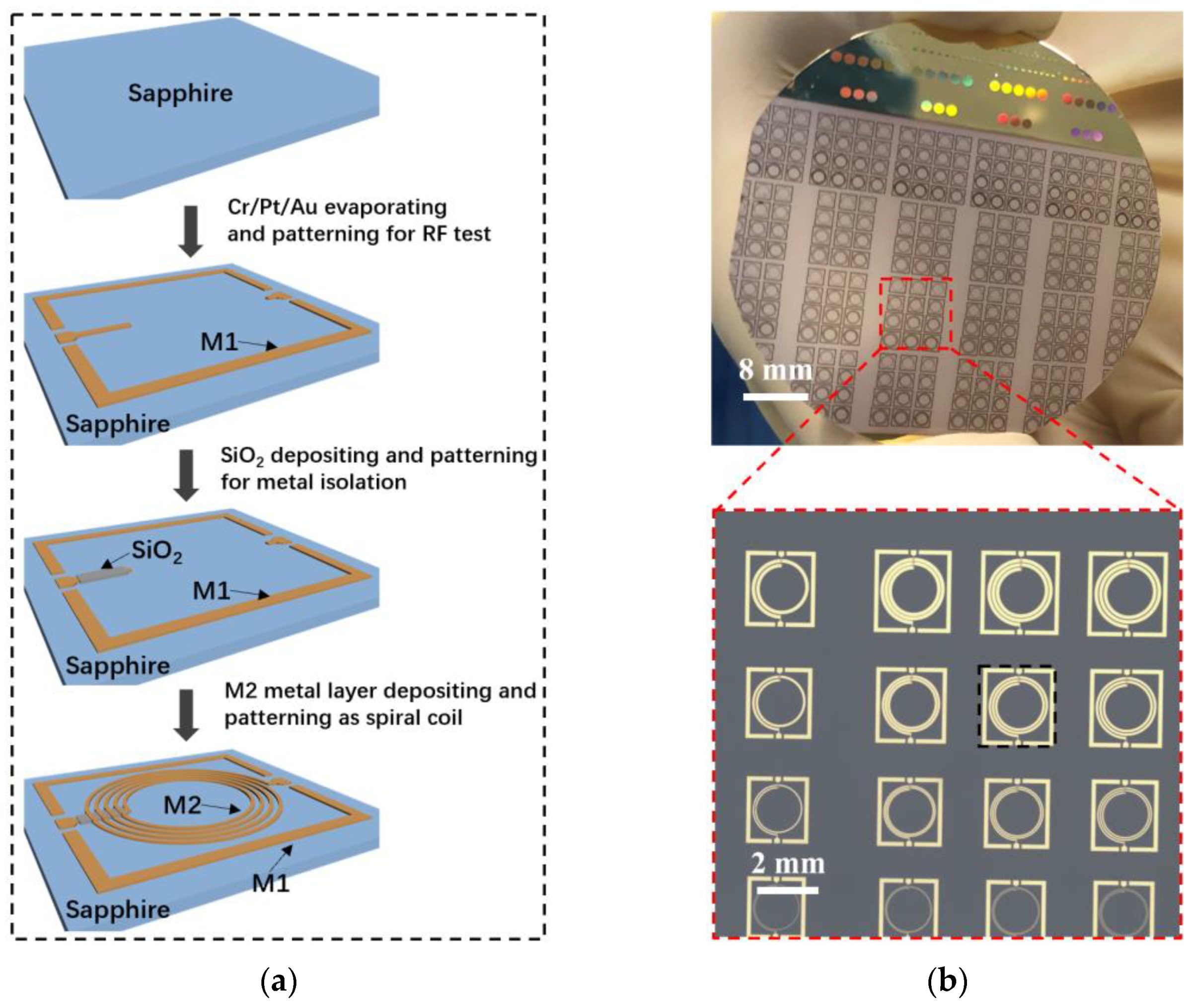
The fabrication process of the inductors is shown in
Figure 1a. The process started with cleaning the sapphire wafers in a 3:1 mixture of sulfuric acid (H
2SO
4) and hydrogen peroxide (H
2O
2), following with a deionized water cleaning. After that, ground-signal-ground (GSG) RF test patterns and underpass lead metal lines were fabricated by a combination of standard photolithography, metallization and lift-off processes. In this step, 70/40/200 nm Cr/Pt/Au (labeled as M1) was deposited by an E-beam evaporator. Then, a 600 nm SiO
2 insulation layer was deposited by plasma-enhanced chemical vapor deposition (PECVD), and the SiO
2 film off the underpass lead line was removed after photolithography and reactive ion etching (RIE). Finally, the second metal multilayer (labeled as M2) was fabricated as spiral coils.
For Cu-based spiral coils, a bilayer of Cr/Cu was sputtered initially. Sequentially, Ni/Au, Ti/Au or Cr layers were evaporated to protect the sidewalls of the underlying pattern [
15]. For Al-based spiral coils, Cr/Al/Ti/Au was evaporated in sequence.
Figure 1b shows the optical and microscope images of spiral inductors, respectively.
A series of inductors were fabricated with various layout parameters including number of turns (N), spiral metal line width (W), spacing between turns (S), inner radius (Rin), total thickness of metal multilayer (tme), and thickness of silicon dioxide insulation layer (tox). Analysis on these parameters lays a foundation for establishing corresponding model library and provides an insight into the design and optimization of the inductors on sapphire. If not specified below, the default design parameters are Rin = 600 μm, N = 4.5, tme = 2 μm, tox = 0.6 μm, W = 30 μm, and S = 10 μm.
Four-probe method was used to evaluate the electrical conductivities of the metal multilayers, which are 1 × 1 cm2 in size with a total thickness of 2 μm where Al or Cu layer were kept as 1.7 μm. A total of 12 samples (3 samples for each kind of the metal multilayer) were fabricated to check the consistency and repeatability of the measurement results. Pure 2 μm single-layer Al and Cu were also included as control groups in the experiment. The distance between two adjacent probes was fixed at 1 mm. The measurement results were imported into the material library of high frequency structure simulator (HFSS) to predict the characteristics of spiral inductors integrated on sapphire before fabrication process.
In addition, Auger electron spectroscopy (AES) combined in-situ ion sputtering (PHI 710, ULVAC-PHI, Inc., Chigasaki, Japan) was used to obtain the in-depth profiles of the multilayers. Diverse Ar+ ion bombardment energies were adopted to etch the sublayers with different thicknesses in order to obtain clear interfaces.
On-wafer
S-parameters measurements were carried out using an E5071C network analyzer with a Cascade Microtech M150 probe station, and the system was calibrated using the SOLT technique in the range of 300 MHz to 3 GHz. The apparent inductance (
L), apparent resistance (
R), and quality factor (
Q) [
16,
17,
18] were calculated using the following equations, where
Y11 was the two-port admittance matrix of the de-embedded coil.
Modified equivalent physical model and analytical formulas were constructed in Agilent Advanced Design System (ADS), in which iterative optimization for the elements was performed to extract equivalent parameter values. This process could be time-saving and flexible, benefitting from the frequency-independent elements.
3. Results and Discussions
Theoretically, multilayer metal has a higher sheet resistance than that of pure metal, according to the formula as follows [
19], which is used to estimate effective sheet resistance (
Rsheet):
where
n represents the
nth sublayer of the multilayer,
tn and
ρn are the thickness and resistivity of the
nth sublayer, respectively. This can be attributed to the multilayer acting as parallel resistors [
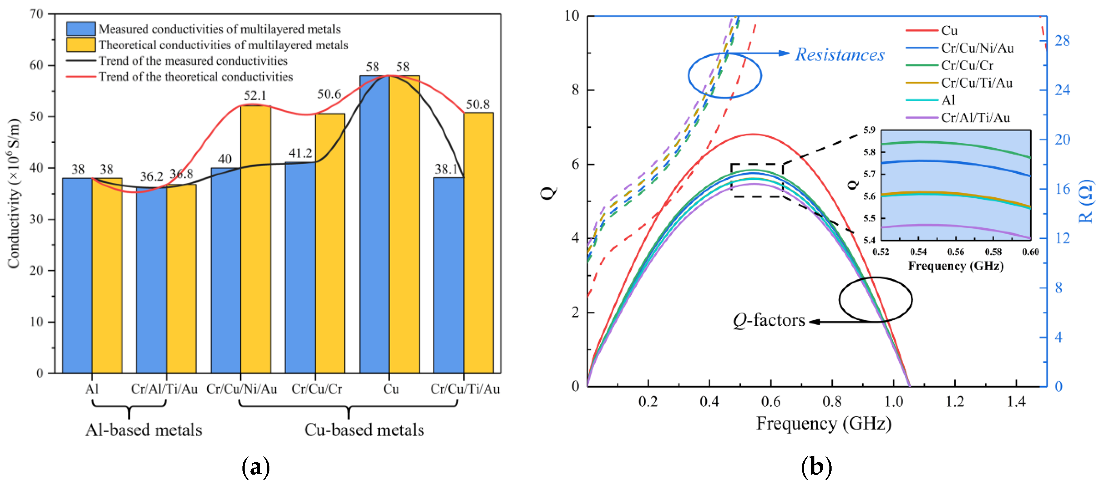
20]. Nevertheless, the theoretical conductivities of the multilayers approach those of the pure metals, for the contribution of the other sublayers is small as compared to that of the Cu or Al layer, which can be observed in
Figure 2a.
However, this was not the case for the samples in our measurement, with 23.2%, 18.6% and 24.8% reduction in conductivity for Cr/Cu/Ni/Au, Cr/Cu/Cr and Cr/Cu/Ti/Au, respectively, in comparison with the theoretical values. Oxidation of the metal and alloying formed by the interdiffusion between the sublayers account for the deterioration in their electrical properties. In contrast, a reduction of only 1.6% for Cr/Al/Ti/Au was observed. According to the four-probe measurement result, the order of the conductivity from the greatest to the least was σCr/Cu/Cr, σCr/Cu/Ni/Au, σCr/Cu/Ti/Au, and σCr/Al/Ti/Au. Overall, Al-based multilayer has a close electrical conductivity to that of Cu-based multilayers, with little performance deterioration as compared to the pure metal, although pure Cu exhibits the highest electrical conductivity of about 1.5 times that of pure Al.
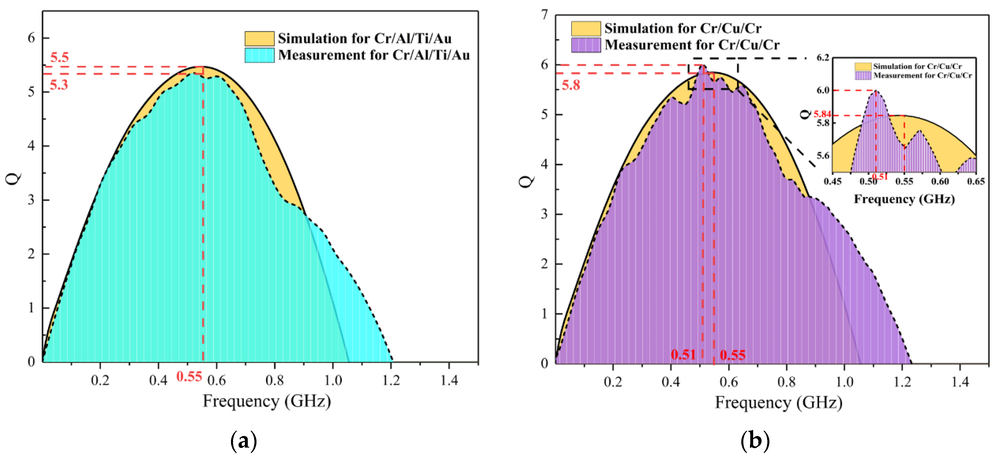
Figure 2b presents the simulation results of the
Q-factors and
R of the inductors as a function of frequency. The disparities in the performance between Al and Cu-based inductors are tiny. The
Q-factor reaches its maximum of 5.84 at 0.55 GHz for Cr/Cu/Cr, while the inductance mainly determined by the geometric parameters shows little susceptibility to different kinds of metallization systems.
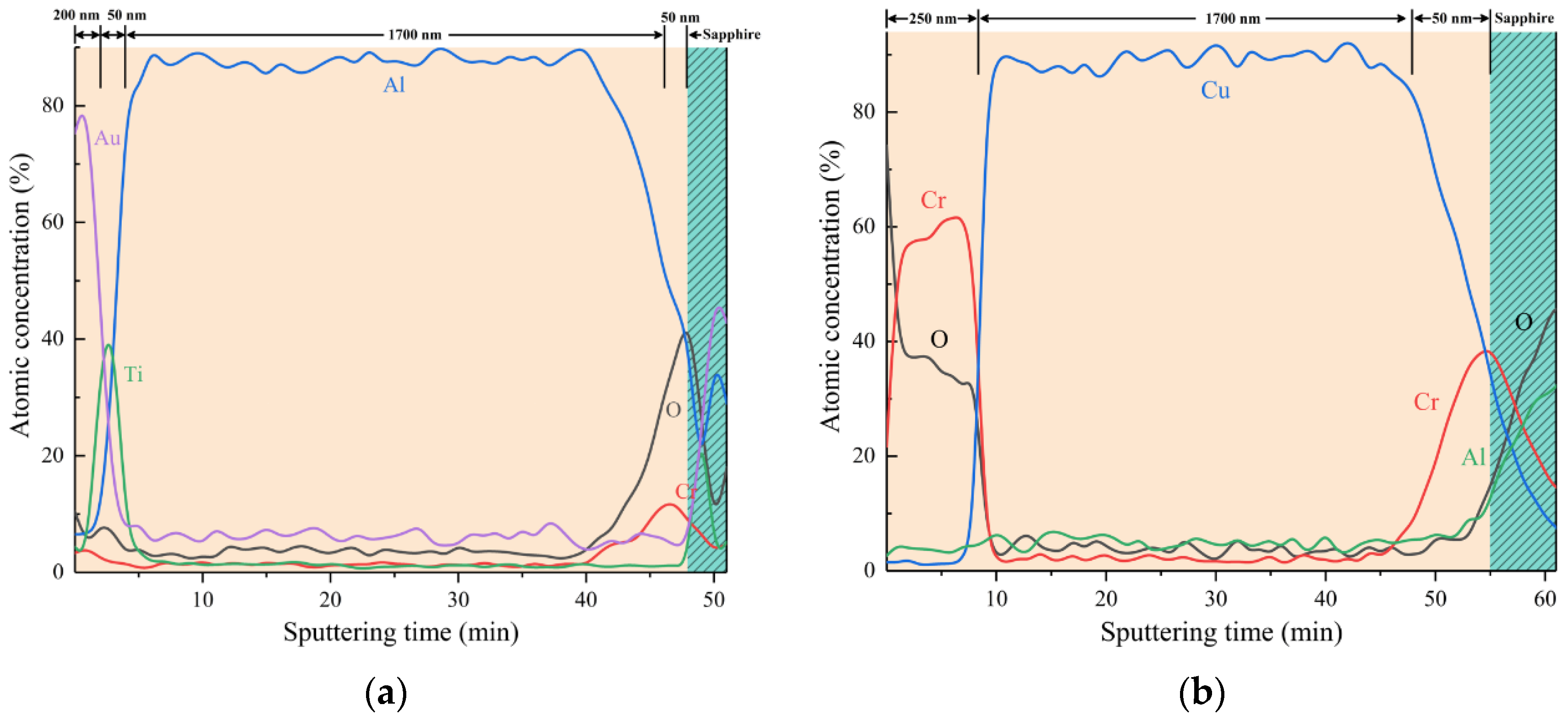
AES measurement was used to implement compositional and element analysis quantitatively, as displayed in
Figure 3. Sapphire substrate is indicated by the cyan-shaded regions, exhibiting high atomic concentrations of Al and O elements.
For Cr/Cu/Cr, chromium oxides on the surface exposed to the environment with low oxygen content were unsurprisingly detected (
Figure 3b), which served as protective layers for the pattern underneath at the cost of deteriorating electrical conductivity of the multilayer. A 250 nm top Cr layer was employed in order to keep consistent thickness of other sublayers in the four control samples. In Cr/Cu/Ni/Au, the binary phase of Ni with Cu spreading throughout the entire conductor layer can be seen in
Figure 3c, although 200 nm Ni was supposed to be an effective barrier layer. That is owing to the thermal energy facilitating the diffusion of Ni into Cu during the E-beam evaporation process.
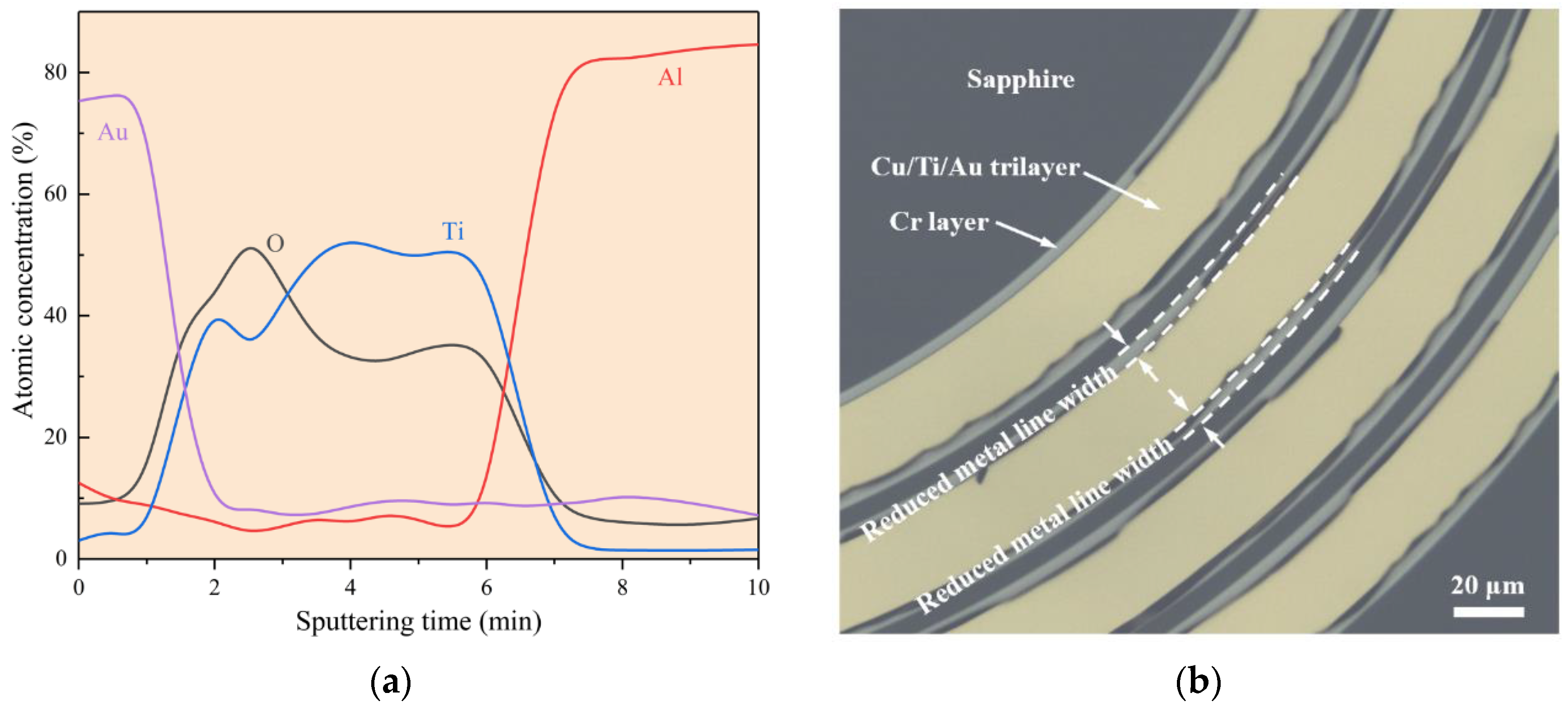
For Cr/Cu/Ti/Au, Ti barrier layer between Cu and Au was oxidized. This situation also happened for the sample with a thickened Au top layer of 200 nm, which denies the hypothesis that 50 nm Au is porous and too thin to be an effective protective layer whereby the Ti is directly exposed to the corrosive medium. It is found that oxidation of the Ti originates from the handover between sputtering and evaporation processes, during which oxygen inevitably adsorbed onto the surface of Cu. Excellent gettering properties of Ti require very low levels of residual water and oxygen. Another measurement performed on the Cr/Al/Ti/Au-2 sample confirmed our analysis, in which Cr/Al and Ti/Au bilayers were evaporated separately with a process of opening the chamber door for 2 min between them (three-step method in
Table 1), oxidation of the Ti also occurred as shown in
Figure 4a. Sputtering all metal sublayers sequentially in the vacuum chamber may solve this problem. Nonetheless, in the process of photoresist stripping and cleaning, the sidewalls of Cu layer are prone to be oxidized and flake off, thus metal line width reduces (
Figure 4b).
Among four kinds of samples, Cr/Al/Ti/Au had clear interfaces with less problems of the binary phase and the oxidation mentioned above, as the Al2O3 forming on the Al surface affords it a better corrosion resistance than Cu. Despite this, alloying between the adhesive layer and the conductor layer was observed in all samples.
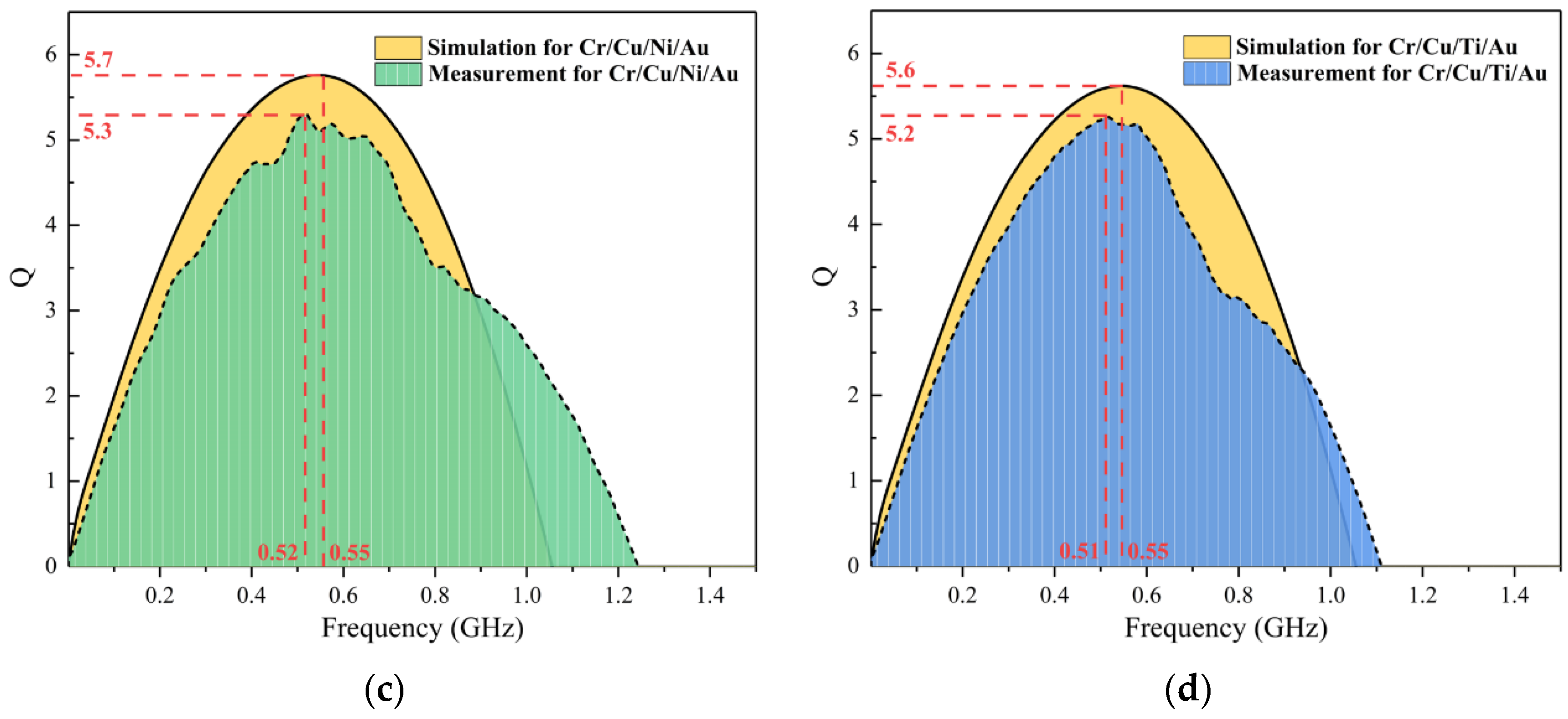
Measured
Q-factors for these four kinds of inductors are presented in
Figure 5a–d. Maximum value of
Q curve (
Qm), usually referred to as one of the bench marks to evaluate the quality of inductors, was around 0.55 GHz for all inductors.
Qm was 6 for Cr/Cu/Cr whereas the smallest one was 5.2 for Cr/Cu/Ti/Au,
Qm of the Cr/Al/Ti/Au inductor was 5.6. The Al-based metal multilayer shows competitive ability in fabricating actual inductor on sapphire, as compared to Cu-based multilayers whose electrical conductivities degrade due to the oxidation or interdiffusion of the metals. Additionally, simulation results match well with the measured ones in spite of slight variations in
Qm and resonant frequencies that exist between them.
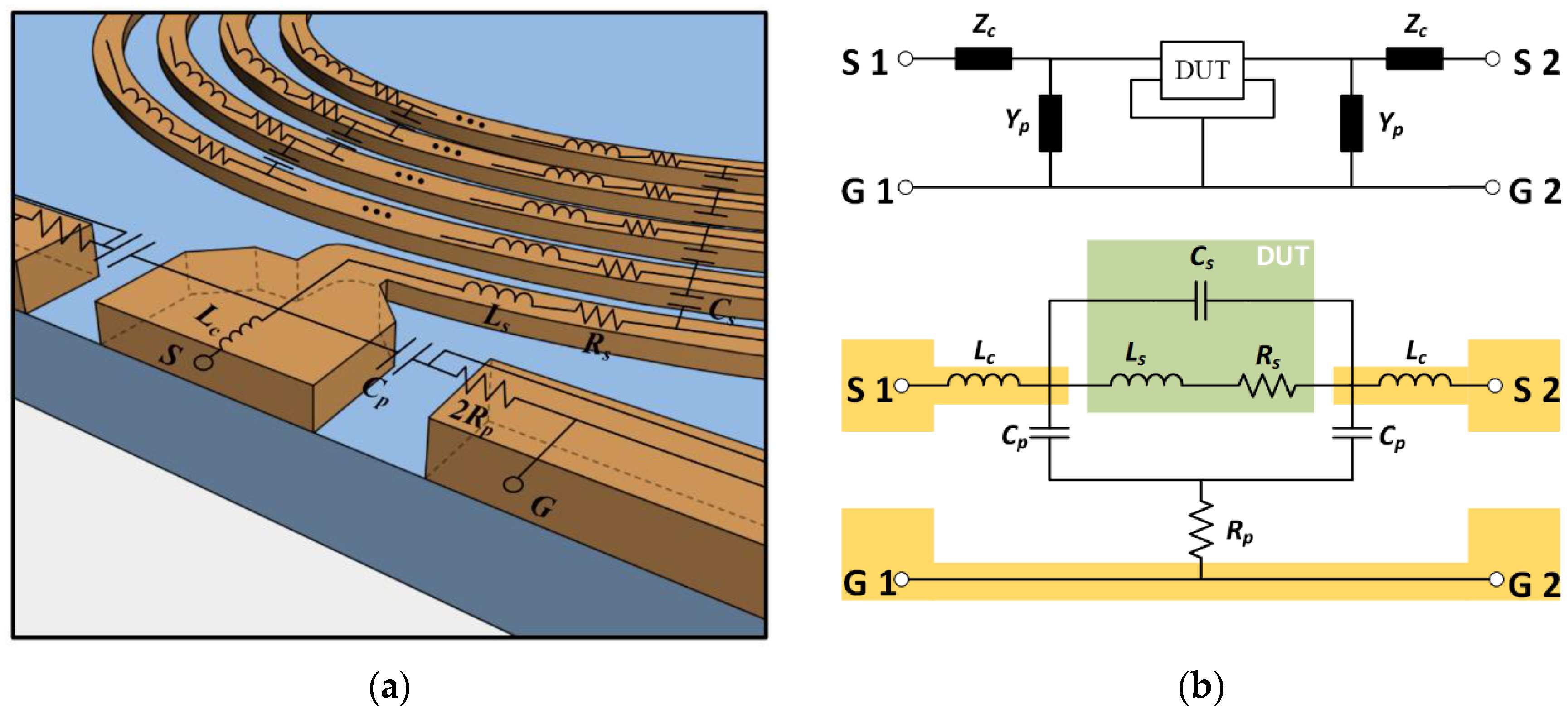
Conventionally, three-element model ruling out the substrate-related elements on the basis of Pi model [
16,
21] is often used for on-chip spiral inductors on sapphire (DUT in
Figure 6b), in which
Ls and
Rs represent the series inductance and resistance, and capacitance
Cs models the feed-through path between the spiral and the underpass metal line. In addition, the parasitic effect from GSG test pattern, which is used to be de-embedded relying on “open”, “through” and “short” structures, was included into our model. Shunt admittances
Yp from the contact pads and the interconnects were modeled by capacitance
Cp and resistance
Rp [
22,
23], while contact impedances
Zc between the probes and the pads at input and output ports were indicated by series
Lc [
24,
25], it cannot be ignored for its great influence on high frequency characteristic of the model. Except
Rs, the other elements are frequency-independent.
Analytical formulas [
21] considering skin effect in the conductor are used to evaluate
Rs as follows:
where
δ is the skin depth,
ρ,
μ, and
f represent the resistivity, permeability and frequency, respectively.
where
teff is defined as metal effective thickness,
l and
w represent the metal line length and width, respectively. A correction factor
k is introduced in Equation (7). In our experiment, empirical value for
k ranges from 0.6 to 0.7 depending on how well the model data fits with the experimental result.
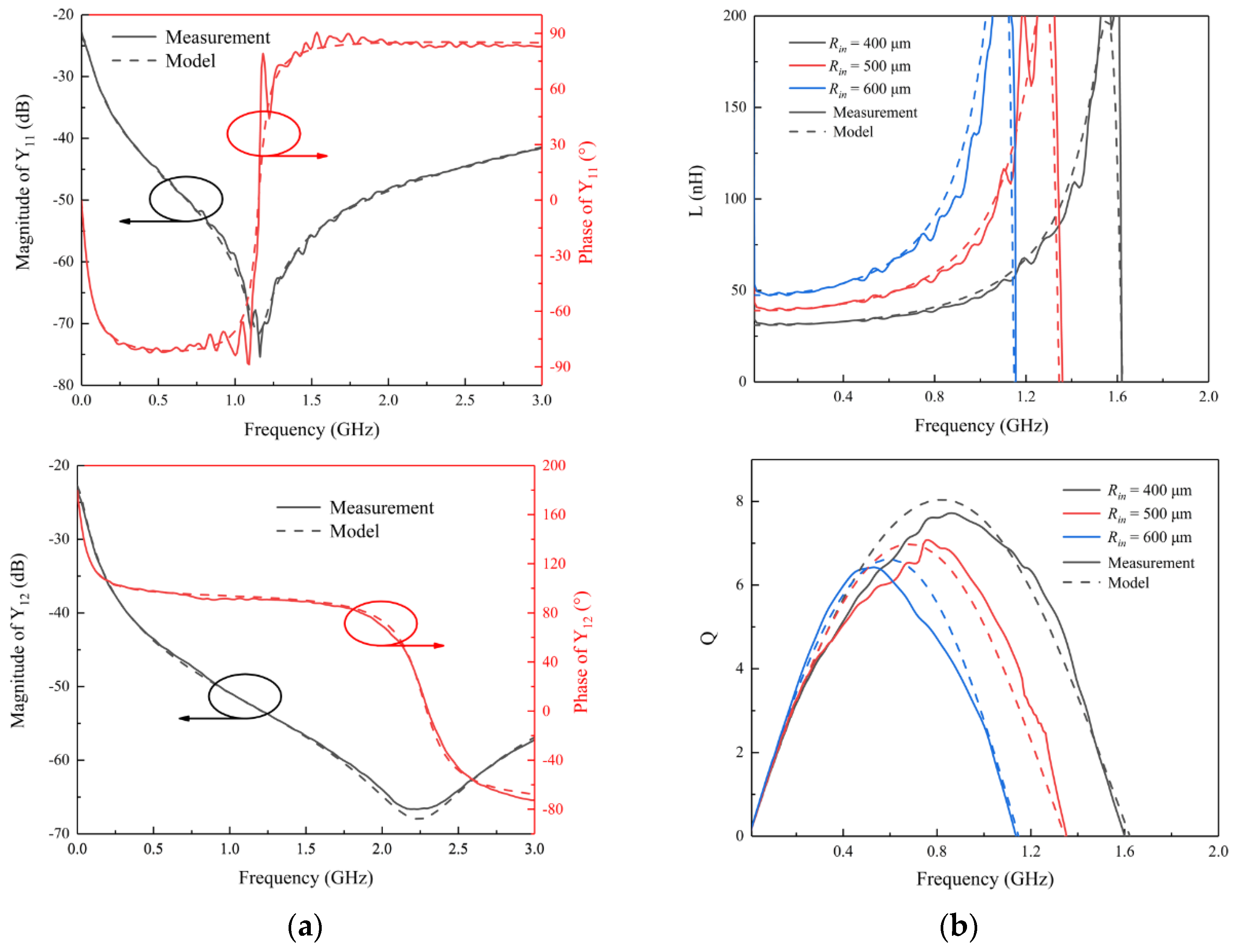
Figure 7 shows measured and modeled
Y-parameters,
L values and
Q-factors for the inductors, respectively. Good agreement between them verifies the validity of our model and extraction scheme. By fitting with the embedded measurement result, series and parasitic parameters can be extracted rapidly. They are listed in
Table 2. Analysis on these parasitic parameters originating from contact pads and interconnections provides an insight into RF measurement.
