Article

Solution-Processed NiO as a Hole Injection Layer for Stable Quantum Dot Light-Emitting Diodes

Department of Advanced Materials Engineering, Kyonggi University, Suwon 16227, Korea
*
Author to whom correspondence should be addressed.
Appl. Sci. 2021, 11(10), 4422; https://doi.org/10.3390/app11104422
Submission received: 5 March 2021 / Revised: 3 May 2021 / Accepted: 9 May 2021 / Published: 13 May 2021

Abstract

:
In this work, we fabricated quantum dot light-emitting diodes using solution-processed NiO as the hole injection layer to replace the commonly used poly(3,4-ethylenedioxythiophene): poly(styrene-sulfonate) (PEDOT:PSS) layer. We successfully prepared NiO films by spin coating the NiO precursor, then annealing them, and then treating them with UV-ozone under optimized conditions. The best device with the NiO film shows higher current efficiency (25.1 cd/A) than that with the PEDOT:PSS layer (22.3 cd/A). Moreover, the long-term stability of the devices with NiO which is annealed at 500 °C is improved substantially. These results suggest that the NiO layer can be a good alternative for developing stable devices.

1. Introduction

Colloidal quantum dots (QDs) are unique semiconductor nanomaterials with emission colors that can be tuned by controlling their size [1,2,3]. Furthermore, their organic ligands render them solution-processable, leading to cost-effective processing. Since Colvin et al. demonstrated the first quantum dot light-emitting diodes (QLEDs) using QDs as the emitting layer (EML) [4], the performance of QLEDs has improved rapidly by taking advantage of the narrow emission lines and excellent luminescence characteristics of the QDs. In 2019, Shen et al. demonstrated high-performance QLEDs that emit three primary colors; they reported maximum external quantum efficiencies of 21.6, 22.9, and 8.05% for red, green, and blue-emitting QLEDs, respectively [5]. However, due to the restriction of hazardous substances compliance in Europe, the substitution of Cd-based QDs with eco-friendly materials has become an important task for electroluminescence (EL) devices Therefore, several options such as indium phosphide and Cu-In-S based QDs have been studied recently [6,7]. Additionally, in the sequential formation of various thin films of EL devices, solution processes lead to less stable films than in the high-vacuum processes owing to the inevitable influence of the organic solvents used in the solution process on the underlying layers.
QLEDs with a standard structure have a large hole injection barrier between the indium tin oxide (ITO) electrode and hole transport layer (HTL). Therefore, poly(3,4-ethylenedioxythiophene): poly(styrene-sulfonate) (PEDOT:PSS) is widely used as a hole injection layer (HIL) for efficient hole transport to the EML. However, PEDOT:PSS, which is hygroscopic as well as acidic, can erode the ITO layer, thus severely decreasing the device’s stability and limiting its practical application. [8] Therefore, it is necessary to develop inorganic materials with better chemical stability as alternatives for PEDOT:PSS to improve the efficiency and stability of QLEDs. As such, various metal oxides such as CuO, MoOx and V2O5 have been investigated as HILs in QLEDs [9,10,11]. However, the performance of the reported QLEDs based on various p-type inorganic layers is still not comparable to those of the QLEDs with PEDOT:PSS because of the poor hole injection in the former case. In this study, nickel oxide (NiO) was chosen as an alternative inorganic material for the HIL. Since NiO is a wide band gap (3.6~4.0 eV) p-type semiconductor with a conductivity of 10−13 S/cm, it has shown significant promise as a hole-injecting and electron-blocking material. [12,13] In this study, we successfully synthesized an NiO precursor (Ni(CH3COO)2·4H2O) using a sol–gel method under ambient conditions. For the formation of the NiO film, we used the spin-coating method followed by the annealing of the deposited film and UV-ozone treatment. Further, we studied various optical and structural properties of the NiO films to confirm the formation of a stable HIL. The resulting QLEDs showed the maximum current efficiency and luminance of 25.1 cd/A and 34,125 cd/m2, respectively, indicating that NiO can be a promising alternative to inorganic material for the HIL of QLEDs.

2. Experiment

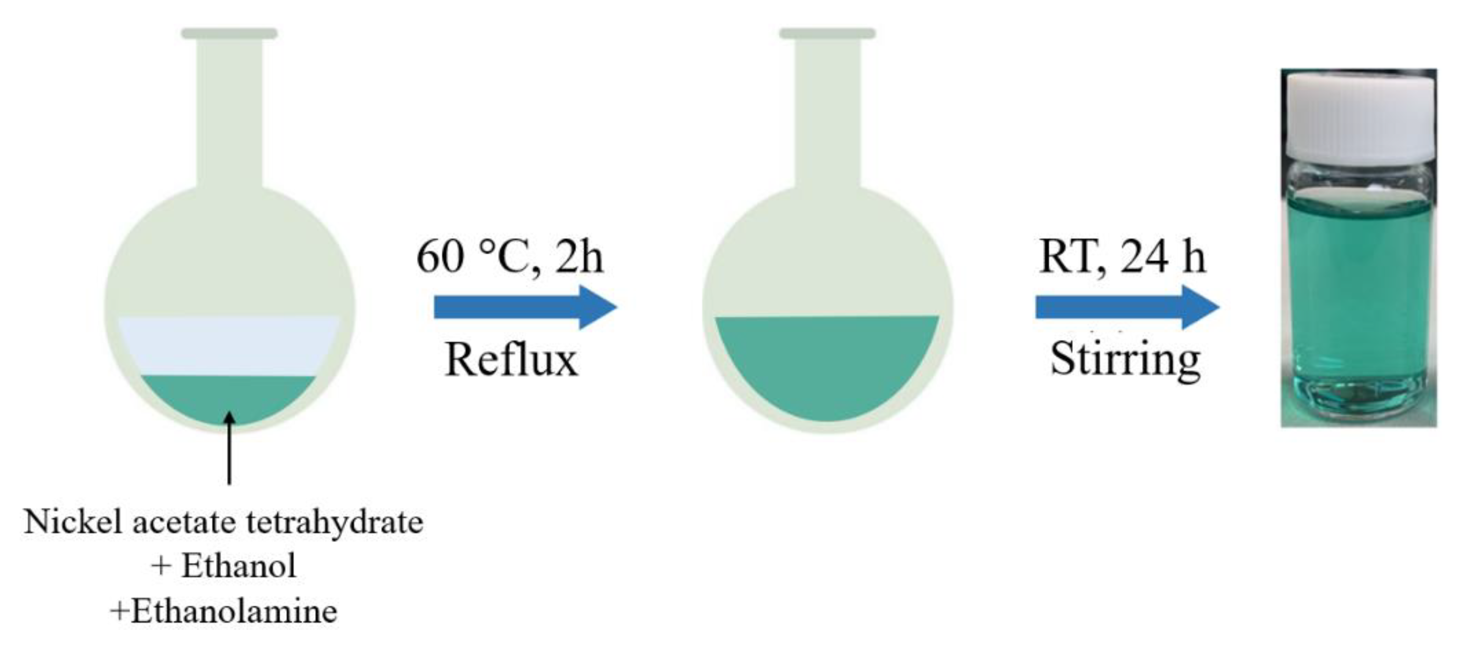
2.1. Synthesis of NiO Precursor

The NiO precursor was synthesized according to a previously reported method [14]. As shown in Figure 1, a solution of the NiO precursor was prepared by dissolving nickel acetate tetrahydrate (Ni(CH3COO)2·4H2O) and ethanolamine (NH2CH2CH2OH) in ethanol at a molar ratio of 1:1. The precursor solution was first stirred at 60 °C for 2 h and then at room temperature for 24 h. Finally, the solution was filtered through a 0.45 μm polytetrafluoroethylene (PTFE) filter to remove impurities before use.

2.2. Synthesis of Green QDs

In the synthesis of green QDs, CdZnSeS core QDs with the composition-gradient composition were first prepared as follows: 0.14 mmol of CdO, 3.41 mmol of ZnO, and 7 mL of oleic acid (OA) in a three-neck flask were degassed and heated to 150 °C with N2 flowing, followed by the addition of 15 mL of 1-octadecene (ODE) and subsequent heating to 310 °C. Next, an anionic stock solution, which was prepared by dissolving 1.76 mmol of Se and 2.64 mmol of S in 2.2 mL of trioctylphosphine (TOP), was rapidly injected to the above mixture and the core reaction was maintained at that temperature for 10 min. Subsequently, 1.6 mmol of S dissolved in 2.4 mL of ODE was introduced into the CdZnSeS QD growth solution and the reaction was observed for 12 min. After that, a Zn stock solution containing 2.86 mmol of Zn acetate dihydrate which was dissolved in 1 mL of ODE and 4 mL of OA, was quickly injected and subsequently an S stock solution, containing 9.63 mmol of S dissolved in 5 mL of TOP, was introduced dropwise. After that, this ZnS shelling was performed at 270 °C for 20 min. As-synthesized green CdZnSeS/ZnS QDs were subjected to repeated rounds of purification by centrifugation. The resulting purified QDs were filtered through a 0.20 μm PTFE filter and dispersed in hexane for spin-coating EML.

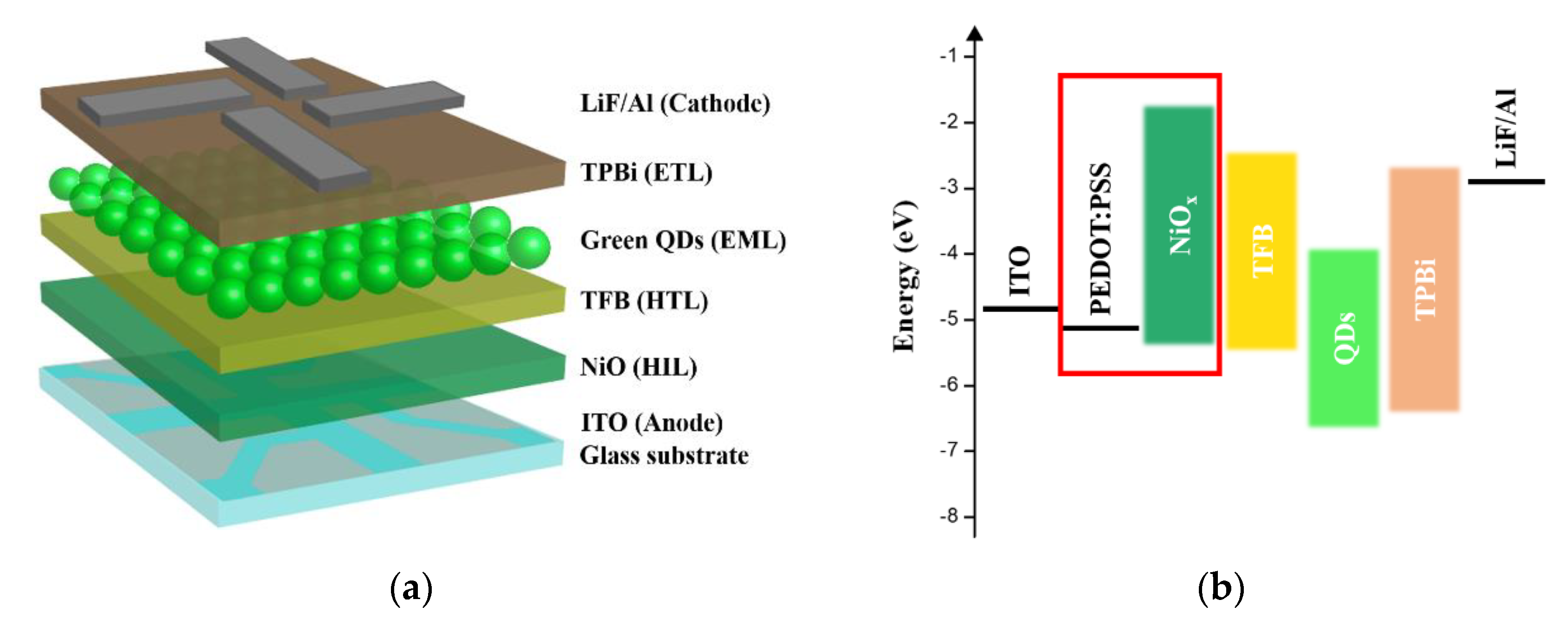
2.3. Fabrication of QLEDs

For device fabrication, the ITO-coated glass substrates were first cleaned by ultrasonication with isopropyl alcohol and deionized water. Before the deposition of the HIL, the substrates were cleaned with a UV-ozone treatment for 15 min to generate a hydrophilic surface. Subsequently, the NiO precursor was spin-coated as the HIL on the substrate at 2500 rpm for 60 s and then annealed in air at different temperatures (300–500 °C). After the annealing step, the NiO films (15 nm) were treated with UV-ozone for 10 min. For comparison, reference devices with PEDOT:PSS HILs were also prepared. Next, the coated substrates were transferred to an N2-filled glove box for spin-coating the poly[(9,9-dioctylfluorenyl-2,7-diyl)-co-(4,4′-(N-(4-sec-butylphenyl)diphenylamine)] (TFB) and QD layers. The TFB layer was spin-coated at 2000 rpm for 35 s using an 8 mg/mL solution in chlorobenzene, and then baked at 150 °C for 30 min. Thereafter, a suspension of CdZnSeS/ZnS QDs in hexane (10 mg/mL) was spin-coated at 2000 rpm for 20 s. To deposit the electron transport layer (ETL) and the cathode, the substrates were transferred into a thermal evaporator and TPBi (40 nm), LiF (1 nm), and Al (100 nm) layers were thermally deposited sequentially under a base pressure of 5 × 10⁻⁶ Pa. Finally, the devices were encapsulated in glass using an ultraviolet sealant.

2.4. Characterization

X-ray diffraction (XRD) of the synthesized NiO was conducted using a MiniFlex II X-ray diffractometer (Rigaku, Tokyo, Japan). The transmittance of the NiO films was evaluated using an OPTIZEN POP UV-visible spectrophotometer (KLAB, Daejeon, Korea). Both the EL spectra and the current density–voltage–luminance (J–V–L) characteristics of the QLEDs were evaluated using a CS2000 spectroradiometer (Minolta, Tokyo, Japan) under ambient conditions. The thickness and surface profiles of the NiO layers were obtained using an F20-UV thickness measurement system (Filmetrics, San Diego, CA, USA) and an atomic force microscopy (AFM, PSIA XE-100, Suwon, Korea), respectively. The electronic structures of NiO were investigated using an ESCALAB 250 ultraviolet photoelectron spectroscopy (Thermo Scientific, Waltham, MA, USA).

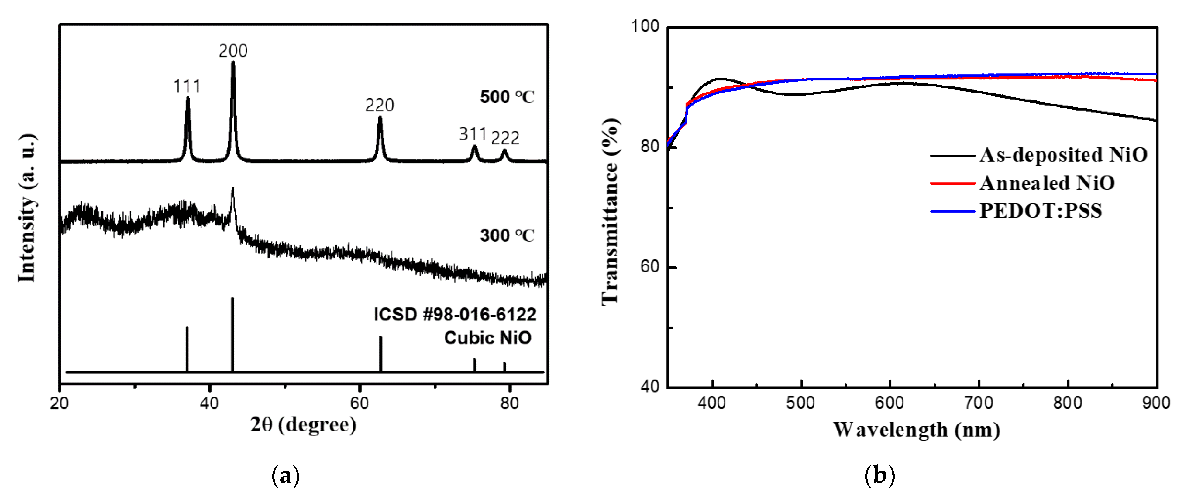
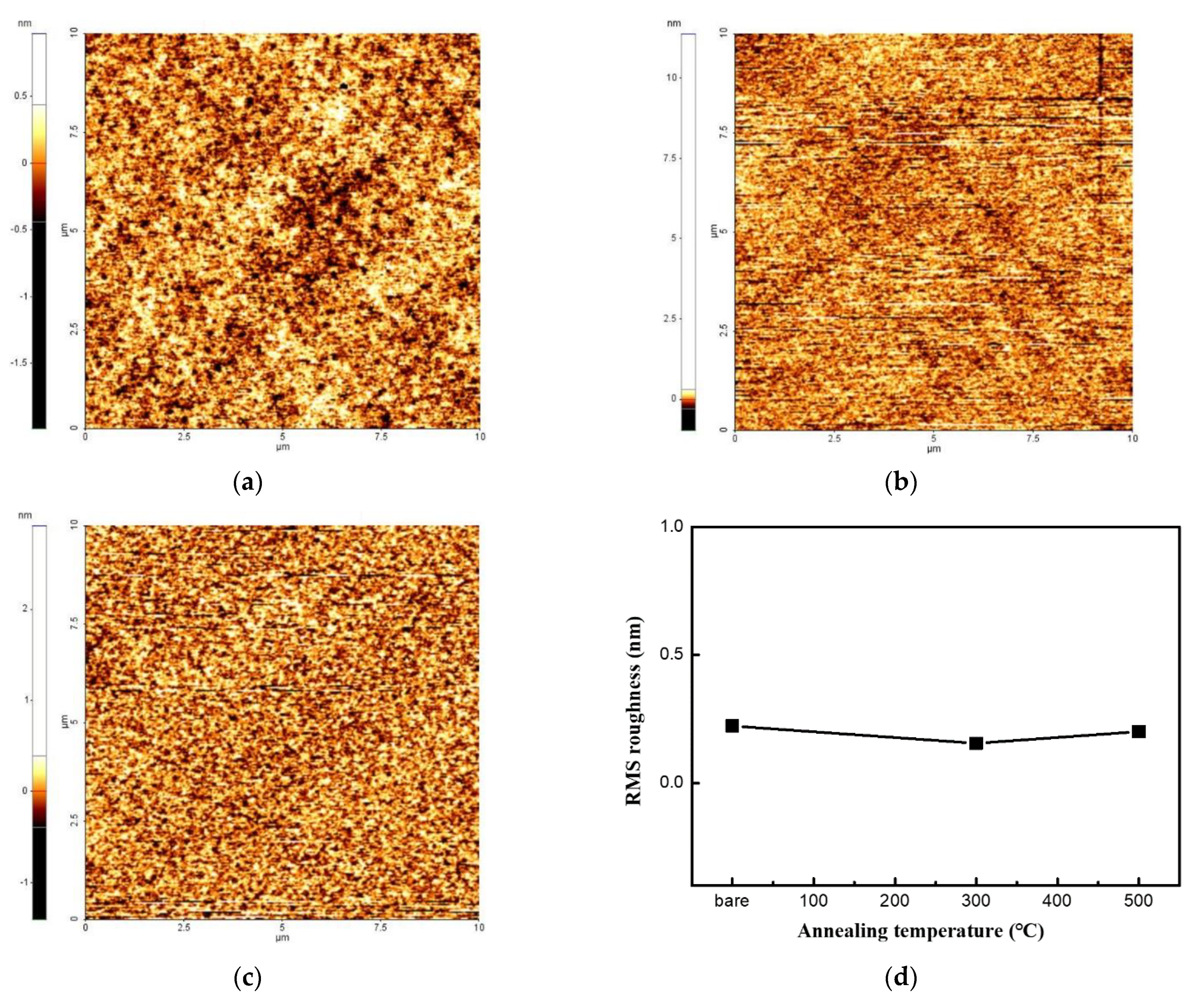
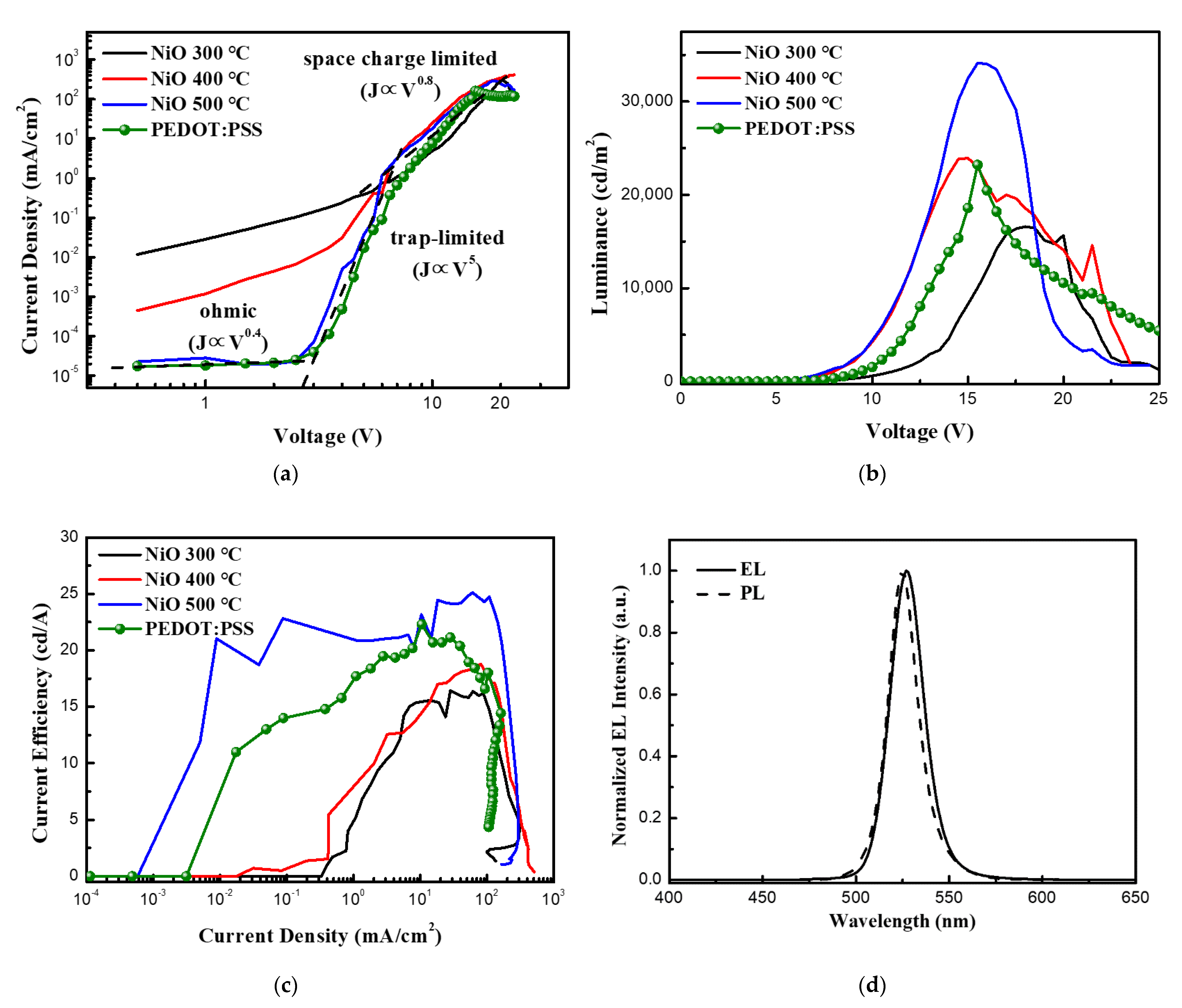
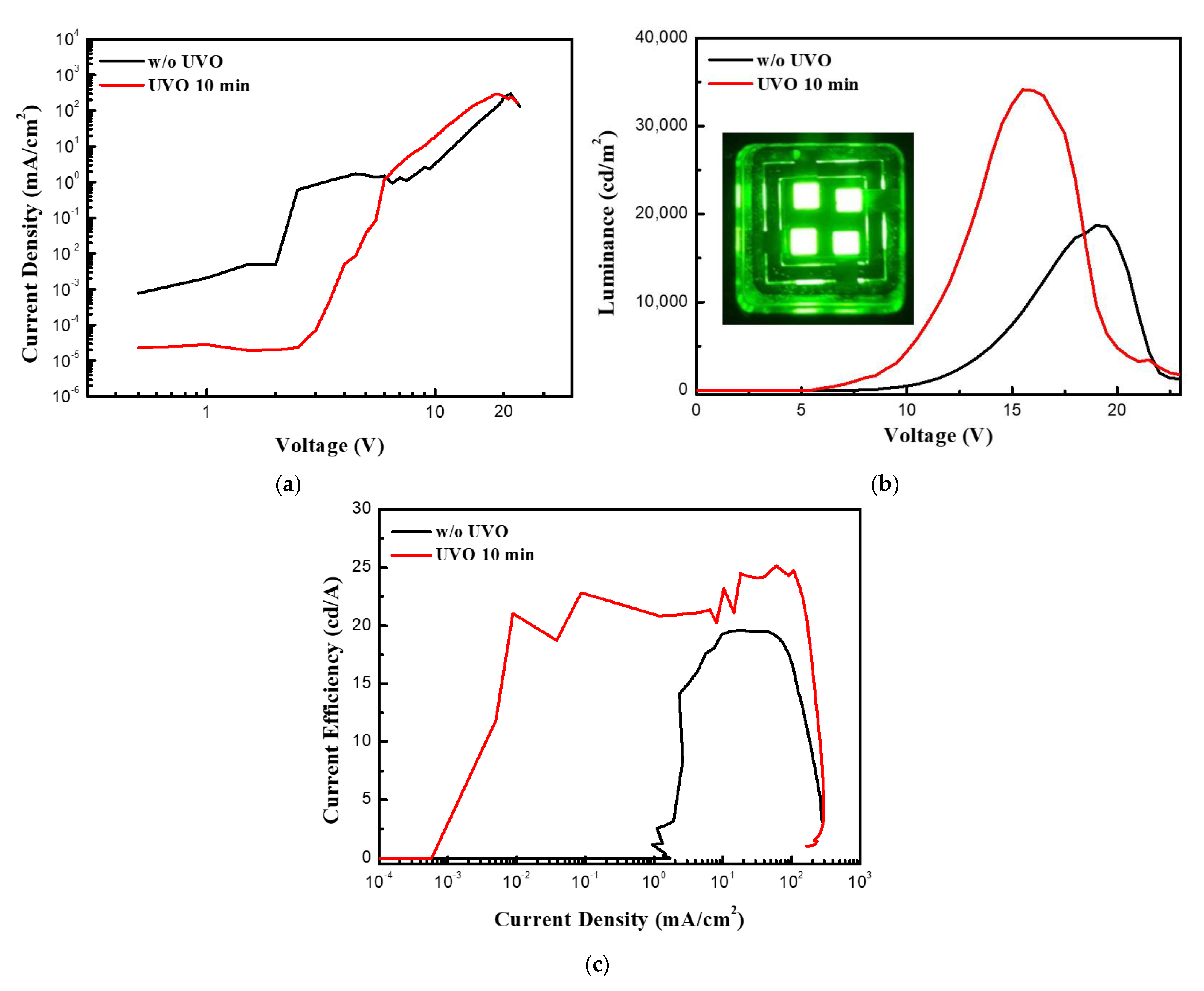
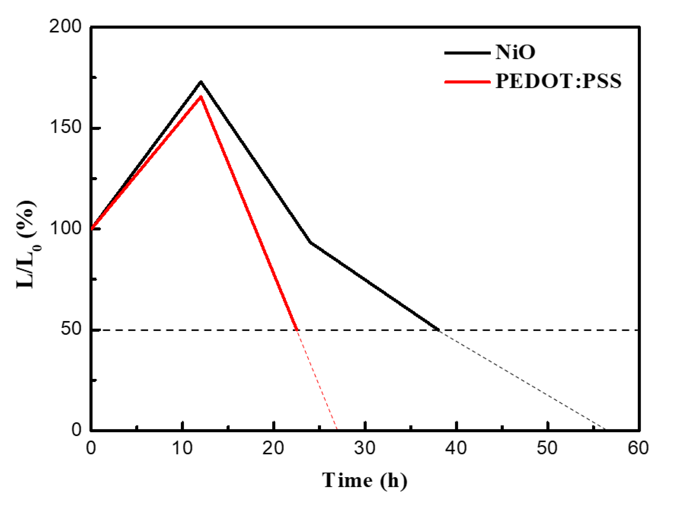
3. Results and Discussion

Figure 2a presents the XRD pattern of the annealed NiO films that crystallized in the face-centered cubic phase without the formation of any new phase. In detail, the XRD pattern presents peaks at 2θ = 37.20°, 43.20°, 62.87°, 75.20° and 79.38° corresponding to the (111), (200), (220), (311), and (222) crystal planes of the NiO, respectively. The optical transmittance data for the NiO layer, which annealed at 500 °C (Figure 2b), show a high transmittance of more than 90% in the entire visible region and no difference from those of the PEDOT:PSS layer. This transmittance value is either similar to or higher than the alternative inorganic materials for HIL [11,15]. As shown in Figure 2a, the transmittance of films annealed at elevated temperatures increases because of the improved crystalline microstructure [16]. Because the materials under the EML inevitably absorb light emitted from the QDs in the bottom emission structure, the transmittance must be ensured before the fabrication of the devices.
Figure 3a illustrates a schematic of the device structure of a standard QLED with NiO as the HIL. It consists of ITO (anode)/NiO (HIL)/TFB (HTL)/green QDs (EML)/TPBi (ETL)/LiF/Al (cathode). According to the energy level diagram in Figure 3b [17,18,19], PEDOT:PSS and NiO have similar work functions (Table S1 in the Supplementary Materials). However, NiO not only has a great hole injection ability, but also an electron-blocking function because of its deep valence band and wide bandgap. Owing to the high energy level of its conduction band minimum, the NiO can block further transport of electrons to the anode, while its well-matched valence band maximum allows holes to move efficiently to the EML.
Figure 4 shows the AFM images of solution-processed NiO thin films annealed at different temperatures. The charge transport layers formed by the solution process often show a rough surface or pinholes, which leads to poor performance or severe electrical leakage of devices. The AFM images confirm the formation of ultra-smooth surfaces of the NiO thin films with a root mean square (RMS) roughness of less than 0.3 nm, indicating that all the NiO films are smoother than the ITO film on glass [20]. These results indicate that the NiO layer effectively covers the ITO surface, and the annealing temperature hardly affects the morphology of the NiO film.
Figure 5 presents the optoelectronic properties of the QLEDs with the NiO films annealed at different temperatures. Improvements in both the electrical properties and the luminance were achieved with an increase in the annealing temperature. It is well known that three different conduction regimes (ohmic, trap-limited, and space charge limited conduction) are apparent in the QLEDs, and different power-law relationships in each region are shown in Figure 5a [21]. The leakage current in the Ohmic region decreased significantly, and the current density above the turn-on voltage improved after the annealing process. The device with the NiO annealed at 500 °C clearly showed trap-limited behavior above the turn-on voltage, and then changed to space-charge limited conduction as the operating voltage was increased. Interestingly, the electrical properties of the devices annealed at 500 °C were found to be almost identical to those of the devices with PEDOT:PSS. To further investigate the hole injection into the EML, hole-only devices (HODs) were fabricated using NiO layers annealed at 500 °C, and their current densities were compared with those of HODs with PEDOT:PSS (Figure S1 in the Supplementary Materials). The HODs consisted of ITO/NiO or PEDOT:PSS/TFB/QDs/MoO3/Al layers. The current density of the HODs with an NiO layer annealed at 500 °C is comparable to that of the HODs with PEDOT:PSS. For the device with an NiO annealed at 500 °C, the peak luminance of 34,125 cd/m2 was achieved at 15.5 V (corresponding to a current density of 164.5 mA/cm2), and a current efficiency of 25.1 cd/A was obtained at a current density of 60.4 mA/cm2. The higher the annealing temperature applied to the NiO layer, the higher the conductivity obtained (Figure S2 in the Supplementary Materials), which solves the charge imbalance in the EML due to the slow hole transport. As shown in Figure 5d, there is no big difference in the shape and peak position of the EL peak and the PL peak.
Further, QLEDs based on NiO layers annealed at 500 °C were fabricated either with UV-ozone treatment or without it, and their optoelectronic properties were investigated (Figure 6). In the absence of a UV-ozone treatment, the electrical properties were unstable, and a high leakage current was observed in the Ohmic region. By contrast, after 10 min UV-ozone treatment of the NiO layer, the current density, luminance, and current efficiency increased significantly. Sun et al. reported that the UV-ozone treatment was an effective technique to improve the performance of QLEDs [22]. The enhanced hole injection with the NiO layer after the UV-ozone treatment led to improved optoelectronic properties, as shown in Figure 6.
The application of inorganic HILs can thus provide many advantages, especially improved device stability. Figure 7 shows that the half-life of QLEDs with NiO layers was 2.3 times longer than that of QLEDs with PEDOT:PSS. As shown in Figure S1, the electrical characteristics of two HODs (NiO or PEDOT:PSS) were very similar to each other. Therefore, the device stability mainly depends on the used material itself. Additionally, UV-ozone treated QLEDs with NiO layers annealed at 500 °C exhibited long shelf lives; moreover, they showed stable EL emission even after 2 weeks. This result suggests that our QLEDs with inorganic HILs have better resistance to oxygen and humidity than traditional QLEDs do.

4. Conclusions

In summary, NiO was successfully synthesized using a sol–gel method, and its applications were investigated as an alternative HIL for QLEDs at different annealing temperatures. The NiO layer annealed at 500 °C showed high crystallinity, good transparency, and ultra-smooth morphology. With additional UV-ozone treatment, the QLEDs with the optimized NiO layer exhibited a peak luminance of 34,125 cd/m2 and current efficiency of 25.1 cd/A, which are higher than those of devices with PEDOT:PSS HILs. These promising results can lead to the development of highly stable all-inorganic QLEDs in the future.

Supplementary Materials

The following are available online at https://www.mdpi.com/article/10.3390/app11104422/s1, Table S1. Energy levels of NiO layer. Figure S1: Current density–voltage characteristics of hole-only devices using NiO or PEDOT:PSS. Figure S2: Current–voltage characteristics of NiO films annealed at various temperatures.

Author Contributions

Investigation, S.L.; writing—original draft preparation, S.L.; writing—review and editing, Y.K. and J.K.; supervision, J.K.; funding acquisition, J.K. All authors have read and agreed to the published version of the manuscript.

Funding

This research was financially supported by the ITECH R&D program of MOTIE/KEIT (project No. 20004978). This work was also supported by Kyonggi University’s Graduate Assistantship 2021.

Institutional Review Board Statement

Not applicable.

Informed Consent Statement

Not applicable.

Conflicts of Interest

The authors declare no conflict of interest.

References

  1. Shirasaki, Y.; Supran, G.J.; Bawendi, M.G.; Bulović, V. Emergence of colloidal quantum-dot light-emitting technologies. Nat. Photonics 2013, 7, 13–23. [Google Scholar] [CrossRef]
  2. Caruge, J.M.; Halpert, J.E.; Wood, V.; Bulović, V.; Bawendi, M.G. Colloidal quantum-dot light-emitting diodes with metal-oxide charge transport layers. Nat. Photonics 2008, 2, 247–250. [Google Scholar] [CrossRef]
  3. Zhang, H.; Su, Q.; Chen, S. Recent progress in the device architecture of white quantum-dot light-emitting diodes. J. Inf. Disp. 2019, 20, 169–180. [Google Scholar] [CrossRef] [Green Version]
  4. Colvin, V.L.; Schlamp, M.C.; Alivisatos, A.P. Light-emitting diodes made from cadmium selenide nanocrystals and a semiconducting polymer. Nature 1994, 370, 354–357. [Google Scholar] [CrossRef]
  5. Shen, H.; Gao, Q.; Zhang, Y.; Lin, Y.; Lin, Q.; Li, Z.; Chen, L.; Zeng, Z.; Li, X.; Jia, Y.; et al. Visible quantum dot light-emitting diodes with simultaneous high brightness and efficiency. Nat. Photonics 2019, 13, 192–197. [Google Scholar] [CrossRef]
  6. Saatsakis, G.; Michail, C.; Fountzoula, C.; Kalyvas, N.; Bakas, A.; Ninos, K.; Fountos, G.; Sianoudis, I.; Kandarakis, I.; Panayiotakis, G.S.; et al. Fabrication and Luminescent Properties of Zn–Cu–In–S/ZnS Quantum Dot Films under UV Excitation. Appl. Sci. 2019, 9, 2367. [Google Scholar] [CrossRef] [Green Version]
  7. Won, Y.H.; Cho, O.; Kim, T.; Chung, D.Y.; Kim, T.; Chung, H.; Jang, H.; Lee, J.; Kim, D.; Jang, E. Highly efficient and stable InP/ZnSe/ZnS quantum dot light-emitting diodes. Nature 2019, 575, 634–638. [Google Scholar] [CrossRef]
  8. Cao, F.; Wang, H.; Shen, P.; Li, X.; Zheng, Y.; Shang, Y.; Zhang, J.; Ning, Z.; Yang, X. High-efficiency and stable quantum dot light-emitting diodes enabled by a solution-processed metal-doped nickel oxide hole injection interfacial layer. Adv. Funct. Mater. 2017, 27, 1704278. [Google Scholar] [CrossRef]
  9. Ding, T.; Yang, X.; Bai, L.; Zhao, Y.; Fong, K.E.; Wang, N.; Demir, H.V.; Sun, X.W. Colloidal quantum-dot LEDs with a solution-processed copper oxide (CuO) hole injection layer. Org. Electron. 2015, 26, 245–250. [Google Scholar] [CrossRef]
  10. Vu, H.T.; Su, Y.K.; Chiang, R.K.; Huang, C.Y.; Chen, C.J.; Yu, H.C. Solution-processable MoOx for efficient light-emitting diodes based on giant quantum dots. IEEE Photon. Technol. Lett. 2016, 28, 2156–2159. [Google Scholar] [CrossRef]
  11. Zhang, H.; Wang, S.; Sun, X.; Chen, S. Solution-processed vanadium oxide as an efficient hole injection layer for quantum-dot light-emitting diodes. J. Mater. Chem. C 2017, 5, 817–823. [Google Scholar] [CrossRef]
  12. Wang, J.; Yang, P.; Wei, X.; Zhou, Z. Preparation of NiO two-dimensional grainy films and their high performance gas sensors for ammonia detection. Nanoscale Res. Lett. 2015, 10, 119. [Google Scholar] [CrossRef] [PubMed] [Green Version]
  13. Betancur, R.; Maymó, M.; Elias, X.; Vuong, L.T.; Martorell, J. Sputtered NiO as electron blocking layer in P3HT:PCBM solar cells fabricated in ambient air. Sol. Energy Mater. Sol. Cells 2011, 95, 735–739. [Google Scholar] [CrossRef]
  14. Manders, J.R.; Tsang, S.W.; Hartel, M.J.; Lai, T.H.; Chen, S.; Amb, C.M.; Reynolds, J.R.; So, F. Solution-processed nickel oxide hole transport layers in high efficiency polymer photovoltaic cells. Adv. Funct. Mater. 2016, 23, 2993–3001. [Google Scholar] [CrossRef]
  15. Meyer, J.; Winkler, T.; Hamwi, S.; Schmale, S.; Johannes, H.-H.; Weimann, T.; Hinze, P.; Kowalsky, W.; Riedl, T. Transparent inverted organic light-emitting diodes with a tungsten oxide buffer layer. Adv. Mater. 2008, 20, 3839–3843. [Google Scholar] [CrossRef]
  16. Hajakbari, F.; Afzali, M.T.; Hojabri, A. Nanocrystalline nickel oxide (NiO) thin films grown on quartz substrates: Influence of annealing temperatures. Acta Phys. Pol. A 2017, 131, 417–419. [Google Scholar] [CrossRef]
  17. Yin, Z.; Sun, S.; Salim, T.; Wu, S.; Huang, X.; He, Q.; Lam, Y.M.; Zhang, H. Organic photovoltaic devices using highly flexible reduced graphene oxide films as transparent electrodes. ACS Nano 2010, 4, 5263–5268. [Google Scholar] [CrossRef]
  18. Li, Y.; Fung, M.K.; Xie, Z.; Lee, X.-T.; Hung, L.-S.; Shi, J. An efficient pure blue organic light-emitting device with low driving voltages. Adv. Mater. 2002, 14, 1317–1321. [Google Scholar] [CrossRef]
  19. Redecker, M.; Bradley, D.D.C.; Inbasekaran, M.; Wu, W.W.; Woo, E.P. High mobility hole transport fluorene-triarylamine copolymers. Adv. Mater. 1999, 11, 241–246. [Google Scholar] [CrossRef]
  20. Kerkache, L.; Layadi, A.; Dogheche, E.; Remiens, D. Physical properties of RF sputtered ITO thin films and annealing effect. J. Phys. D. Appl. Phys. 2005, 39, 184. [Google Scholar] [CrossRef]
  21. Hikmet, R.A.M.; Talapin, D.V.; Weller, H. Study of conduction mechanism and electroluminescence in CdSe/ZnS quantum dot composites. J. Appl. Phys. 2003, 93, 3509–3514. [Google Scholar] [CrossRef]
  22. Sun, Y.; Chen, W.; Wu, Y.; He, Z.; Zhang, S.; Chen, S. A low-temperature-annealed and UV-ozone-enhanced combustion derived nickel oxide hole injection layer for flexible quantum dot light-emitting diodes. Nanoscale 2019, 11, 1021–1028. [Google Scholar] [CrossRef] [PubMed]
Figure 1. Schematic of the synthesis of NiO precursor with the sol–gel method.
Applsci 11 04422 g001
Figure 2. (a) XRD patterns of annealed NiO films and (b) optical transmittance spectra of PEDOT:PSS, as-deposited NiO, and annealed NiO films.
Applsci 11 04422 g002
Figure 3. (a) Device structure and (b) energy band diagram of a standard-structured QLED with NiO as the HIL.
Applsci 11 04422 g003
Figure 4. AFM images of the (a) as-deposited NiO film and NiO films annealed at (b) 300 °C and (c) 500 °C. (d) RMS roughness vs. the annealing temperatures.
Applsci 11 04422 g004
Figure 5. (a) Current density–voltage, (b) luminance–voltage, and (c) current efficiency–current density characteristics of QLEDs with the NiO at different annealing temperatures; (d) spectral comparison of PL of a dilute QD dispersion with EL of the device at 10 V.
Applsci 11 04422 g005
Figure 6. (a) Current density–voltage, (b) luminance–voltage, and (c) current efficiency–current density characteristics of QLEDs using NiO with and without UV-ozone treatment.
Applsci 11 04422 g006
Figure 7. The operational lifetime characteristics of QLEDs with NiO or PEDOT:PSS as the HIL. The luminance of QLEDs was measured at a constant current density (0.07 mA/cm2) corresponding to an initial luminance of 500 cd/m2.
Applsci 11 04422 g007
Publisher’s Note: MDPI stays neutral with regard to jurisdictional claims in published maps and institutional affiliations.

