Abstract
This paper proposes a high-input impedance voltage-mode (VM) multifunction biquad filter which employs three current-feedback amplifiers (CFAs), three resistors, and two grounded capacitors. The proposed VM multifunction biquad filter has single-input and triple-output and can realize non-inverting low-pass (NLP), inverting band-pass (IBP), and non-inverting band-stop (NBS) voltage responses at the same time without increasing component selection. The proposed VM multifunction biquad filter enjoys the orthogonal tunability of angular frequency and quality factor and also provides the advantage of using only two grounded capacitors, high-input impedance and low active/passive sensitivity. The performance of the proposed VM multifunction biquad filter is verified through its hardware implementation and OrCAD PSpice simulation based on AD844-type CFAs. The circuit analysis, sensitivity analysis, and NLP, IBP, and NBS voltage responses are also shown in this paper. The paper presents a method to effectively reduce the active and passive components, maintain good circuit performance, and reduce circuit costs.
1. Introduction
Due to the flexibility and versatility of high-input impedance single-input and triple-output voltage mode (VM) multifunction biquad filters in practical applications, people are increasingly interested in their design. This type of biquad can be used in some systems that employ multiple filter functions. For examples, the multifunction biquads could be applied to high fidelity three-way speaker systems, touch-tone telephone systems, and phase-locked-loop (PLL) frequency-modulation (FM) stereo demodulators [1].
Several VM biquads based on active components have been presented in [1,2,3,4,5,6,7]. The applications and advantages in the realization of the VM biquad filters employing the current-feedback amplifier (CFA) as the active building block have also received considerable attention [8,9,10,11,12,13,14,15,16,17,18,19,20,21,22,23]. The circuits in [8,9,10,12,14,16,17,18] propose some CFA-based biquad filters but they cannot simultaneously realize non-inverting low-pass (NLP), inverting band-pass (IBP), and non-inverting band-stop (NBS) voltage responses. The circuit in [19] described a biquad for realizing VM NLP, non-inverting band-pass (NBP), and non-inverting high-pass (NHP) voltage responses simultaneously; but it uses four CFAs, two capacitors, and six resistors. The circuit in [20] described a biquad for realizing VM NLP, NBP, and NHP voltage responses, simultaneously; but it uses three CFAs, three capacitors, and four resistors. The circuit in [21] described another biquad for realizing VM NLP, IBP, NHP, and NBS voltage responses simultaneously; but it uses four CFAs, two capacitors, and four resistors. The circuit in [22] described a biquad that uses three CFAs, two capacitors and four resistors to realize VM inverting low-pass (ILP), NBP, and NHP voltage responses simultaneously. However, the resonance angular frequency (ωo) and the quality factor (Q) parameters of this circuit cannot be implemented by orthogonal controllability. Recently, a high-input impedance two-input triple-output VM multifunction biquad filter has been proposed in [23], which can simultaneously realize NLP, NBP, and NBS voltage responses at high-input impedance terminal, and the circuit parameters of ωo and Q offer orthogonal controllability. In this paper, the authors propose another high-input impedance single-input triple-output VM multifunction biquad filter. The proposed circuit employs three CFAs, two grounded capacitors, and three resistors with high-input impedance. It can simultaneously realize NLP, IBP, and NBS responses at high-input impedance terminal and still enjoys the orthogonal controllability of ωo and Q. The comparison between the proposed biquad and the previous CFA-based biquads is summarized in Table 1.

Table 1.
Comparison of the previously reported voltage-mode (VM) biquads.
CFA is equivalent to a positive current conveyor (CCII) cascaded with a unity gain voltage follower (VF) [17,18]. According to the datasheet [24], the integrated circuit (IC) of the commercial AD844 comprises of a CCII cascaded with a unity gain VF. The voltage on the non-inverting input port (V+) is transferred to the inverting input port (V−), and the current flowing to the inverting input port is replicated to the port Tz, and the voltage on the port Tz is transferred to the port W of unity gain VF. Hence, the proposed circuit is implemented using the commercial AD844, which results in high-input impedance, high current drive capability, simplicity, and low cost.
2. Proposed Circuit
The circuit symbol of CFA is shown in Figure 1a. Using standard notation, IY = 0, VX = VY, IZ = IX, and VW = VZ can be used to characterize the port relationship of CFA [18]. Port Y has high-input impedance, and port X has low-input impedance. The input voltage of the X port follows the high-input impedance voltage of the Y port. Port Z has high-output impedance and the output current sinks the input port X current. Port W has low-output impedance and the output voltage follows the port Z voltage. The circuit symbol of AD844 is shown in Figure 1b. The port relationship of AD844 can be characterized by I+ = 0, V− = V+, ITz = I−, and VW = VTz [24]. The positive port has high-input impedance and the negative port has low-input impedance. The negative-port input voltage (V−) follows the high-input impedance voltage (V+) of the positive port. Port Tz has high-output impedance and the output current (ITz) sinks the negative-port input current (I−). Port W has low-output impedance and the output voltage (VW) follows the port Tz voltage (VTz). Hence, the characteristics of CFA are exactly equivalent to commercial AD844 IC. The proposed high-input impedance single-input triple-output VM multifunction biquad filter is shown in Figure 2. Figure 3 shows a practical implementation of CFA using AD844 IC. As shown in Figure 2 and Figure 3, the input voltage signal is applied to the high-input impedance Y or plus ports. Hence, the proposed circuit has a high-input impedance and can be easily cascaded to VM circuits. A routine analysis of Figure 2 gives the following three voltage transfer functions.
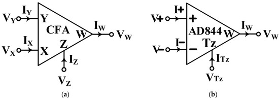
Figure 1.
The circuit symbol. (a) Current-feedback amplifier (CFA) and (b) AD844.
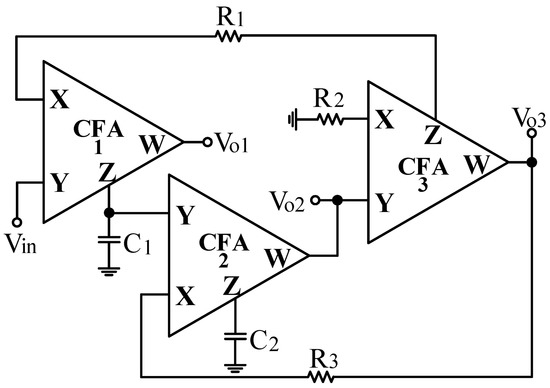
Figure 2.
Proposed CFA-based voltage-mode (VM) multifunction biquad filter.
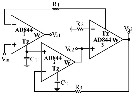
Figure 3.
CFA constructed using commercially available AD844 integrated circuits (ICs).
It can be seen from Equations (1) to (3) that Vo1 can obtain an NLP voltage response, Vo2 can obtain an IBP voltage response, and Vo3 can obtain an NBS voltage response. Hence, the proposed circuit can realize NLP, IBP, and NBS voltage responses simultaneously. The ωo and Q of the filter can be obtained by the following equations:
Hence, the filter parameters of ωo and Q offers orthogonal controllability.
3. Non-Ideal and Sensitivity Consideration
Practically CFA is characterized by the terminals equations VX = βVY, IZ = αIX, and VW = γVZ [14], where β, α and γ are port transfer ratios of the Y, X, and Z terminals, respectively. Taking into account the non-idealities, the denominator of the transfer functions of Figure 2 becomes
From Equation (6), the non-ideal ωo and Q in Equations (4) and (5) become
Sensitivity is an important performance of a biquad filter, and its formal definition can be expressed as follows:
where F represents one of ωo and Q. X represents any of the active parameter or passive component. Using this definition, the active and passive sensitivities with respect to ωo and Q can be obtained as
It is clearly observed from Equations (10) and (14) that the circuit has low passive and active sensitivity performances.
4. Simulation and Measurement Results
In order to confirm the theoretical study, the proposed circuit of Figure 2 was simulated using the AD844 macro-models of OrCAD PSpice version 17.2 and was experimented using commercial AD844AN of analog devices. The power supply voltage was given as ±6 V. The passive component values of the Figure 2 are given by R1 = R2 = R3 = 4 kΩ and C1 = C2 = 1 nF for the center frequency of fo = 39.79 kHz. Figure 4, Figure 5 and Figure 6 show the simulation and experimental gain-frequency and phase-frequency voltage responses for the NLP, IBP, and NBS filters of Figure 2, respectively. In the simulated NLP voltage response of Figure 4, the center frequency fo is 38.9 kHz, which is −2.23% different from the theoretical value. In the simulated IBP voltage response of Figure 5, the center frequency fo is 38.5 kHz, which is −3.24% different from the theoretical value. In the simulated NBS voltage response of Figure 6, the center frequency fo is 38.9 kHz, which is −2.23% different from the theoretical value. Figure 7 shows the different Q-values of IBP voltage response and the tunable Q-values, Q = 0.71, 1, and 2.5 are obtained without affecting the fo parameter. In Figure 7, R2 = R3 = 4 kΩ, C1 = C2 = 1 nF, and only vary the resistor R1 as 5.6, 4 and 1.6 kΩ. It is found that the total power consumption of the simulation is 255 mW. Figure 8, Figure 9 and Figure 10 represent the experimental frequency responses for the NLP, IBP, and NBS voltage responses of Figure 2, respectively. In the measured NLP voltage response of Figure 8, the center frequency fo is 41.364 kHz, which is 3.96% different from the theoretical value. In the measured IBP voltage response of Figure 9, the center frequency fo is 40.729 kHz, which is 2.36% different from the theoretical value. In the measured NBS voltage response of Figure 10, the center frequency fo is 41.036 kHz, which is 3.13% different from the theoretical value. The experimental gain-frequency voltage responses of the IBP filter with difference Q-values is shown in Figure 11. Figure 12 shows the experimental measurement result of the IBP transient response of the 40 kHz frequency and 2 V peak voltage of input voltage signal. It can be seen from the simulation and experimental results that they are consistent with the theoretical values.
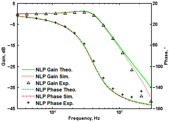
Figure 4.
Gain-frequency and phase-frequency voltage responses of the non-inverting low-pass (NLP) filter.
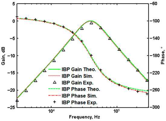
Figure 5.
Gain-frequency and phase-frequency voltage responses of the inverting band-pass (IBP) filter.
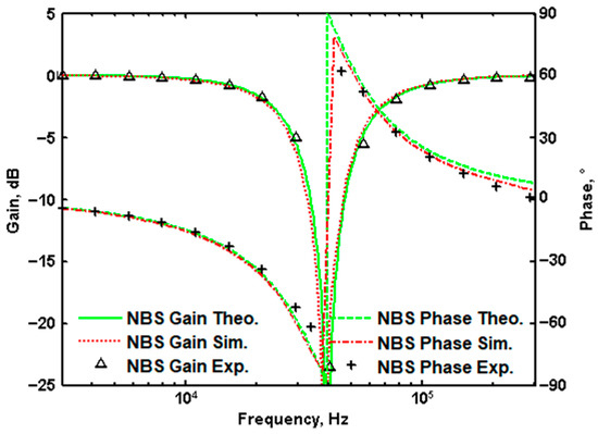
Figure 6.
Gain-frequency and phase-frequency voltage responses of the non-inverting band-stop (NBS) filter.
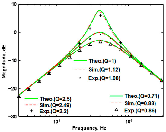
Figure 7.
Gain-frequency voltage responses of the IBP filter with different Q-values by changing resistor R1.
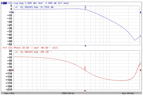
Figure 8.
Experimental gain-frequency and phase-frequency voltage responses of the NLP filter.
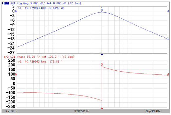
Figure 9.
Experimental Gain-frequency and phase-frequency voltage responses of the IBP filter.
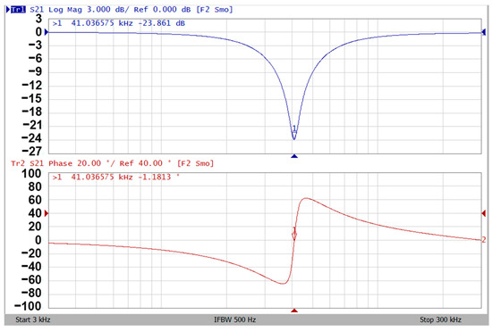
Figure 10.
Experimental Gain-frequency and phase-frequency voltage responses of the NBS filter.
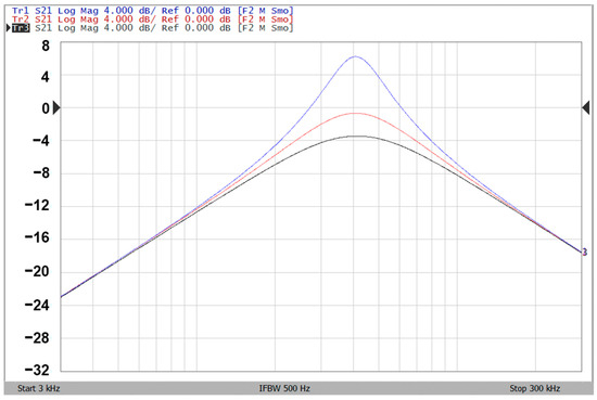
Figure 11.
Experimental gain-frequency voltage responses of the IBP filter with difference Q-values by changing resistor R1.
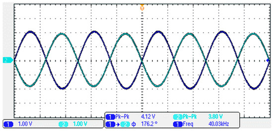
Figure 12.
Experimental measurement result of the IBP transient response for frequency 40 kHz and 2 V peak voltage of input voltage signal.
The 1-dB compression (P1dB) point is a key metric to determine the linear region of the circuit’s operation. This point represents that the input power reduces 1 dB gain from the normal linear gain specification. In general, there is nonlinearity in the transfer functions of all electronic circuits, and nonlinear distortion occurs. Hence, the third-order intercept (TOI) point measurement is a good indicator of the depth of distortion created by intermodulation products. Figure 13 and Figure 14 show the measurement results of the P1dB and the TOI point, respectively. The measured input P1 dB point is 18.8 dBm and the measure TOI point is 29.04 dBm.
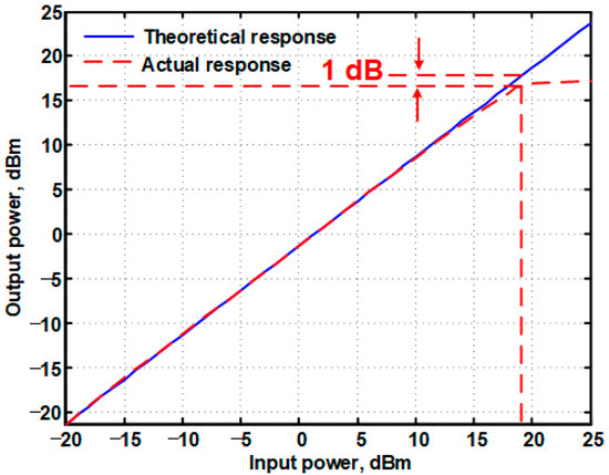
Figure 13.
P1dB point measurement of the IBP voltage response.
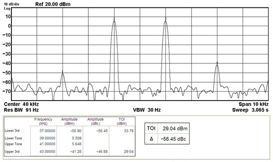
Figure 14.
Third-order intercept (TOI) point measurement of the IBP voltage response.
5. Conclusions
This paper presents a novel high-input impedance VM biquad filter with single input and triple outputs. The proposed circuit can realize NLP, IBP, and NBS voltage responses, simultaneously, by using three CFAs, two grounded capacitors and three resistors. The circuit has high input impedance, and therefore it can connect in cascade directly within VM biquad without additional voltage buffers. The circuit employs two grounded capacitors, which are easily implemented in the integrated circuit. The ωo and Q can be tuned orthogonally. The sensitivities of active and passive performances are low. The simulation and experimental results validate the theoretical analysis.
Author Contributions
S.-F.W. and H.-P.C. conceived and designed the theoretical verifications; Y.K. revised the manuscript to improve the quality of English; H.-P.C. analyzed the results and wrote the paper; Y.-F.L. performed the simulations and experiments. All authors have read and agreed to the published version of the manuscript.
Funding
This research was funded by the Ming Chi University of Technology.
Institutional Review Board Statement
Not applicable.
Informed Consent Statement
Not applicable.
Data Availability Statement
The data presented in this study are available on request from the corresponding author.
Conflicts of Interest
The authors declare no conflict of interest.
References
- Wang, S.F.; Chen, H.P.; Ku, Y.; Lee, C.L. Versatile voltage-mode biquadratic filter and quadrature oscillator using four OTAs and two grounded capacitors. Electronics 2020, 9, 1493. [Google Scholar] [CrossRef]
- Tran, H.D.; Wang, H.Y.; Lin, M.C.; Nguyen, Q.M. Synthesis of cascadable DDCC-based universal filter using NAM. Appl. Sci. 2015, 5, 320–343. [Google Scholar] [CrossRef]
- Herencsar, N.; Koton, J.; Hanak, P. Universal voltage conveyor and its novel dual-output fully-cascadable VM APF application. Appl. Sci. 2017, 7, 307. [Google Scholar] [CrossRef]
- Maheshwari, S.; Chaturvedi, B. High-input low-output impedance all-pass filters using one active element. IET Circuits Devices Syst. 2012, 6, 103–110. [Google Scholar] [CrossRef]
- Lee, C.N. Independently tunable plus-type DDCC-based voltage-mode universal biquad filter with MISO and SIMO types. Microelectron. J. 2017, 67, 71–81. [Google Scholar] [CrossRef]
- Psychalinos, C.; Kasimis, C.; Khateb, F. Multiple-input single-output universal biquad filter using single output operational transconductance amplifiers. AEU Int. J. Electron. Commun. 2018, 93, 360–367. [Google Scholar] [CrossRef]
- Zhang, C.; Shang, L.; Wang, Y.; Tang, L. A CMOS programmable fourth-order butterworth active-RC low-pass filter. Electronics 2020, 9, 204. [Google Scholar] [CrossRef]
- Liu, S.I.; Wu, D.S. New current-feedback amplifier-based universal biquadratic filter. IEEE Trans. Instrum. Meas. 1995, 44, 915–917. [Google Scholar]
- Horng, J.W. New configuration for realizing universal voltage-mode filter using two current-feedback amplifiers. IEEE Trans. Instrum. Meas. 2000, 49, 1043–1045. [Google Scholar] [CrossRef]
- Tangsrirat, W.; Surakampontorn, W. Single-resistance-controlled quadrature oscillator and universal biquad filter using CFOAs. AEU Int. J. Electron. Commun. 2009, 63, 1080–1086. [Google Scholar] [CrossRef]
- Shah, N.A.; Iqbal, S.Z.; Rather, M.F. Versatile voltage-mode CFA-based universal filter. AEU Int. J. Electron. Commun. 2005, 59, 192–194. [Google Scholar] [CrossRef]
- Shan, N.A.; Rather, M.F.; Iqbal, S.Z. CFA-based three input and two outputs voltage-mode universal filer. Indian J. Pure Appl. Phy. 2005, 43, 636–639. [Google Scholar]
- Singh, V.K.; Singh, A.K.; Bhaskar, D.R.; Senani, R. New universal biquads employing CFOAs. IEEE Trans. Circuits Syst. II Express Briefs 2006, 53, 1299–1303. [Google Scholar] [CrossRef]
- Horng, J.W. Voltage-mode universal biquad with five inputs and two outputs using two current feedback amplifiers. Indian J. Eng. Mater. Sci. 2013, 20, 87–91. [Google Scholar]
- Chang, C.M.; Hwang, C.S.; Tu, S.H. Voltage-mode notch, lowpass and bandpass filter using current-feedback amplifiers. Electron. Lett. 1994, 30, 2022–2023. [Google Scholar] [CrossRef]
- Shah, N.A.; Malik, M.A. Multifunction filter using current feedback amplifiers. Frequenz 2005, 59, 264–267. [Google Scholar] [CrossRef]
- Nikoloudis, S.; Psychalinos, C. Multiple input single output universal biquad filter with current feedback operational amplifiers. Circuits Syst. Signal Process. 2010, 29, 1167–1180. [Google Scholar] [CrossRef]
- Topaloglu, S.; Sagbas, M.; Anday, F. Three-input single-output second-order filters using current-feedback amplifiers. AEU Int. J. Electron. Commun. 2012, 66, 683–686. [Google Scholar] [CrossRef]
- Singh, A.K.; Senani, R. CFOA-based state-variable biquad and its high-frequency compensation. IEICE Electron. Express 2005, 2, 232–238. [Google Scholar] [CrossRef]
- Horng, J.W.; Lee, M.H. High input impedance voltage-mode lowpass, bandpass and highpass filter using current-feedback amplifiers. Electron. Lett. 1997, 33, 947–948. [Google Scholar] [CrossRef]
- Shan, N.A.; Malik, M.A. High input impedance voltage-mode lowpass, bandpass, highpass and notch filter using current feedback amplifiers. Indian J. Eng. Mater. Sci. 2005, 12, 278–280. [Google Scholar]
- Shan, N.A.; Malik, M.A. New high input impedance voltage-mode lowpass, bandpass and highpass filter using current feedback amplifiers. J. Circuits Sys. Comp. 2005, 14, 1037–1043. [Google Scholar]
- Wang, S.F.; Chen, H.P.; Ku, Y.; Chen, P.Y. A CFOA-based voltage-mode multifunction biquadratic filter and a quadrature oscillator using the CFOA-based biquadratic filter. Appl. Sci. 2019, 9, 2304. [Google Scholar] [CrossRef]
- AD844: 60 MHz, 2000 V/μs, Monolithic op amp with Quad Low Noise Data Sheet (Rev. G). May 2017. Available online: www.linear.com (accessed on 1 December 2020).
Publisher’s Note: MDPI stays neutral with regard to jurisdictional claims in published maps and institutional affiliations. |
© 2021 by the authors. Licensee MDPI, Basel, Switzerland. This article is an open access article distributed under the terms and conditions of the Creative Commons Attribution (CC BY) license (http://creativecommons.org/licenses/by/4.0/).