1. Introduction
The model of Mealy finite state machine (FSM) is used very often in the process of designing control units of modern digital systems [
1,
2,
3]. There are many problems connected with optimization of characteristics of control units [
4,
5]. One of the most important problems is a problem of hardware reduction [
6,
7].
Solution of this problem allows reducing the power consumption and increasing the performance (maximizing operating frequency) [
8,
9]. To solve this problem, it is necessary to take into account the specific features of both an FSM model and logic elements used to implement the circuit of FSM [
3,
10].
The main specific of Mealy FSM is a dependence of input memory functions and output functions on both input variables and state variables [
1,
8]. Our investigation of standard benchmarks [
11] shows that it could be up to 17 arguments in Boolean functions representing FSM circuits.
Presently, the field-programmable gate array (FPGA) chips are widely used for implementing different digital systems [
8,
12,
13]. Of course, FPGAs also are used to implement control units of these systems. There are three main elements of FPGA which could be used to implement FSM circuits. They are: look-up table (LUT) elements, embedded memory blocks (EMB) and tools of programmable interconnections [
14,
15,
16]. LUTs fit for implementing Boolean functions represented as sum-of-products (SOP) [
8]. EMBs implement large truth tables representing systems of Boolean functions (SBF).
A LUT is an array of SRAM cells with
inputs (
[
13,
14]. Outputs of LUTs are connected with programmable flip-flops which could be bypassed. Therefore, it is possible to implement distributed registers keeping state codes [
3].
An EMB is a RAM with
address inputs and
outputs. The main specific of EMBs is their reconfigurability [
3]. It means that the values of
and
could be changed. Of course, the number of bits (the volume of EMB) is constant. It is determined as
Due to the reconfigurability, it is possible to tune EMBs to meet the requirements of a particular design. There are the following pairs
[
13]:
,
,
,
,
,
and
. It gives
, bits.
In this article, we propose a method of synthesis leading an FSM circuit to implemented as a network of EMBs and LUTs. The method is based on the structural decomposition [
17] of FSM circuit.
2. Background of Mealy FSMs
The logic circuit of Mealy FSM is represented by the following systems of Boolean functions [
1]:
In (
2) and (
3), there are the following sets:
is a set of input memory functions,
is a set of state variables,
is a set of input variables,
is a set of output functions.
To find systems (
2) and (
3), it is necessary to specify a behaviour of FSM. In this article, we use a state transition table (STT) to represent a Mealy FSM. An STT contains information about the transitions between internal states
, where
is a set of states [
8]. There are the following columns in an STT:
is a current state;
is a state of transition;
is a conjunction of input variables (or their complements) determining the transition
;
is a collection of output functions (COF) generated during the transition
;
h is a number of transition
. For example, consider some Mealy FSM
represented by STT (
Table 1).
The following sets and their parameters could be derived from
Table 1:
,
,
,
,
,
. There are
rows in
Table 1. To find the sets
and
T, it is necessary to encode the states
by binary codes
with
R bits. It is a step of state assignment [
8]. Let us use minimum number of state variables when there is
In the discussed case, there is . It gives the sets and . As follows from the set , we use D flip-flops to implement the register.
To get functions (
2) and (
3), it is necessary to turn an STT into a direct structure table (DST) [
1] of Mealy FSM. To do it, we should add three columns into an STT, namely:
is a code of current state;
is a code of state of transition;
is a collection of input memory functions equal to 1 to replace
by
.
Each row of DST corresponds to a product term
. The term
is the following conjunction:
The first member of (
5) is a conjunction
of state variables corresponding to the code
of the state
from the h-th row of
. There are
,
,
. The symbol
stands for the value of the r-th bit of
.
The functions (
2) and (
3) depend on terms (
5). The system (
2) determines a block of input memory functions (BIMF), the system (
3) the block of output functions (BOF). State codes are kept into
. It determines a Mealy FSM
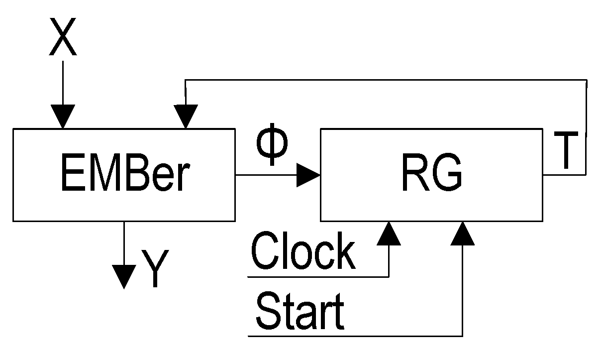
(
Figure 1). The pulse
loads the code
of the initial state
into
. The pulse
allows changing the content of RG.
3. Implementing Mealy FSMs with FPGAs
Each block of FSM
could be implemented using either LUTs or EMBs. We name the block of LUTs as LUTer, the block of EMBs as EMBer. In the simplest case, we have a LUT-based FSM
(
Figure 2).
Let an FSM circuit be represented by
I Boolean functions. There is
in the case
. Let the following condition take place:
In (
6), the symbol
stands for the number of literals in a SOP of
.
In this case, there are exactly
I LUTs in the circuit of
. If the condition (
6) is violated, then some functions should be decomposed. To do it, the different methods of functional decomposition are used [
18,
19,
20]. It leads to multi-level circuits with complex interconnections. The multi-level circuits of LUTers consume more energy and have less performance than their single-level counterparts.
It is very important to use EMBs in FSM design. It decreases the chip area occupied by FSM circuit, as well as the number of interconnections [
21,
22,
23]. In turn, it results in decreasing for both the power consumption and propagation time (as compared to LUT-based counterparts). Because of it, there is a lot of EMB-based methods of Mealy FSMs synthesis [
10,
16].
Let the following condition take place:
In this case, it is enough a single EMB to implement the circuit of
. It leads to FSM
(
Figure 3).
If condition (
7) is violated, then EMBer is implemented as a network of EMBs. It has sense till the following conditions take places:
If condition (
8) is violated, then some methods of structural decomposition [
16,
17] could be used to diminish the values of
.
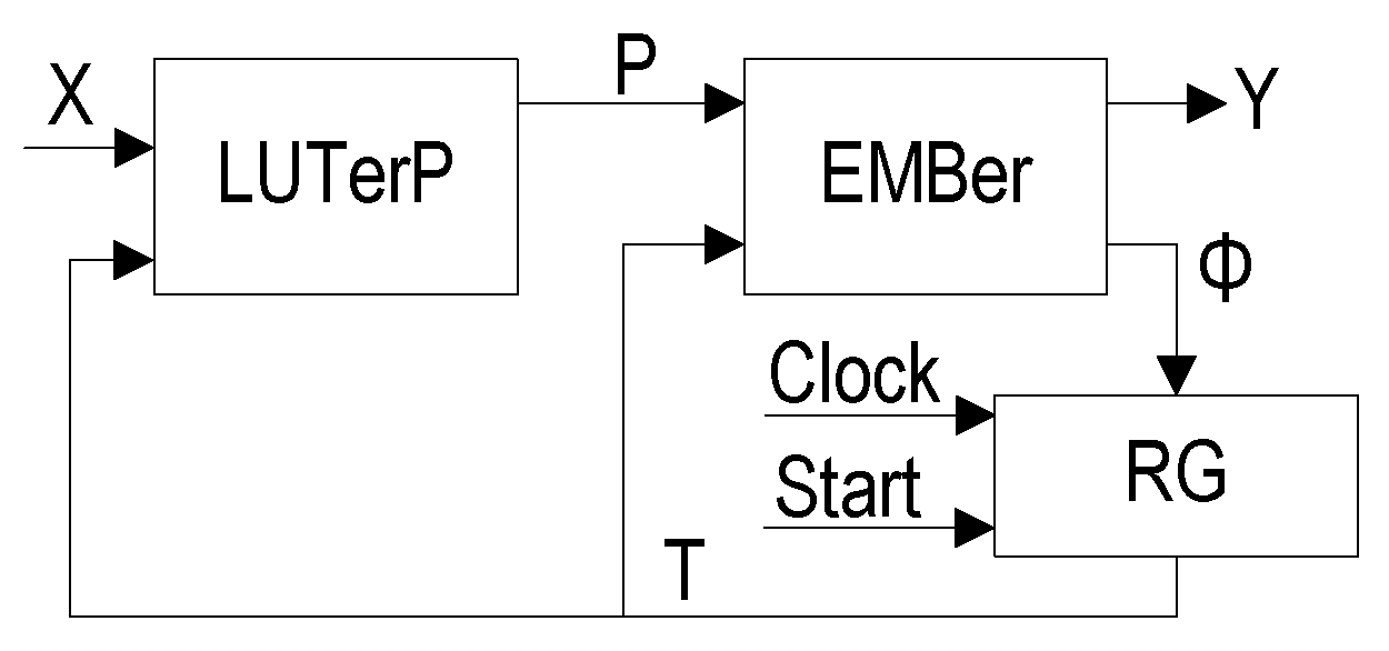
As a rule, the method of replacement of input variables is used [
1,
10]. In this case, the variables
are replaced by variables
. In many practical cases, there is
[
2]. Our analysis of standard benchmarks [
16] justifies this statement. In this case, three following SBFs represent the FSM circuit:
As a rule, the system (
10) is implemented by LUTs [
10,
21]. The systems (
11) and (
12) are implemented by EMBs. It leads to Mealy FSM
(
Figure 4).
To find the system (
10) it is necessary: (1) to construct the set
P; (2) to execute the replacement of
; (3) to encode the states and (4) to construct the table of LUTerP. To find the systems (
11) and (
12), it is necessary to transform the initial DST of
. The transformation is reduced to: (1) the replacement
by
and (2) the replacement of the column
by the column
.
Let us use the symbol
to show that the model
is used to synthesize an FSM circuit starting from the STT of FSM
. Let us find the system (
10) for FSM
.
As follows from
Table 1, there are transitions depended on a single variable
or two variables. Therefore, there is
. It gives
. There is
,
. Let us encode the states of
in the trivial way:
. The replacement
is represented by
Table 2. It is constructed using the rules [
1].
After minimizing, we can find the following equations:
Obviously, a proper state assignment could diminish the number of arguments in functions (
10). These methods are discussed in [
1,
10].
Let the following condition take place:
In this case, it is enough a single EMB to implement the circuit of EMBer of FSM .
There are other methods of structural decomposition [
10]. For example, there are such methods as: (1) the encoding of collections of output functions; (2) the encoding of terms of DST; (3) the transformation of object codes. In this article, we discuss the using the encoding of terms in EMB-based Mealy FSMs. This method was used in FSMs implemented with programmable logic arrays [
1]. It has never been used in FPGA-based design.
Let us explain this approach. Let us encode a term
by a binary code
with
bits, where
Let us use variables
for the encoding, where
. Let us construct the following SBFs:
Let the following condition take place:
Let the condition (
7) is violated. In this case, we propose the FSM
(
Figure 5). In this FSM, the EMB implements the system (
16), the LUTer
the system (
17) and the LUTerY the system (
18).
Let the following condition take place:
In this case, there are LUTs in the FSM circuit. Both LUTers have only a single level of LUTs.
However, if the condition (
20) is violated, it is necessary to use the functional decomposition of functions (
17) and (
18). In this article, we discuss a case when the condition (
20) is violated. Also, we discuss the additional condition: we could use only a single EMB. This restriction could be connected with the fact that other EMBs are taken for implementing other parts of a digital system.
As a rule, it is very important to choose the state codes leading to minimizing the values of
[
8]. There are a lot of methods of state assignment targeting FPGA-based design [
17,
18,
19,
20,
21,
24,
25]. There is an opinion that JEDI [
8] is the best of them [
4]. But in the case of
there is no influence of state codes on the hardware amount. Therefore, we do not analyze the state assignment methods in this article.
4. Main Idea of Proposed Method
Let a Mealy FSM be represented by an STT with H rows. Let us possess only a single EMB to implement the FSM circuit. Let us have FPGA chip with LUTs with inputs. Let the terms form a set . Let us use the encoding of terms to reduce the number of LUTs in the FSM circuit.
Let us find the value of
K for given STT and value of
, where:
Let us discuss a case, when . It means that . Therefore, both LUTerΦ and LUTerY of are represented by multi-level circuits.
In this article, we propose a method allowing: (1) to diminish the number of LUTs in comparison with equivalent FSM
and (2) to regularize the interconnections. The method is based on dividing the initial STT by
K sub-tables with up to
rows. Let us illustrate this method using the STT of
(
Table 1).
Let us use an EMB such that the condition (
7) is violated for
. Let the EMB have the configuration
such that the following conditions are true:
The condition (
22) shows that it is enough a single EMB to implement SBF (
16). The condition (
23) shows that it is not possible to implement an FSM circuit using a single EMB.
Let us find a partition
of the set
F such that the following condition takes place:
Let it be
elements in the set
. The value of
is determined as:
Each class
determines sets
and
. The set
includes states of transition written in the rows of STT corresponding to the class
. The set
includes output functions written in the rows of STT corresponding to the
. Let us find such a partition
that
In (
26) and (
27), there is
and
.
Let us encode the term
by a binary code
with
bits. Let us use variables
for the encoding. These variables are the same for all classes
. To distinguish the classes, let us encode classes
by binary codes
with
bits:
Let us use the variables to encode the classes, where .
Now, the code
is represented as
where * is a sign of concatenation. Of course there is
.
Let the following condition take place:
In this case, some functions
and
could be implemented by EMB. Let they form sets
and
, respectively. Therefore, LUTs should be used for implementing the remained functions. Let it be
and
. Using these preliminaries, we propose the model of Mealy FSM
(
Figure 6).
In FSM
, the EMB generates functions (
16) and the following SBFs:
The LUTerk
generates functions:
The LUTerΦY implements functions
and
where
In (
36) and (
37) the superscript
k means that the corresponding function is generated by LUTerk. The
is a Boolean variable equal 1 if and only if
,
. Also, functions
enter LUTerΦY. Each function requires a flip-flop, so it uses a single LUT. The symbol
stands for the conjunction corresponding to
:
In (
38),
is a value of the r-th bit of
,
,
,
.
Because the condition (
24) is true, there are
LUTs in the circuit of LUTerk. If conditions (
26) and (
27) take places, the number of LUTs in LUTer1-LUTerK is minimized.
Assuming that a Mealy FSM S is represented by an STT, we propose the following design method for FSM :
Creating the partition
corresponding to (
26) and (
27).
Executing the state assignment.
Creating the DST of Mealy FSM.
Creating the sets , , and .
Encoding of terms and classes of .
Creating the systems (
34) and (
37).
Transformation of DST.
Creating the table of EMB.
Implementing FSM circuit with particular EMB and LUTs.
The number of LUTs in are mostly determined by the partition . Let us discuss how to find the partition .
5. Constructing Partition of the Set of Terms
The problem is formulated as the following. It is necessary to find the partition
with
K blocks such that relations (
26) and (
27) take places. The value of
K is determined by (
21).
In this article, we propose a simple sequential algorithm for solution of this problem. We characterize each term by two sets. The set includes output functions written in the h-th row of STT. The set includes a state of transition from the h-th row of STT. If , then and . Of course, the set is determined by the codes of states .
We use two evaluations in this algorithm. The evaluation
determines how many new output functions will be added to
due to including
into
. We determine these evaluations as the following:
There are
insignificant assignments of variables
:
They could be used for minimizing function (
34) and (
35). We propose to distribute terms evenly among
K groups. It corresponds to the vector
. Therefore, each class
includes
elements, where:
There are two stages in generating each block
. Let
blocks be constructed. At the first stage, we should choose the basic element (BE)
, where there is
. The term
is a BE of
if it satisfies to the following relation:
If the condition (
43) is true for terms
and
, the we choose the term
where
.
The second stage has
steps. At each step, we should choose the next element of
. To do it, we use the following approach. Let us form a set
including terms
such that
. Let us select a term
such that
If more than a single term satisfies to (
44), then we should choose the term with the following property:
If there are several terms with the property (
45), we choose a term with the less value of
h. Next, we should make
and eliminate the term
from
.
The constructing is terminated if: (1) all terms are already distributed or (2) there are elements in .
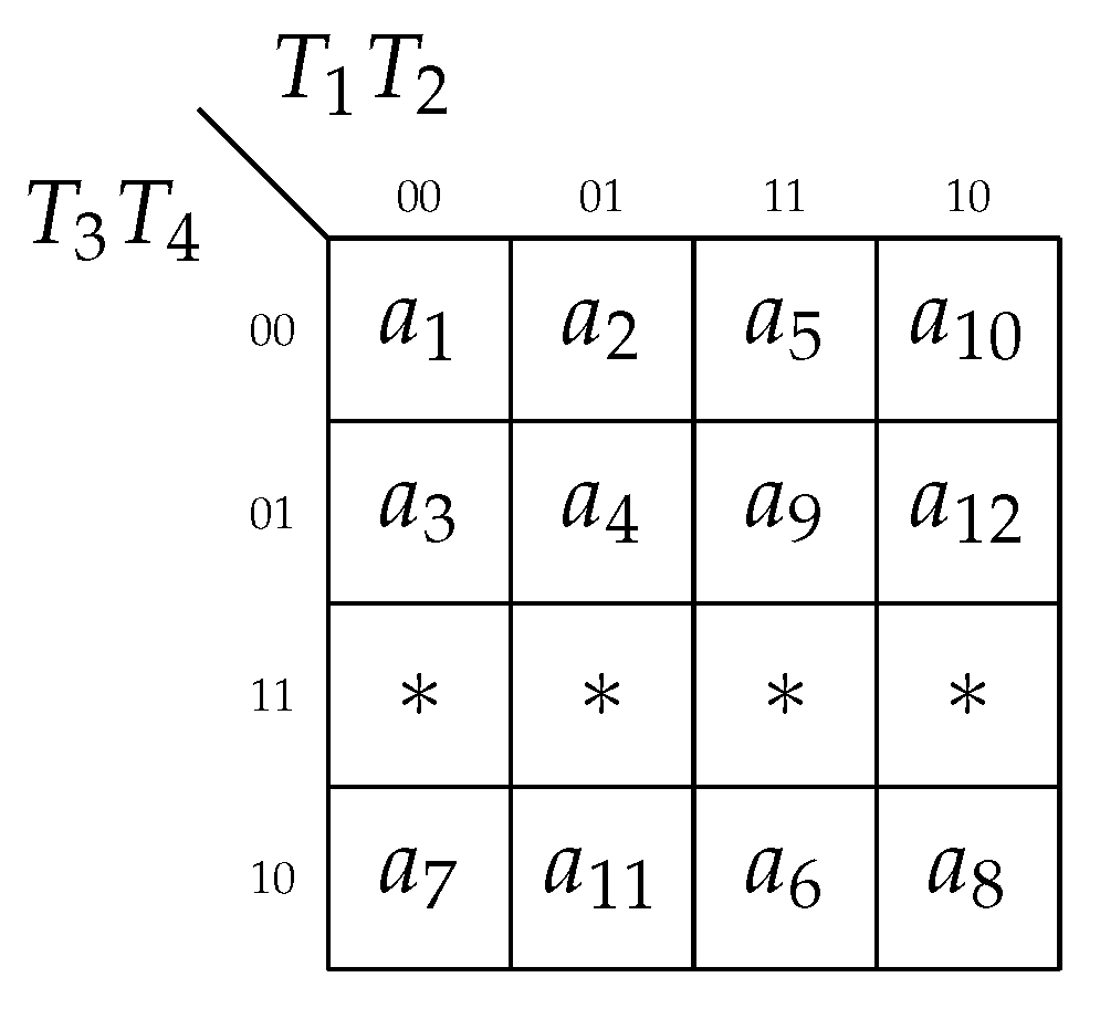
Let us discuss an example of creating the partition
for Mealy FSM
. Let it be
. Using (
21) gives
. Using (
41) gives
. Let us form the vector
. It gives
,
. The process is shown in
Table 3.
Let us explain columns of
Table 3. There are terms
in the column
h. The column
contains the numbers of output functions in terms
. There are basic elements of
and
shown in columns BE1 and BE2, respectively. The symbol
I stands for (
39), the symbol
for (
40). The sign ⊕ means that a particular term is chosen as a basic element. The sign “−” means than
. The sign “+” means that the corresponding term is included into the class
. There are terms
in the row
. They are shown in the order of their selection. There are output functions
in the row
, the states
in the row
. We determine the evaluation (
40) only for terms with equal values of (
39).
As follows from
Table 3, there are
steps in the process of selection. The class
includes terms
. Our approach allows constructing the partition
with the following classes:
,
and
. It gives the following sets:
,
and
,
,
,
,
,
,
. Therefore, there are the following results for (
26) and (
27):
,
,
,
,
,
.
6. Example of Synthesis
In
Section 5, we found the partition
for the discussed example. Let us use an EMB including the configuration
. Therefore, there is
and
. There is
for FSM
. The condition (
22) takes place. There is
and
. Using (
21) gives
: so, there is
and
obviously,
. Also, there is
. Because
, the condition (
23) takes place. Therefore, it is possible to use the model
for FSM
. Therefore, let us design the FSM
.
Let us execute the state assignment allowing a reduction to the numbers of elements in the sets
. One of the possible solutions is shown in
Figure 7.
Using
Figure 7 and sets
gives the sets
. They are the following:
,
and
.
Using
Table 1 and codes form
Figure 7, we can construct the direct structure table of FSM
. It is
Table 4. To construct the transformed DST, it is necessary to find codes
and
.
Let us construct the sets
,
,
and
. To do it, we should find the value of
. There are
and
. Using (
30) gives
. We should eliminate functions
and
which belong to
K corresponding sets. In the discuss case, there is
. Therefore, let us form the sets
and
. Obviously, there are
and
. Now, we have the sets
,
and
. Of course, there are the sets
,
and
.
Let us construct the systems of Boolean functions shoving dependence of functions
and
on the terms
. To do it, we use the DST (
Table 4) and classes
. We could find the following systems:
Let us encode the terms
in such a manner that there is minimum number of literals in systems (
46) and (
48). We could get codes shown in
Figure 8.
Using the system (
46) and Karnaugh map (
Figure 8a), we could form the following system:
The system (
49) represents the circuit of LUTer1. It includes 4 LUTs and has 9 interconnections with the EMB.
Using the system (
47) and Karnaugh map (
Figure 8b), we could form the following system:
The system (
50) represents the circuit of LUTer2. It includes 4 LUTs and has 9 interconnections with the EMB.
Using the system (
49) and Karnaugh map (
Figure 8c), we could form the following system:
The system (
51) represents the circuit of LUTer3. It includes 5 LUTs and has 10 interconnections with the EMB.
Let us encode the classes
as the following:
,
and
. It gives the conjunctions
,
and
. Using these codes and Equations (
49) and (
51), we could find the systems (
36) and (
37). They are the following:
As follows from the system (
52), it is necessary to transform the equations for
and
. But we can escape it using the following approach. There is
. Let us multiply it by
. It gives
. Now, we could represent
as
with
. So, now it is enough a single LUT for implementing the function
. The same could be done for
. But it is necessary to apply the rules of functional decomposition for functions
and
. For example, there are two LUTs in the circuit for
(
Figure 9).
The equation is represented as , where . The equation for will be the following: . Here . Therefore, there are two LUTs in the circuit of .
To find the systems (
16) and (
31), it is necessary to transform the DST of Mealy FSM
. To transform the DST, it is necessary to delete the column
,
,
and
. They are replaced by the following columns:
,
,
,
,
and
. The column
includes the variables
equal to 1 in the code
from the h-th row of transformed DST. The column
includes the variables
equal 1 in the code
of the term
. The column
includes the functions
generated during the h-th transition of FSM. The column
contains the variables
equal to 1 in the h-row of initial DST. In the discussed case, there is
. So, the column
is absent in the transformed table of Mealy FSM
(
Table 5).
To implement the functions
,
,
and
, it is necessary to construct the table of EMB. It contains the following columns:
,
X,
Z,
V,
,
,
q. The addresses of cells are determined by concatenations of
and
X. The table includes
rows:
It is necessary
rows to represent transitions from a state
, where
Using (
54) and (
55) gives
and
for
. The first 8 rows of table of EMB is shown in
Table 6. These rows represent transitions from the state
. There is
for these rows. Therefore, these 8 rows correspond to
from
Table 5. Due to
, we do not show the column
in
Table 5.
7. Experimental Results
To investigate the efficiency of proposed method, we use standard benchmarks from the library [
11]. The library includes 48 benchmarks taken from the design practice. The benchmarks are rather simple, but they are very often used by different studies to compare new and known results [
26]. The benchmarks are represented in KISS2 format. The characteristics of benchmarks are shown in
Table 7.
We used our CAD tool K2F [
26] to translate KISS2 –based files into VHDL-based FSM models. Next, the Active-HDL environment was used to synthesize and simulate FSMs. To get FSM circuits, we used Xilinx CAD tool Vivado [
27]. The FPGA chip XC7VX690TFFG1761-2 by Vertex-7 [
28] was used as a target platform. The chip includes LUTs with 6 inputs and EMBs with configurations from
till
.
We presume that only a single EMB is available to implement an FSM circuit. As follows from
Table 7, the condition (
7) takes place for 33 benchmark FSMs (it is around 68% from all benchmarks). Therefore, it is necessary only a single EMB to implement an FSM circuit for these benchmarks. We mark this situation by the sign “+” in the column “EMB” of
Table 7. Also, we show in this column pairs
corresponding to the configuration required to implement the circuit with a single EMB. The further research was conducted for these 15 benchmarks.
Three discussed methods (
,
and
) were taken to compare with our approach (
). The results are shown in
Table 8 (the number of LUTs in FSM circuits),
Table 9 (the operating frequency) and
Table 10 (the consumed energy). To design FSM
, a single EMB was used to implement a part of FSM circuit. We do not know which part of a circuit was implemented as an EMB. It is up to Vivado and cannot be directly specified by a designer.
Table 8,
Table 9 and
Table 10 are organized in the same order. The rows are marked by the names of benchmarks, the columns by design methods. The rows “Total” include results of summation for values from corresponding columns. The summarized characteristics of
-based FSMs are taken as 100%. The rows “Percentage” show the percentage of summarized characteristics respectively to
-based benchmarks. To design all circuits, we use the mode AUTO of Vivado.
As follows from
Table 8, the
-based FSMs require fewer LUTs than their counterparts based on other FSM models. There is the following economy: (1) 23% regarding
; (2) 4% regarding
; (3) 45% regarding
. Therefore, for these benchmarks the
-based FSMs require the largest number of LUTs. It is connected with the fact that the condition (
20) is violated for all considered
-based benchmarks. It results in multi-level circuits implementing functions (
17) and (
18).
As follows from
Table 9, the
-based FSMs have the highest operating frequency as compared to other investigated FSMs. We think that this is due to the smaller number of logic levels and inter-level connections compared to other investigated FSMs. But we cannot prove this statement because Vivado does not show these details about implemented circuits. There is the following gain in operating frequency: (1) 32.6% regarding
; (2) 44.3% regarding
; (3) 27.8% regarding
. The lowest frequency takes place for
–-based FSMs. It is connected with rather big amount of inputs. Because
, the circuit of LUTerP is multi-level. For discussed benchmarks, the number of logic levels in
-based FSMs is higher than it is for FSMs produced by other investigated methods.
As follows from
Table 10, the
-based FSMs consume less energy than their counterparts based on other FSM models. There is the following economy: (1) 39.8% regarding
; (2) 51% regarding
; (3) 11.4% regarding
. It is connected with the fact that
-based FSM circuits have fewer LUTs and, therefore, interconnections compared to other investigated FSMs. Interconnections are known to be responsible for up to 70% of energy losses in FPGA-based circuits [
26]. The results shown in
Table 10 include the total power value in Watts. It should be noted that the total power consists of individual powers such as: static power, I/O, signals, LUT as Logic, F7/F8 Muxes, BUFG, registers and others. Furthermore, the frequency has a very strong impact to the power consumption.
Therefore, our approach produces better results for FSMs whose circuits cannot be implemented as a single EMB. Of course, this conclusion is true only for the benchmarks [
11] and the device XC7VX690TFFG1761-2. It is almost impossible to make similar conclusion for the general case.
8. Conclusions
Contemporary FPGA devices include a lot of look-up table elements. It allows the implementation of very complex digital system using only a single chip. But LUTs have rather small amount of inputs (
does not exceeds 6). This value is considered to be optimal [
6]. Such a limitation leads multi-level circuits representing, for example, sequential blocks of digital systems. To design multi-level circuits, the methods of functional decomposition are used. But these blocks can be synthesized using different methods of structural decomposition. As our studies [
26] show, the structural decomposition can lead to FSM circuits with better characteristics than their counterparts based on functional decomposition.
The aim of this article is a presentation of a novel method of logic synthesis targeting Mealy FSMs implemented with LUTs and a configurable EMB. It is the method of structural decomposition based on encoding of product terms of Boolean functions representing FSM logic circuits. The essence of our approach is a splitting of the set of terms in a way minimizing the number of LUTs in FSM circuits. The proposed method is technology depended because it takes into account the number of inputs of LUT elements.
The experiments conducted using the Xilinx CAD tool Vivado 2019.1 clearly show that the proposed approach leads to reduction for such values as the number of LUTs, propagation time and consumed energy in comparison with FSM circuits based on known methods of terms encoding.
There are three directions in our future research. The first is connected with development design methods targeting FPGA chips of Intel (Altera). The second direction is connected with using our approach in real devices such as PDMS micro-optofluidic chip [
29,
30]. The last direction targets sequential blocs represented by Moore FSMs.


