Evaluation of the Potential Electromagnetic Interference in Vertically Stacked 3D Integrated Circuits


Abstract
Featured Application
Abstract
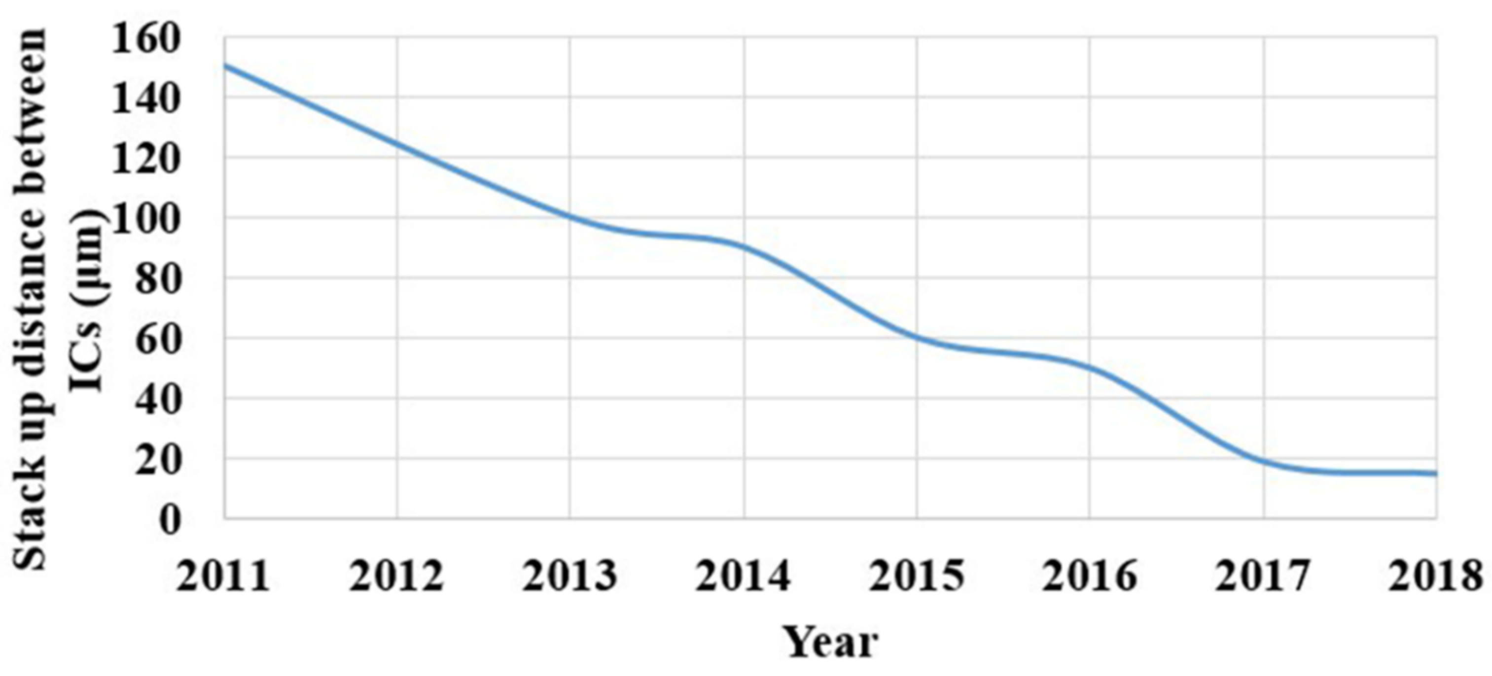
1. Introduction
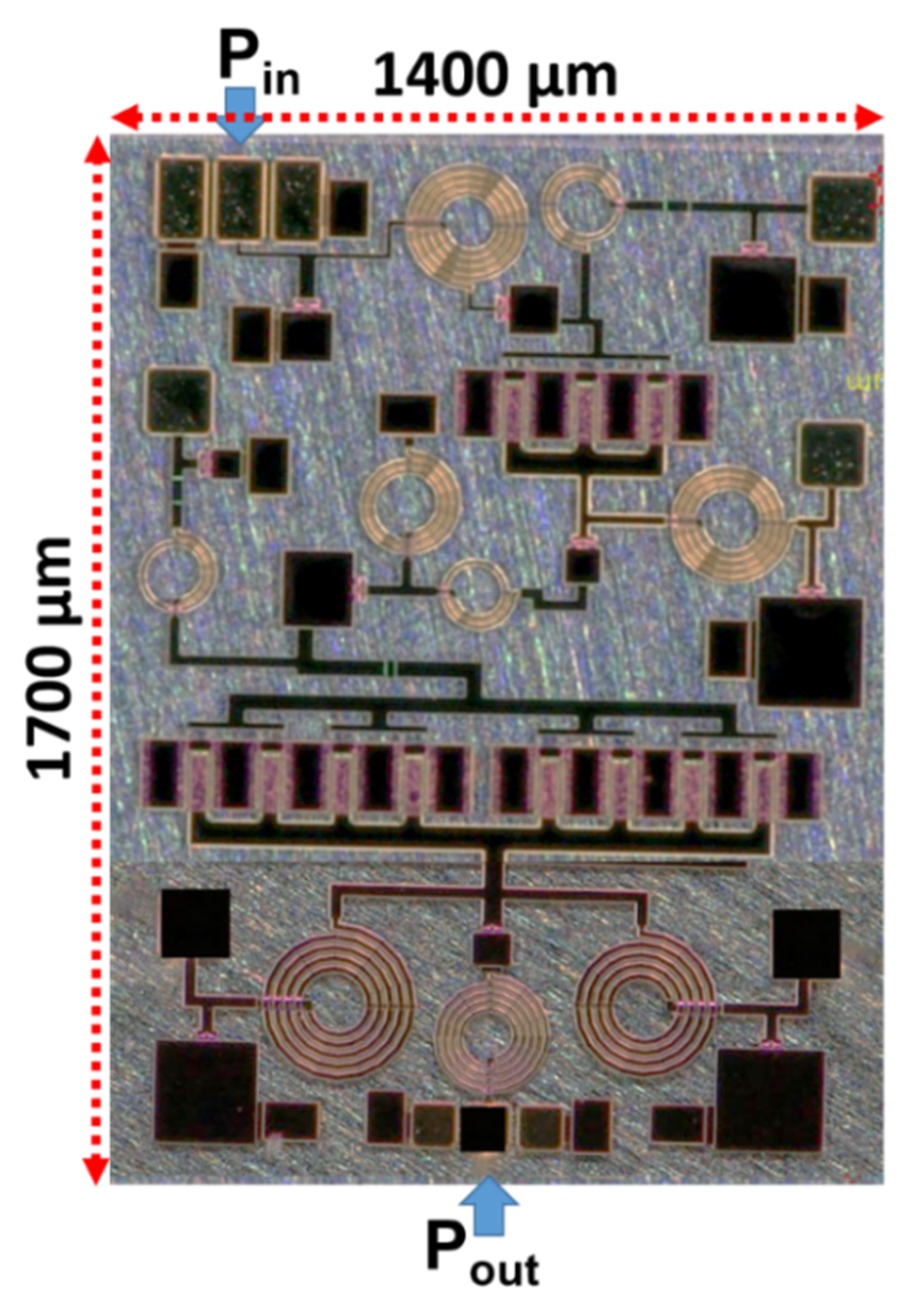
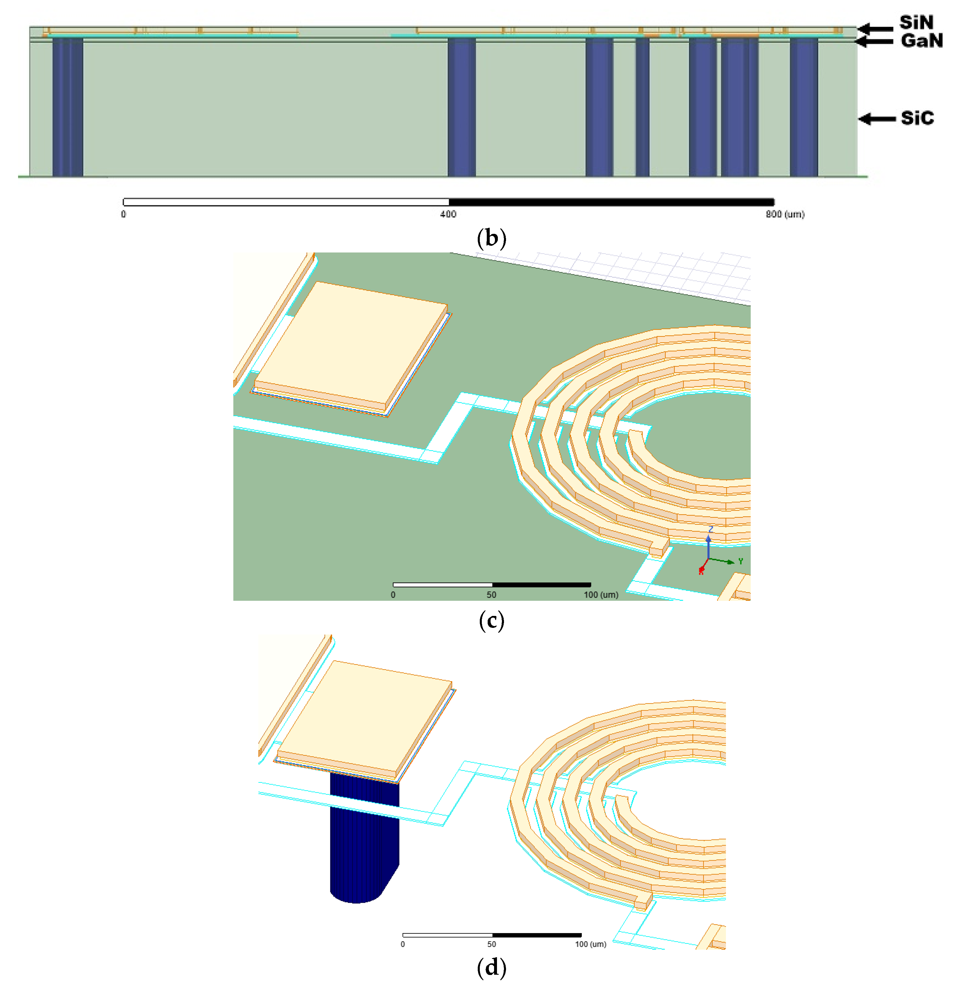
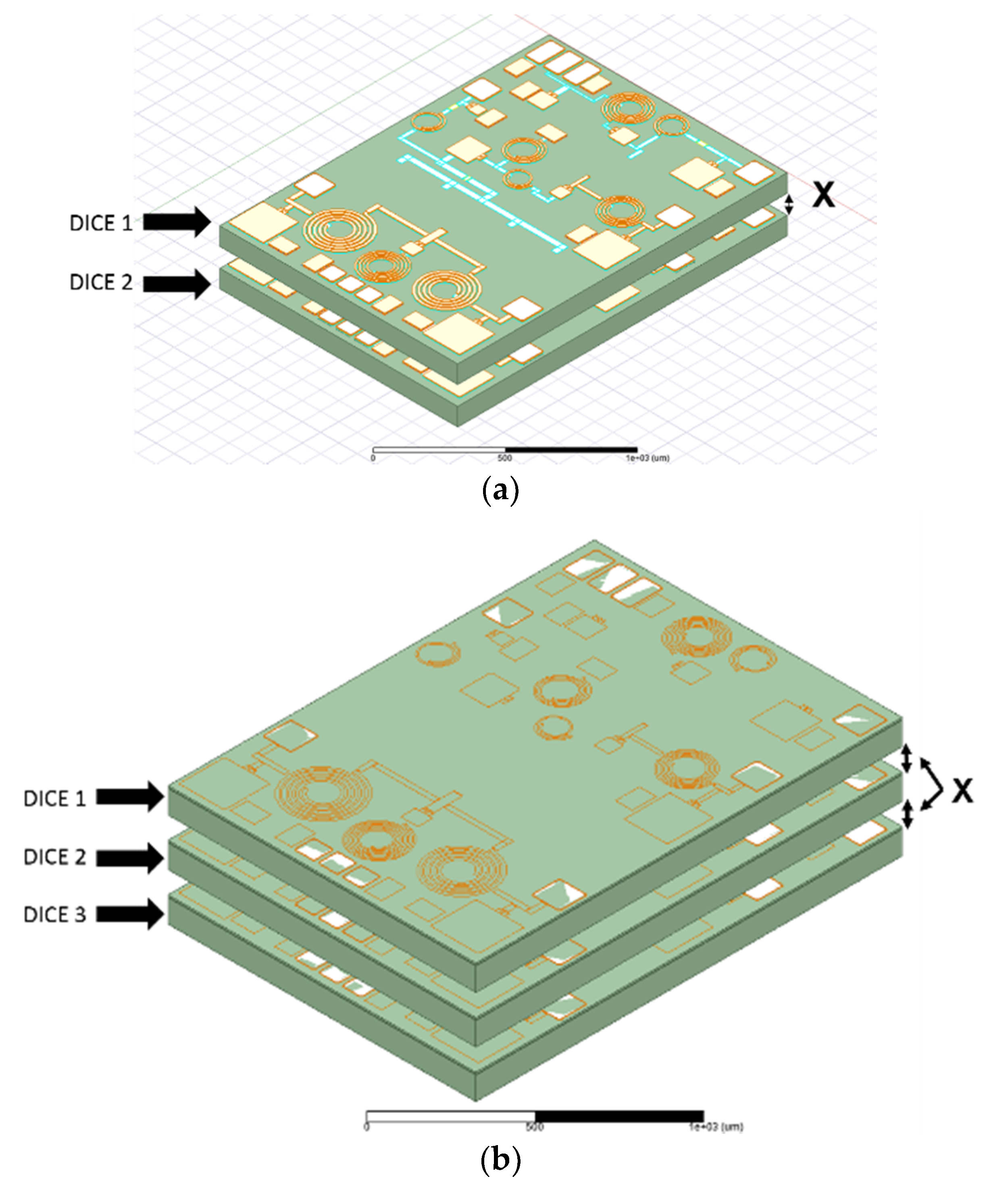
2. Integrated Circuit under Study
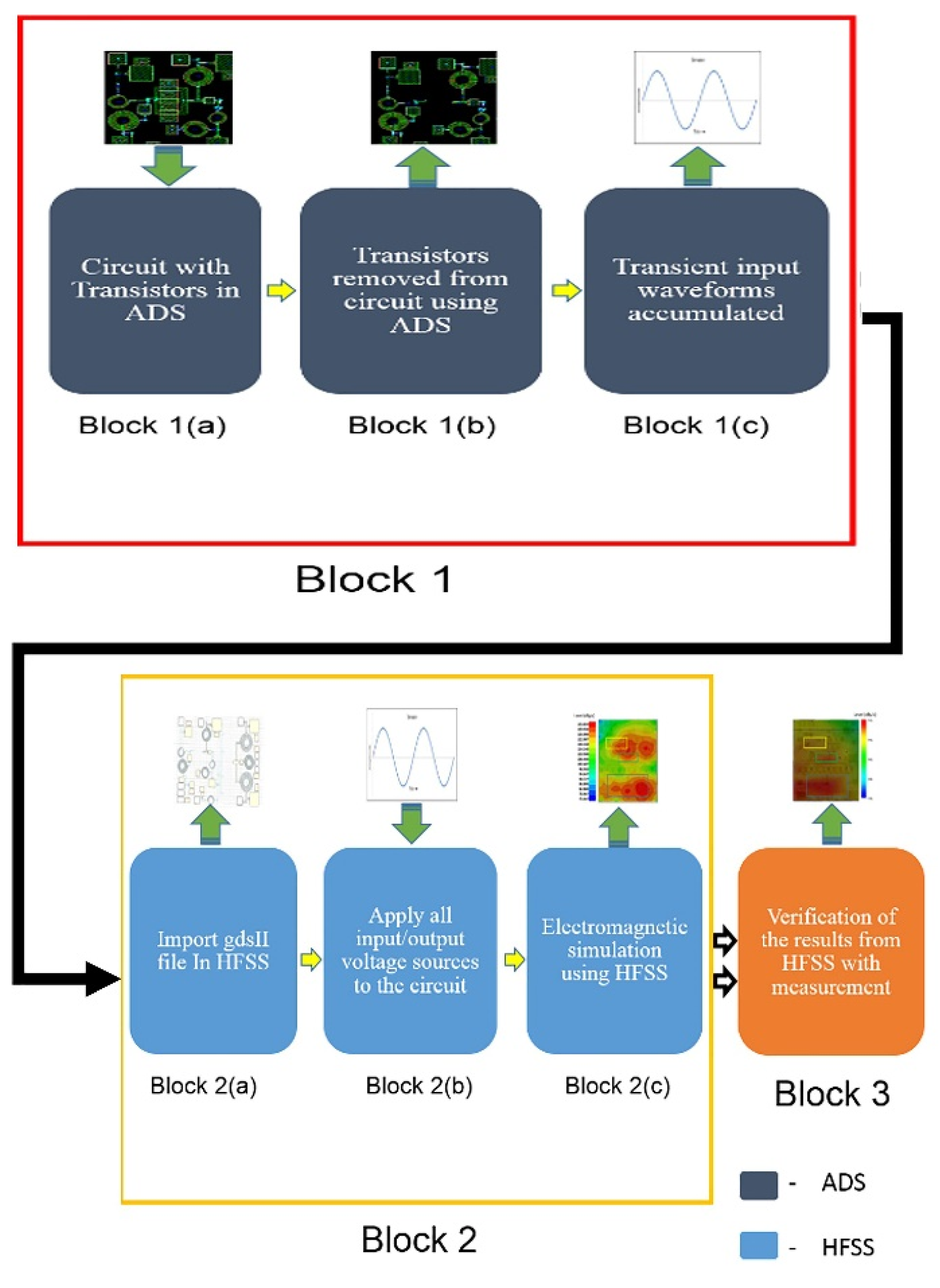
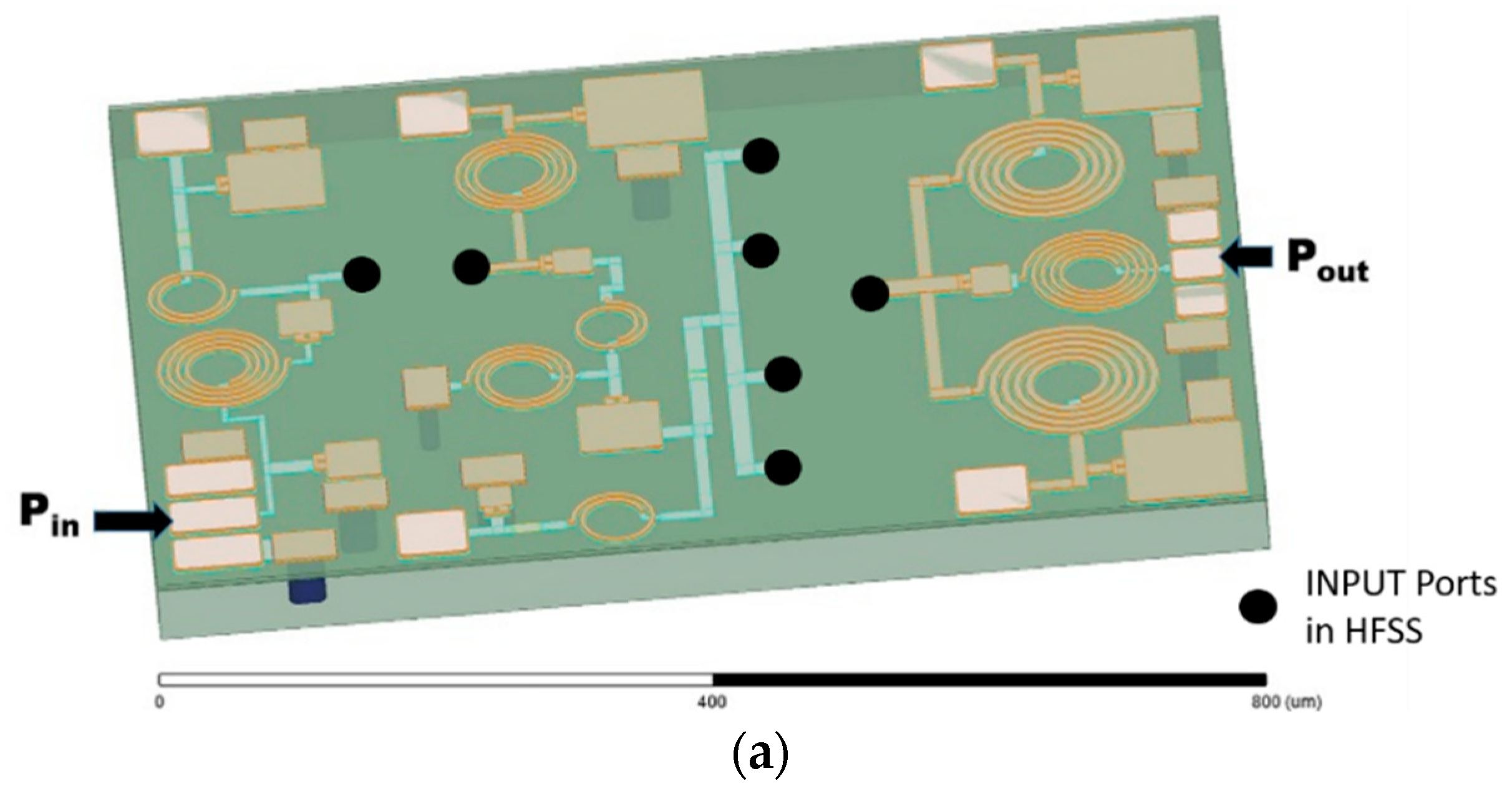
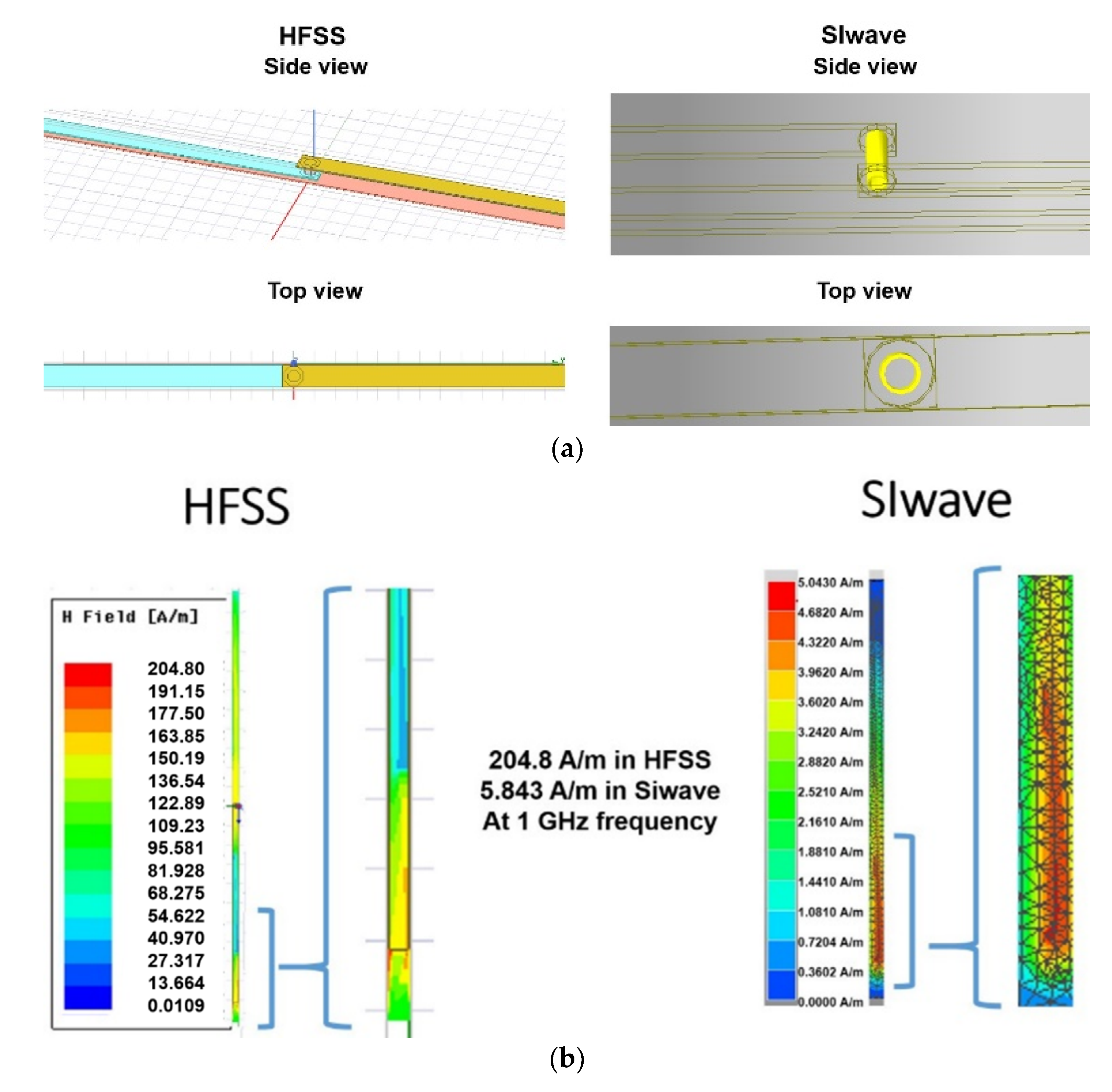
3. Simulation Methodology
- E(x,y,z) is a phasor representing an oscillating electric field;
- k0 is the free space wave number;
- , where ω is the angular frequency, which is 2πf;
- µr is the complex relative permeability;
- εr is the complex relative permittivity;
- S represents the radiation boundary surfaces;
- j is the imaginary unit ();
- ε0 is the relative permeability of the free space;
- Htan is the component of the magnetic field that is tangential to the surface;
- Enormal is the component of the electric field that is normal to the surface;
- Etan is the component of the electric field that is tangential to the surface;
- G is the free space Green’s function;
- J is the current density.
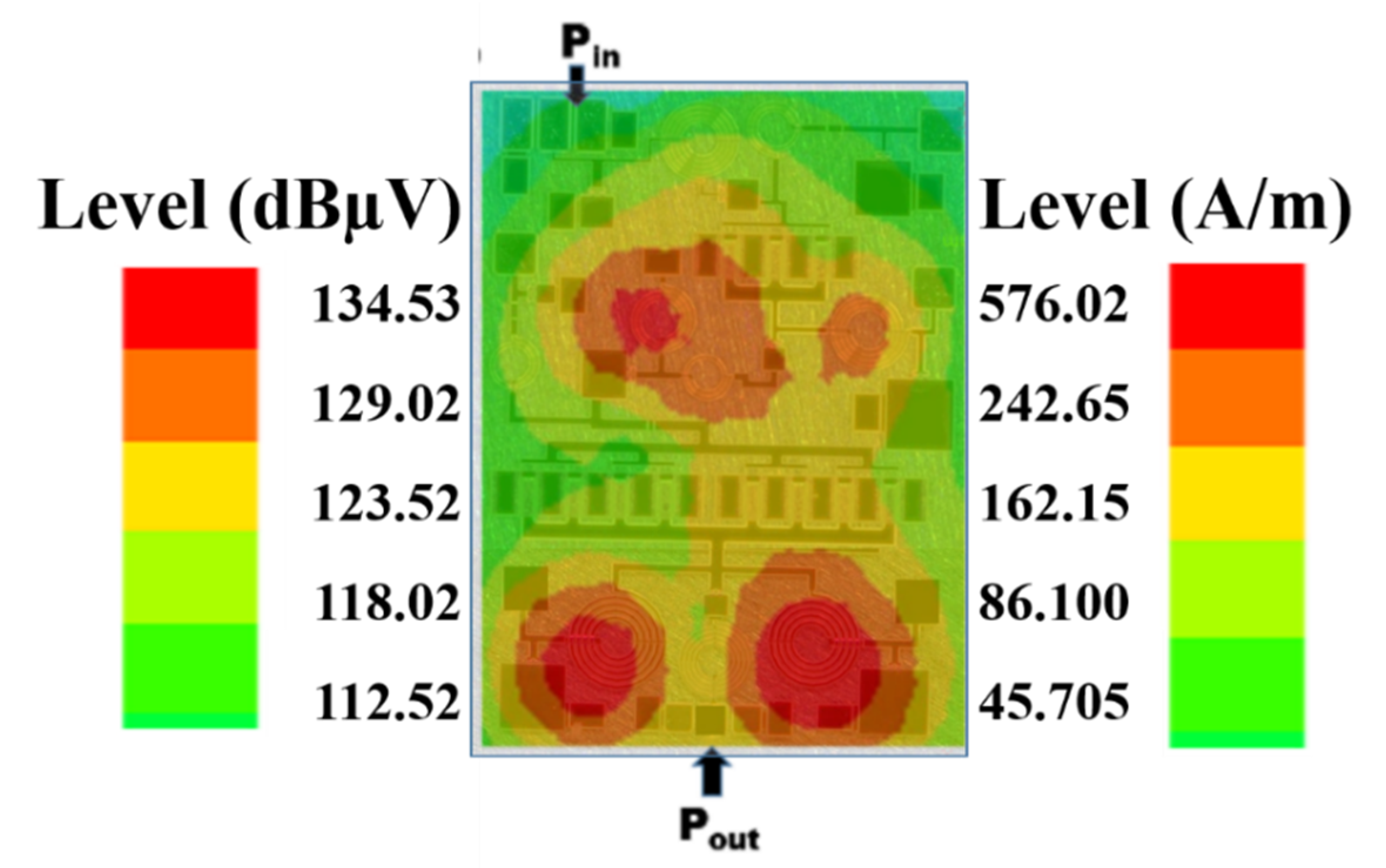
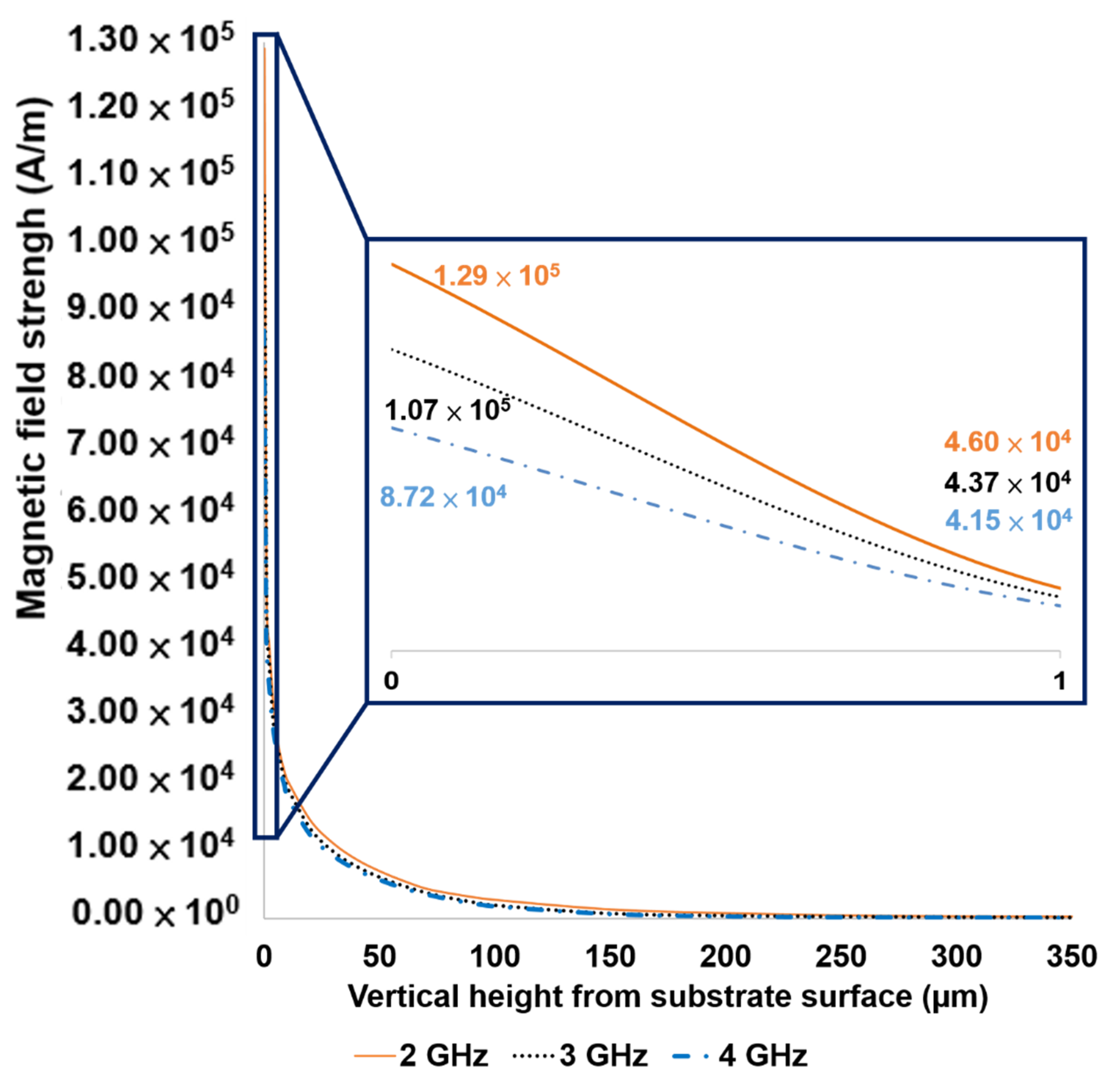
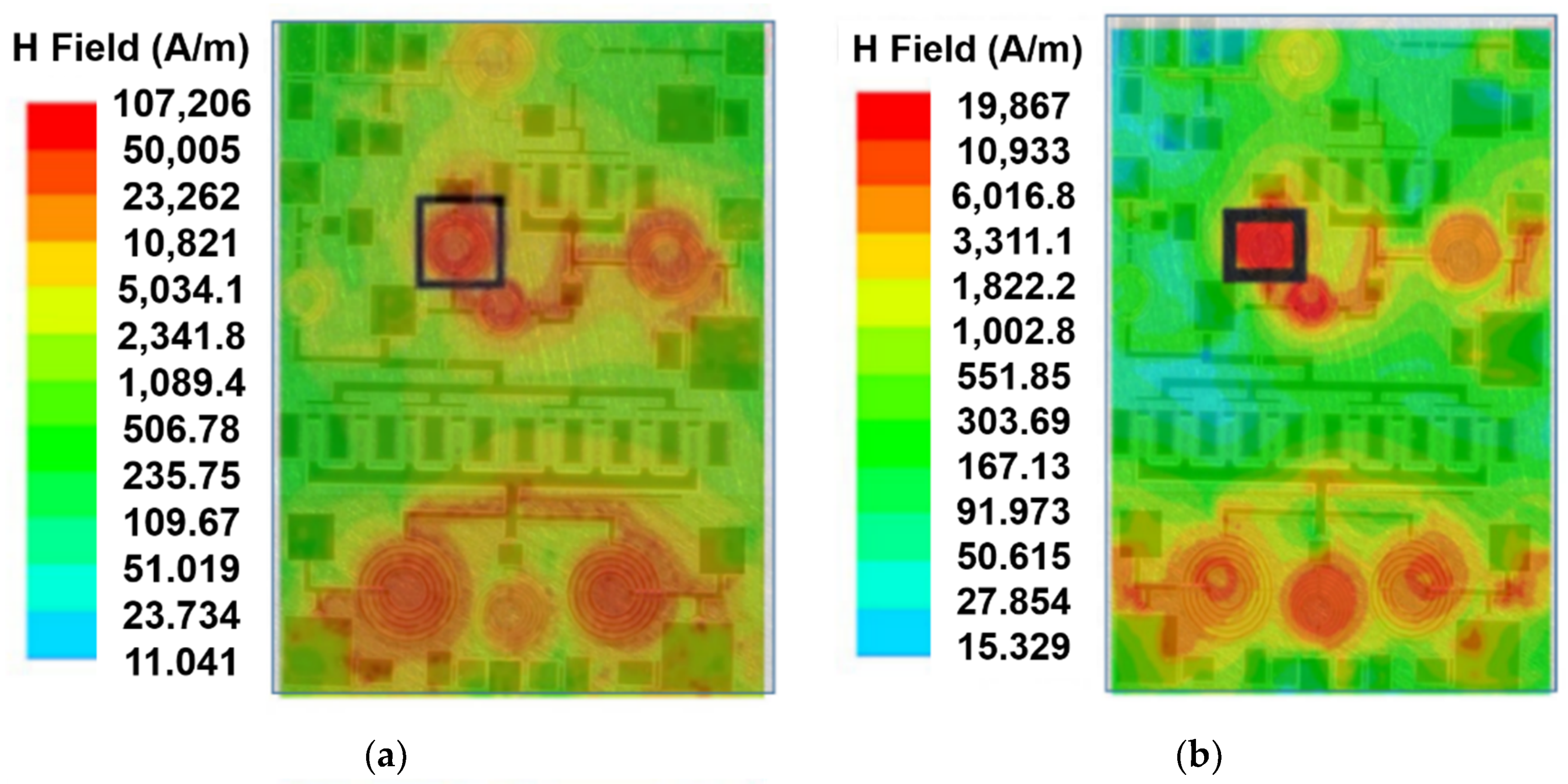
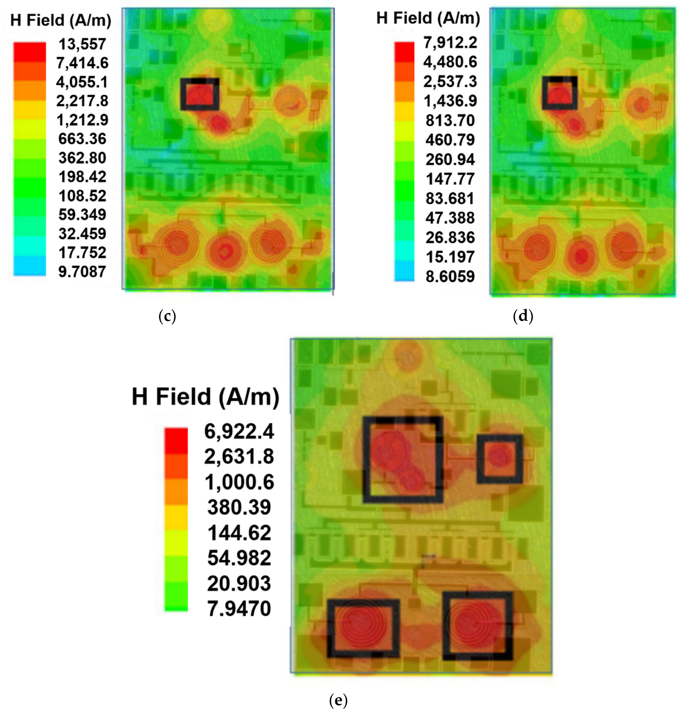
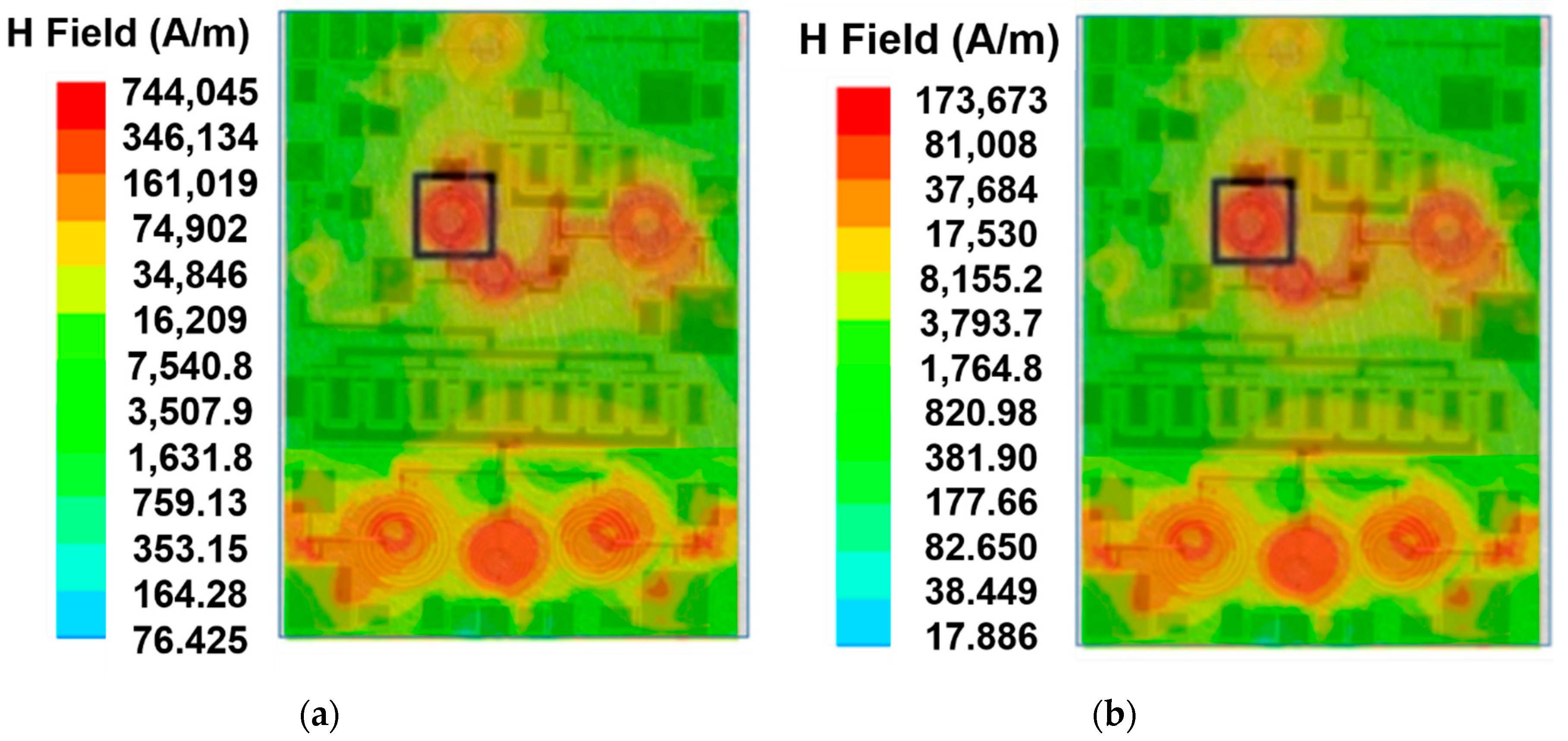
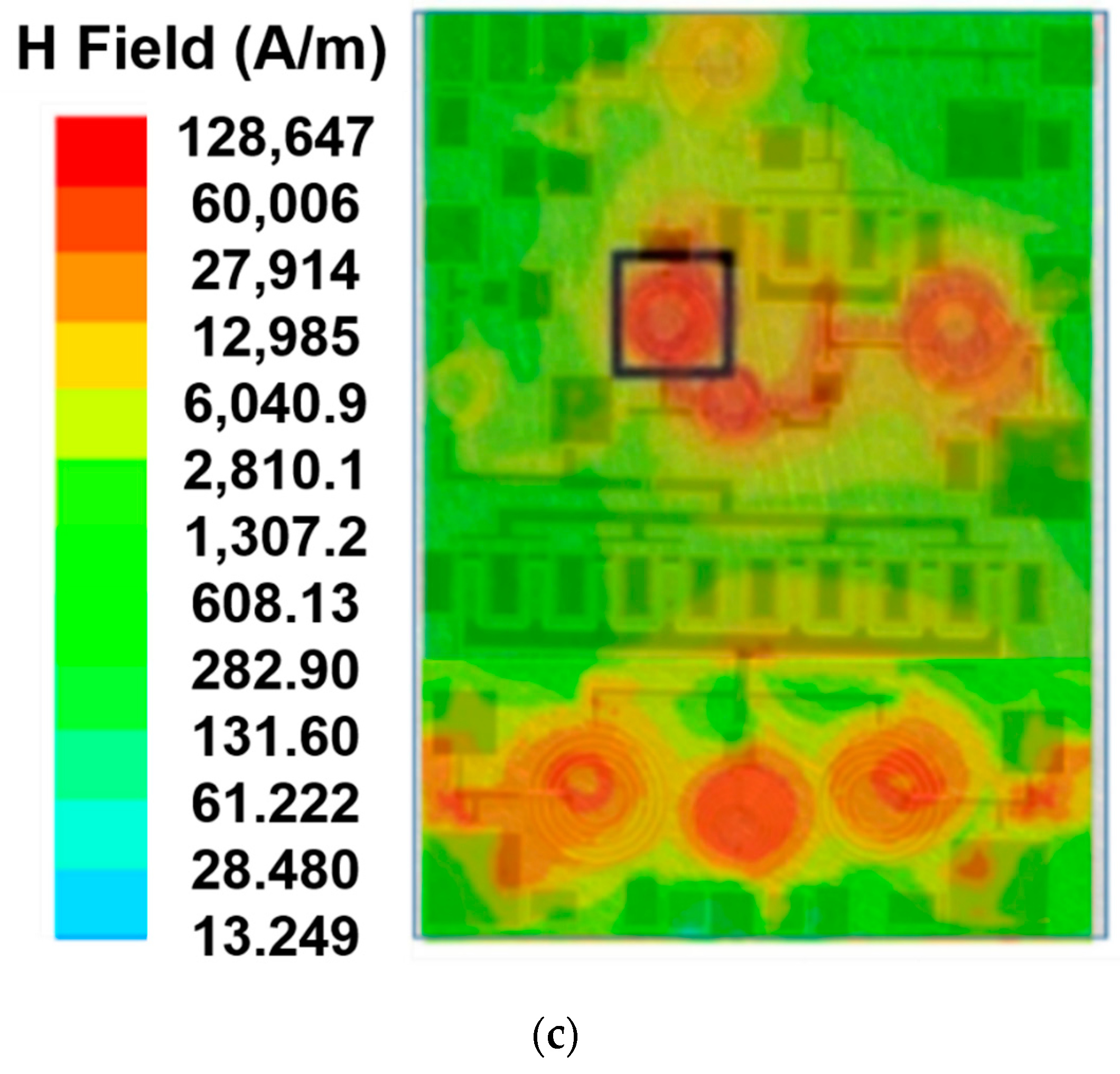
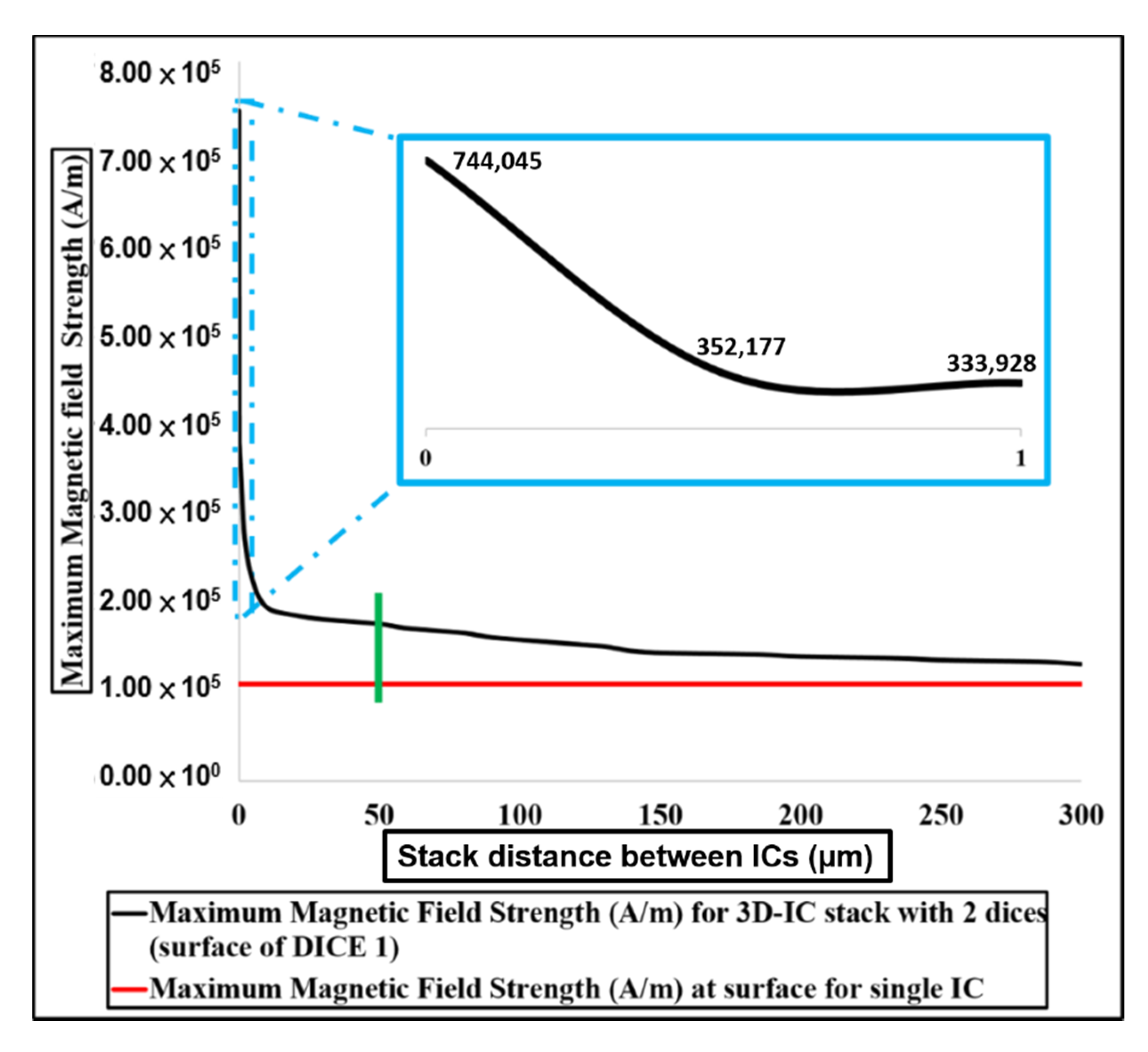
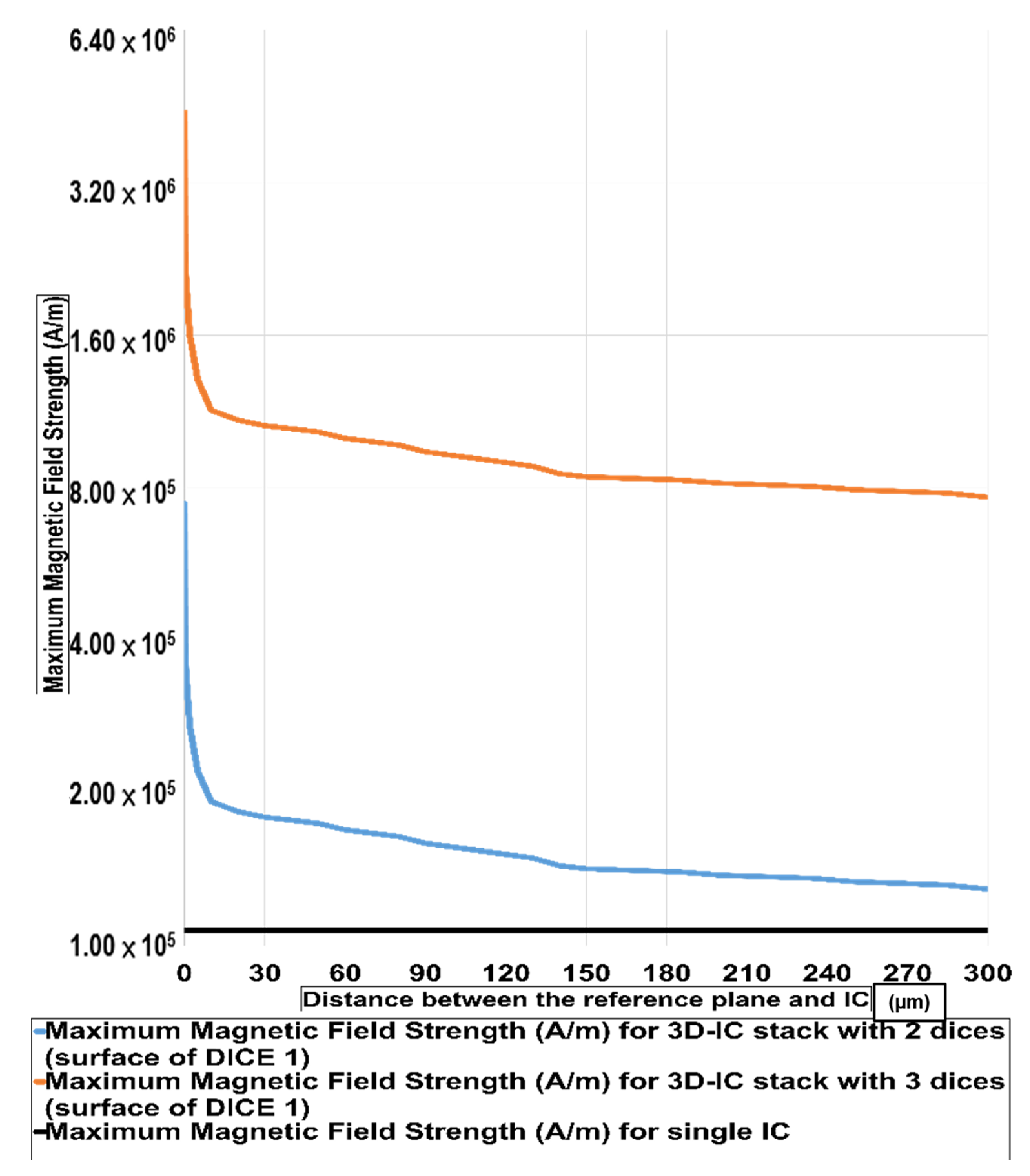
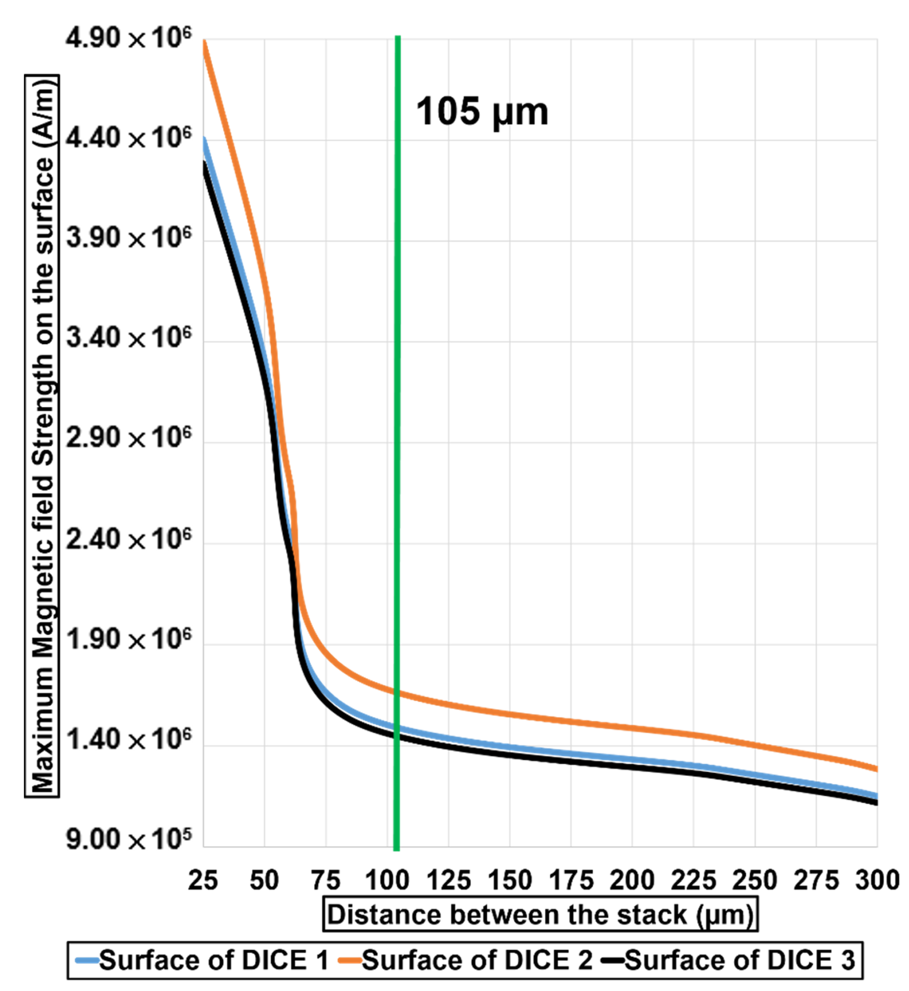
4. Electromagnetic Field Intensity Distribution
5. Conclusions
Author Contributions
Funding
Conflicts of Interest
References
- Zhan, C.J.; Juang, J.Y.; Lin, Y.M.; Huang, Y.W.; Kao, K.S.; Yang, T.F.; Lu, S.T.; Lau, J.H.; Chen, T.H.; Lo, R.; et al. Development of fluxless chip-on-wafer bonding process for 3DIC chip stacking with 30 μm pitch lead-free solder micro bumps and reliability characterization. In Proceedings of the 2011 IEEE 61st Electronic Components and Technology Conference (ECTC), Lake Buena Vista, FL, USA, 31 May–3 June 2011; pp. 14–21. [Google Scholar] [CrossRef]
- Knickerbocker, J.U.; Andry, P.S.; Dang, B.; Horton, R.R.; Interrante, M.J.; Patel, C.S.; Polastre, R.J.; Sakuma, K.; Sirdeshmukh, R.; Sprogis, E.J.; et al. Three—Dimensional silicon integration. IBM J. Res. Dev. 2008, 52, 553–569. [Google Scholar] [CrossRef]
- Dang, B.; Wright, S.L.; Andry, P.S.; Sprogis, E.J.; Tsang, C.K.; Interrante, M.J.; Webb, B.C.; Polastre, R.J.; Horton, R.R.; Patel, C.S.; et al. 3D chip stacking with C4 technology. IBM J. Res. Dev. 2008, 52, 599–609. [Google Scholar] [CrossRef]
- Emma, P.G.; Kursun, E. Is 3D chip technology the next growth engine for performance improvement? IBM J. Res. Dev. 2008, 52, 541–552. [Google Scholar] [CrossRef]
- Chaabouni, H.; Rousseau, M.; Leduc, P.; Farcy, A.; Thuaire, R.E.F.A.; Haury, G.; Valentian, A.; Billiot, G.; Assous, M.; de Crecy, F.; et al. Investigation on TSV impact on 65nm CMOS devices and circuits. In Proceedings of the 2010 International Electron Devices Meeting, San Francisco, CA, USA, 6–8 December 2010; pp. 796–799. [Google Scholar] [CrossRef]
- Cherman, V.O.; de Messemaeker, J.; Croes, K.; Dimcic, B.; van der Plas, G.; de Wolf, I.; Beyer, G.; Swinnen, B.; Beyne, E. Impact of through silicon vias on front-end-of-line performance after thermal cycling and thermal storage. In Proceedings of the 2012 IEEE International Reliability Physics Symposium (IRPS), Anaheim, CA, USA, 15–19 April 2012; pp. 5–9. [Google Scholar] [CrossRef]
- Beyne, E. Electrical, thermal and mechanical impact of 3D TSV and 3D stacking technology on advanced CMOS Devices-Technology directions. In Proceedings of the 2011 IEEE International 3D Systems Integration Conference (3DIC), Osaka, Japan, 31 January–2 February 2012. [Google Scholar] [CrossRef]
- Yahalom, G.; Ho, S.; Wang, A.; Ko, U.; Chandrakasan, A. Analog-Digital Partitioning and Coupling in 3D-IC for RF Applications. In Proceedings of the 2016 IEEE International 3D Systems Integration Conference (3DIC), San Francisco, CA, USA, 8–11 November 2016; pp. 1–4. [Google Scholar]
- Uemura, S.; Hiraoka, Y.; Kai, T.; Dosho, S. Isolation Techniques Against Substrate Noise Coupling Utilizing Through Silicon Via (TSV) Process for RF/Mixed Signal SoCs. IEEE J. Solid-State Circuits 2012, 47, 810–816. [Google Scholar] [CrossRef]
- Li, F.; Nicopoulos, C.; Richardson, T.; Xie, Y.; Narayanan, V.; Kandemir, M. Design and management of 3D chip multiprocessors using network-in-memory. Proc. Int. Symp. Comput. Archit. 2006, 2006, 130–141. [Google Scholar] [CrossRef]
- Loi, G.L.; Agrawal, B.; Srivastava, N.; Lin, S.C.L.S.C.; Sherwood, T.; Banerjee, K. A thermally-aware performance analysis of vertically integrated (3-D) processor-memory hierarchy. In Proceedings of the 43rd annual Design Automation Conference, San Francisco, CA, USA, 24–28 July 2016; pp. 991–996. [Google Scholar] [CrossRef]
- Mizunuma, H.; Yang, C.L.; Lu, Y.C. Thermal modeling for 3D-ICs with integrated microchannel cooling. In Proceedings of the 2009 International Conference on Computer-Aided Design, San Jose, CA, USA, 2–5 November 2009; pp. 256–263. [Google Scholar] [CrossRef]
- Koo, K.; Lee, S.; Kim, J. Vertical noise coupling on wideband low noise amplifier from on-chip switching-mode DC-DC converter in 3D-IC. In Proceedings of the IEEE Electromagnetic Compatibility of Integrated Circuits (EMC Compo), Dubrovnik, Croatia, 6–9 November 2011; pp. 35–40. [Google Scholar]
- Sicard, E.; Jianfei, W.; Shen, R.; Li, E.P.; Liu, E.X.; Kim, J.; Cho, J.; Swaminathan, M. Recent Advances in Electromagnetic Compatibility of 3D-ICs-Part II. IEEE Electromagn. Mag. 2016, 5, 65–74. [Google Scholar] [CrossRef]
- Sicard, E.; Jianfei, W.; Shen, R.J.; Li, E.P.; Liu, E.X.; Kim, J.; Cho, J.; Swaminathan, M. Recent advances in Electromagnetic Compatibility of 3D-ICs-Part I. IEEE Electromagn. Mag. 2015, 4, 79–89. [Google Scholar] [CrossRef]
- Agrawal, A.; Huang, S.; Gao, G.; Wang, L.; DeLaCruz, J.; Mirkarimi, L. Thermal and Electrical Performance of Direct Bond Interconnect Technology for 2.5D and 3D Integrated Circuits. In Proceedings of the 2017 IEEE 67th Electronic Components and Technology Conference (ECTC), Orlando, FL, USA, 30 May–2 June 2017; pp. 989–998. [Google Scholar] [CrossRef]
- Chen, S.; Tzeng, P.; Hsin, Y.; Wang, C.; Chang, P.; Chen, J.; Chen, T.; Hsu, T.; Chang, H.; Zhan, C.; et al. Implementation of Memory Stacking on Logic Controller by Using 3DIC 300mm Backside TSV Process Integration. In Proceedings of the 2016 International Symposium on VLSI Technology, Systems and Application (VLSI-TSA), Hsinchu, Taiwan, 25–27 April 2016; Volume 2, pp. 1–2. [Google Scholar] [CrossRef]
- Zhang, C.; Thadesar, P.; Zia, M.; Sarvey, T.; Bakir, M.S. Au-NiW mechanically flexible interconnects (MFIs) and TSV integration for 3D interconnects. In Proceedings of the 2014 International 3D Systems Integration Conference (3DIC), Kinsdale, Ireland, 1–3 December 2014; pp. 1–4. [Google Scholar] [CrossRef]
- Chen, J.C.; Chen, E.H.; Tzeng, P.J.; Lin, C.H.; Wang, C.C.; Chen, S.C.; Hsu, T.C.; Chen, C.C.; Hsin, Y.C.; Chang, P.C.; et al. Low-cost 3DIC process technologies for Wide-I/O memory cube. In Proceedings of the 2015 International Symposium on VLSI Technology, Systems and Applications, Hsinchu, Taiwan, 2–3 June 2015. [Google Scholar] [CrossRef]
- Yang, C.C.; Hsieh, T.Y.; Huang, W.H.; Wang, H.H.; Shen, C.H.; Shieh, J.M. Sequentially stacked 3DIC technology using green nanosecond laser crystallization and laser spike annealing technologies. In Proceedings of the 2015 IEEE 22nd International Symposium on the Physical and Failure Analysis of Integrated Circuits, Hsinchu, Taiwan, 29 June–2 July 2015; pp. 389–391. [Google Scholar] [CrossRef]
- Madhour, Y.; Zervas, M.; Schlottig, G.; Brunschwiler, T.; Leblebici, Y.; Thome, J.R.; Michel, B. Integration of intra chip stack fluidic cooling using thin-layer solder bonding. In Proceedings of the 2013 IEEE International 3D Systems Integration Conference (3DIC), San Francisco, CA, USA, 2–4 October 2013; pp. 1–8. [Google Scholar] [CrossRef]
- Ki, W.M.; Kang, M.S.; Yoo, S.; Lee, C.W. Fabrication and bonding process of fine pitch Cu pillar bump on thin Si chip for 3D stacking IC. In Proceedings of the 2011 IEEE International 3D Systems Integration Conference (3DIC), Osaka, Japan, 31 January–2 February 2012; pp. 3–6. [Google Scholar] [CrossRef]
- Kang, S.; Cho, S.; Yun, K.; Ji, S.; Bae, K.; Lee, W.; Kim, E.; Kim, J.; Cho, J.; Mun, H.; et al. TSV optimization for BEOL interconnection in logic process. In Proceedings of the 2011 IEEE International 3D Systems Integration Conference (3DIC), Saka, Japan, 31 January–2 February 2012. [Google Scholar] [CrossRef]
- Ahmad, H.; Izadi, O.H.; Shinde, S.; Pommerenke, D.; Shumiya, H.; Maeshima, J.; Araki, K. A study on correlation between near-field EMI scan and ESD susceptibility of ICs. In Proceedings of the IEEE International Symposium on Electromagnetic Compatibility Signal/Power Integrity, Washington, DC, USA, 7–11 August 2017; pp. 169–174. [Google Scholar] [CrossRef]
- Jin, S.; Cracraft, M.A.; Zhang, J.; DuBroff, R.E.; Slattery, K. Using near-field scanning to predict radiated fields. International Symposium on Electromagnetic Compatibility. In Proceedings of the 2004 International Symposium on Electromagnetic Compatibility (IEEE Cat. No.04CH37559), Silicon Valley, CA, USA, 9–13 August 2004; Volume 1, pp. 14–18. [Google Scholar] [CrossRef]
- Yu, Z.; Koo, J.; Mix, J.A.; Slattery, K.; Fan, J. Extracting physical IC models using near-field scanning. In Proceedings of the IEEE International Symposium on Electromagnetic Compatibility, Fort Lauderdale, FL, USA, 25–30 July 2010; pp. 317–320. [Google Scholar] [CrossRef]
- Slattery, K.P. A comparison of the near field and far field emissions of a Pentium (R) clock IC. In Proceedings of the IEEE EMC International Symposium. Symposium Record. International Symposium on Electromagnetic Compatibility, Montreal, QC, Canada, 13–17 August 2001; Volume 1, pp. 547–551. [Google Scholar] [CrossRef]
- Xiaopeng, D.; Deng, S.; Hubing, T.; Beetner, D. Analysis of chip-level EMI using near-field magnetic scanning. In Proceedings of the International Symposium on Electromagnetic Compatibility, Silicon Valley, CA, USA, 9–13 August 2004; Volume 1, pp. 174–177. [Google Scholar] [CrossRef]
- Stefanini, I.; Markovic, M.; Perriard, Y. 3D Inductance and Impedance Determination Taking Skin Effect into Account. In Proceedings of the IEEE International Conference on Electric Machines and Drives, San Antonio, TX, USA, 15 May 2005; Volume 2, pp. 74–79. [Google Scholar] [CrossRef]
- Lau, J.H.; Yue, T.G. Thermal management of 3D IC integration with TSV (through silicon via). In Proceedings of the 2009 59th Electronic Components and Technology Conference, San Diego, CA, USA, 26–29 May 2009; pp. 635–640. [Google Scholar]
- Patrick, L.; de Crecy, F.; Fayolle, M.; Charlet, B.; Enot, T.; Zussy, M.; Jones, B.; Barbe, J.C.; Kernevez, N.; Sillon, N.; et al. Challenges for 3D IC integration: Bonding quality and thermal management. In Proceedings of the 2007 IEEE International Interconnect Technology Conferencee, Burlingame, CA, USA, 4–6 June 2007; pp. 210–212. [Google Scholar]
- Kiran, P.; Loh, G.H. Thermal analysis of a 3D die-stacked high-performance microprocessor. In Proceedings of the 16th ACM Great Lakes Symposium on VLSI, Providence, RI, USA, 16–18 May 2010; pp. 19–24. [Google Scholar]
- Lau John, H.; Yue, T.G. Effects of TSVs (through-silicon vias) on thermal performances of 3D IC integration system-in-package (SiP). Microelectron. Reliab. 2012, 52, 2660–2669. [Google Scholar]
- Sangwan, V.; Kapoor, D.; Tan, C.M.; Lin, C.H.; Chiu, H.C. High Frequency Electromagnetic Simulation and Optimization for GaN-HEMT Power Amplifier IC. IEEE Trans. Electromagn. Compat. 2018, 61, 564–571. [Google Scholar] [CrossRef]
- Ansys Inc. Ansys HFSS Technical Notes; ANSYS: Canonsburg, PA, USA, 2017. [Google Scholar]
- Ott, H.W. Electromagnetic Compatibility Engineering; John Wiley Sons: Hoboken, NJ, USA, 2009. [Google Scholar]


© 2020 by the authors. Licensee MDPI, Basel, Switzerland. This article is an open access article distributed under the terms and conditions of the Creative Commons Attribution (CC BY) license (http://creativecommons.org/licenses/by/4.0/).
Share and Cite
Kapoor, D.; Tan, C.M.; Sangwan, V. Evaluation of the Potential Electromagnetic Interference in Vertically Stacked 3D Integrated Circuits. Appl. Sci. 2020, 10, 748. https://doi.org/10.3390/app10030748
Kapoor D, Tan CM, Sangwan V. Evaluation of the Potential Electromagnetic Interference in Vertically Stacked 3D Integrated Circuits. Applied Sciences. 2020; 10(3):748. https://doi.org/10.3390/app10030748
Chicago/Turabian StyleKapoor, Dipesh, Cher Ming Tan, and Vivek Sangwan. 2020. "Evaluation of the Potential Electromagnetic Interference in Vertically Stacked 3D Integrated Circuits" Applied Sciences 10, no. 3: 748. https://doi.org/10.3390/app10030748
APA StyleKapoor, D., Tan, C. M., & Sangwan, V. (2020). Evaluation of the Potential Electromagnetic Interference in Vertically Stacked 3D Integrated Circuits. Applied Sciences, 10(3), 748. https://doi.org/10.3390/app10030748