1. Introduction
Currently, the development of various materials (of high-strength, lightweight, etc.) is proceeding at a high rate in various industries and it is important to know their exact electrophysical parameters. Thus, the study of the electrophysical parameters of the obtained materials is an urgent task.
To study the electrophysical parameters of materials, waveguide [
1], coaxial [
2,
3,
4,
5,
6,
7,
8,
9,
10], as well as methods based on the use of horn antennas [
11] are usually used.
Waveguide methods are based on the use of rectangular waveguides. The work conducted in [
12] presents an installation in the form of a measuring two-ridge waveguide. The use of this setup allowed the authors to expand the frequency range (7.5–18 GHz) due to the localization of energy between two protrusions. The results obtained for three measured samples with different values of the real part of the permittivity have an error of 2%, 3.3%, and 4.7%. With an increase in the value of the real part of permittivity
, the measurement error increases. It subsequently can adversely affect the measurement of strongly absorbing media.
Waveguide methods (or open waveguide methods) also have two approaches: Using one or two ports. The one-port wave method [
13,
14,
15,
16,
17,
18,
19,
20,
21] usually consists of several measurements with a change in the thickness of the air gap between the waveguide and test sample. These methods are also measuring the reflected signal when there is air behind the test sample and measure the transmitted signal if the metal is located behind the test sample [
4]. The two-port waveguide measurement method uses two sources of electromagnetic waves. This approach allows measurements in a wide frequency band but has a number of limitations that do not allow obtaining data with high accuracy, since there is an air gap between the sample under study and the wide wall of the waveguide. When measuring, the presence of this gap leads to a sharp jump in the electric field strength at the “air-material” transition [
22].
Coaxial methods are based on the use of a measuring transmission line. Among the coaxial methods, we can mention the setup proposed in [
12]. Here, measurements are taken by filling the entire inner space of the cell. This method is the most accurate, but it is necessary that the measuring line passes through the entire test sample. In this experiment, there may be air gaps around the perimeter of the sample, and the imperfect surface of the walls of the transmission line may introduce errors in measurements, which must also be taken into account when obtaining data.
The method of studying the dielectric and magnetic permeability using two horn antennas has its advantages, since it can be used in free space. Thus, in [
23], an installation is presented using two horn antennas aimed at the material under study. To exclude unwanted reflection from the environment, the setup was located in an anechoic chamber. The measurements were carried out in the frequency range 8–12 GHz. In [
24], additional focusing lenses are used to eliminate lateral radiation. The focus of the two antennas is located directly inside the material under study, which makes it possible to determine the electrophysical parameters with high accuracy, as well as carry out measurements outside the anechoic chamber. The authors declare that they managed to achieve an accuracy of 2% when measuring the real part of the dielectric permittivity.
Many of the methods discussed are implemented in installations of companies such as SPEAG and Keysight technologies. These installations, in particular the line of SPEAG Dielectric Assessment Kit (DAK) systems, namely the DAK-TL2, make measurements only by the contact method, that is, the emitter must be directly adjacent to the sample under study. Measurements are carried out in a wide frequency range from 5 to 67 GHz (for the DAK-1.2E-TL2 installation). Wherein the area and thickness of the sample should not exceed certain dimensions. In particular, it is said about the thickness of the material that it should not exceed more than 10 mm. There are no clear references to specific sizes in open sources. However, it is clear that the setup was designed to study small samples. It is easier to create and produce the research material itself. In this case, an industrial batch quality control approach probably requires dedicated time to process the material or create a separate probe for each batch.
SPEAG also has DAK series rigs, which consist of three separate probes (DAK 12, DAK 3.5, and DAK 1.2E) that cover the frequency range from 4 to 67 GHz. This series of installations is distinguished by the fact that, using coaxial probes, it allows you to quickly and easily measure liquids. But the measurement of solid materials takes place by applying probes close to each other. In addition, a plane and smooth surface is also important for this installation.
The Keysight Technologies measurement setup allows measurements in the range from 18 to 110 GHz. At the same time, it uses two horn antennas to measure the dielectric properties of materials, which means that a vector analyzer is required for use. This significantly increases the cost of this technology. Each of the horn antennas of the installation is equipped with lenses made of a dielectric material with frequency dispersion. This indicates a less accurate measurement of samples. Additionally, this setup only measures plane and smooth samples.
As the analysis of existing methods and implemented installations shows, each has its own disadvantages: The precision of installations, the duration of measurements, complex mechanics, and expensive positioning systems with various drives for measurement accuracy, sensitivity to lateral radiation and the influence of external radiation, the requirement for measurements in an anechoic chamber, or the use of absorbers.
Thus, the problem of creating a method for measuring the electrophysical parameters of materials that is easier to operate, less demanding on various factors, and ensures a sufficient measurement accuracy remains relevant.
In this paper, it is proposed to relate the measured reflected signals at different frequencies with the electrophysical parameters of the measured materials on the basis of the well-known mathematical apparatus developed for the reflection of plane waves [
25]. It is proposed to use a collimated beam obtained by focusing the probe radiation on the surface of the material under study to form a plane wave in the measurement area. The parabolic metal mirror was used for focusing, which significantly reduces the frequency dispersion. This method is new and has not been previously noticed in the literature. The proposed approach was tested on a laboratory setup developed by the authors and presented in the article.
2. Methods
To find out the electrophysical parameters of materials, a technique was chosen that is a combination of the approaches considered in the literature based on measuring the reflected and transmitted signals. Finding the reflected signal is carried out due to the location of the material in the focus of electromagnetic waves. The transmitted signal is determined by placing a metal plate over the material under study. This approach can significantly simplify measurements. The use of a small-sized directional antenna makes it possible to reduce its secondary radiation to the sample. Before the study, it is necessary to measure the background signal to eliminate possible extraneous reflections of the probing signal in the absence of the test material. Further actions of the chosen technique are based on mathematical transformations.
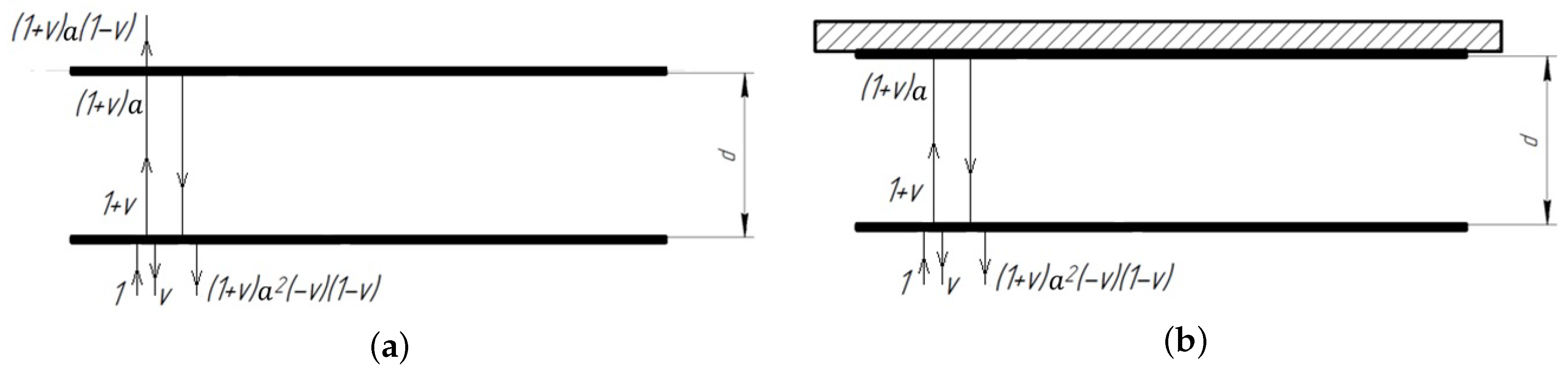
One of the important components in finding out electrophysical parameters is taking into account multiple reflections. Thus, it is necessary to take into account the three components “air-dielectric”, “air-dielectric-air”, and “air-dielectric-metal”.
To calculate the field after passing through the dielectric layer and reflected from the metal plate, a theoretical calculation of the reflection coefficient was performed. The coefficient of reflection from the «air-dielectric» half-spaces interface has the form:
where,
is the wave impedance,
is the refractive index of a medium,
, and
is the relative electric permittivity and magnetic permeability of the surrounding medium. All parameters have a dependence on the radiation frequency and therefore, are considered as functions of the frequency
.
When considering the case when the reflection from the «air-dielectric-air» interface is calculated (
Figure 1a), the complex amplitude has the form:
where,
.
In this case, the field strength reflection coefficient is:
. Substituting Formula (
2) in this expression, we obtain complex reflection coefficient in terms of field strength:
where,
d is the material thickness and
k is the wave number.
For the case when the “air-dielectric-metal” reflection is calculated (
Figure 1b), the complex amplitude has the form:
In this case, the field strength transmission coefficient is:
. Substituting the Equation (
4) in this expression, we obtain the complex reflection coefficient for the field strength:
To search for the refractive index
, it is necessary to solve the system of equations for
and
:
Solving this system of equations, we find out the value
for the relative dielectric permittivity and
for the relative magnetic permeability.
where,
.
The developed original solution will be applicable for measuring dielectric samples and absorbers. Unlike existing methods, this solution is used with a single source of electromagnetic waves and a parabolic reflector. This approach can greatly simplify measurements. The laboratory model was created to implement this method and is described below.
Furthermore, the results of measurements, their processing, and analysis of the results will be presented.
3. Experiments
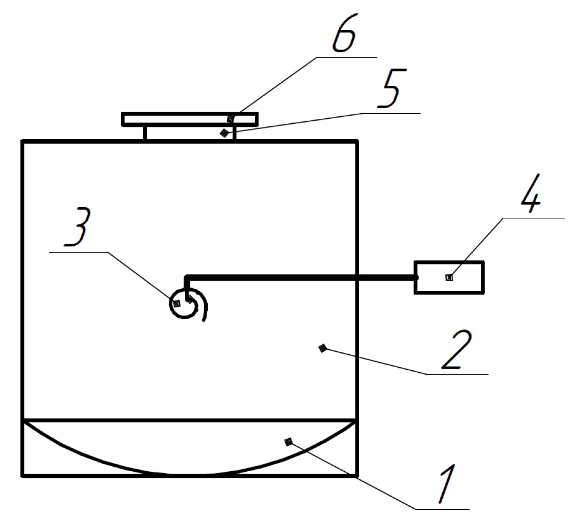
The proposed laboratory model consists of several components (
Figure 2): A broadband antenna and parabolic mirror. As a parabolic mirror, it is proposed to use a round elliptical reflector—a parabolic reflector antenna that can provide a plane front. The mirror profile is the surface of a paraboloid of revolution resulting from the rotation of the parabola. To provide a collimated beam in the measurement plane, it is necessary to move the antenna out of focus of the paraboloid. The 3D model of this system was made in the CST Microwave Studio program to find the optimal geometric parameters of the installation.
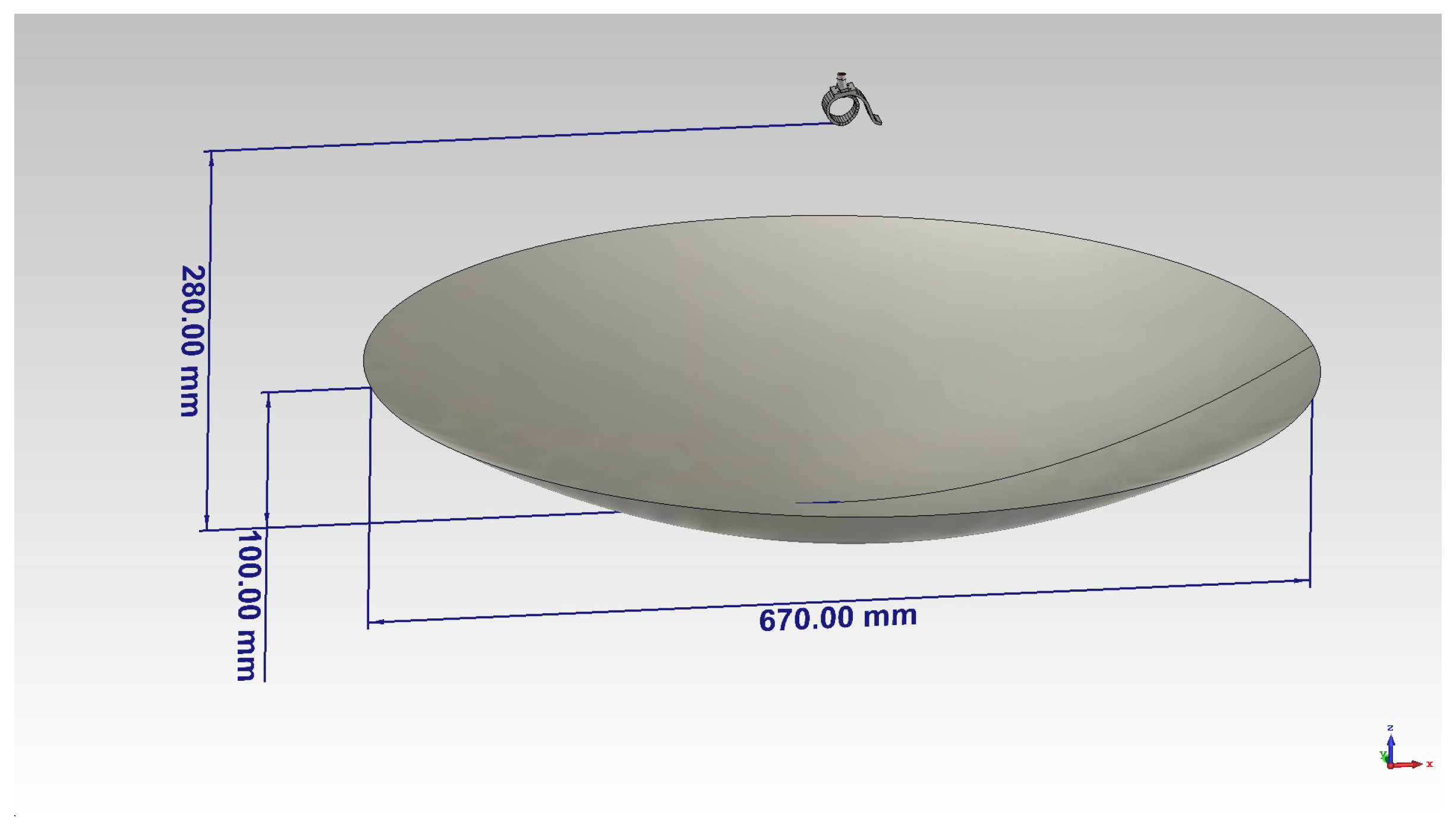
Before modeling, a calculation for an elliptical reflector was carried out. A reflector is one of the main components of the laboratory model. For the calculation, we used the law of equality of optical path lengths between fronts and the parabolic equation. The required dimensions of the reflector were obtained as follows: The diameter was 670 mm, the depth was 100 mm, the opening angle was 73, and the focal length was 280 mm.
Next, the model of a focusing system was built for measuring the electrophysical properties of materials (
Figure 3) using the CST Microwave Studio software.
The combined ultra-wideband (UWB) antenna with a low standing wave ratio in a wide range was selected as an emitter (
Figure 3). The antenna is located at a distance of 280 mm from the lower boundary of the reflector as it was obtained from mathematical calculations. This distance for the calculated parabolic mirror (reflectometer) provides a focus of radiation with a minimum spot diameter.
Based on the simulation results, the field distribution in the frequency range 3–13 GHz was obtained (
Figure 4). This range is selected based on the minimum voltage standing wave ratio (VSWR) value. The collimated beam is focused at a distance of 680 mm from the reflector. The size of the beam diameter varies in the range of 110–130 mm.
The laboratory model was made for the experimental study. The size and location of the elements in it are identical to what was intended in the CST Microwave Studio program.
The laboratory model (UWB measuring complex) was made from expanded polystyrene in the form of a parallelepiped with a height of one meter (
Figure 5). A UWB antenna and a focusing parabolic mirror (reflectometer) were placed inside it. The measuring complex also contains a vector reflectometer. An ultra-wideband feed antenna is connected to the vector reflectometer port, which is located at the first focus of the elliptical reflector. The second focus of the elliptical reflector is located on the upper boundary of the installation, made of expanded polystyrene. This approach to the measurement provides the necessary condition for measuring the reflection coefficient and the incidence of a plane wave on the object under study with a front parallel to the plane of the sample. The plane of measurement of the sample is perpendicular to the focal axis of the elliptical mirror.
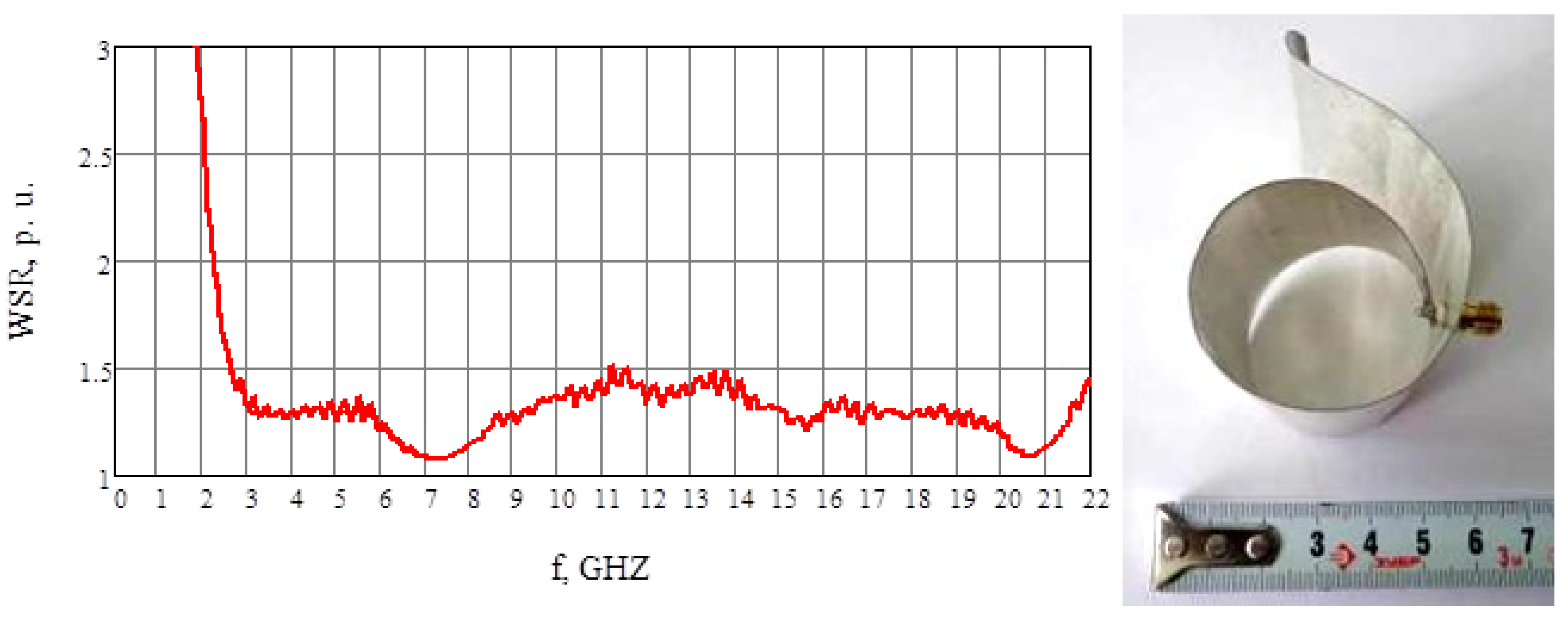
We used the ultra-wideband combined ultra-wideband (UWB) antenna of the “Snail” type which represents combination of an electric and a magnetic feed. This design allows the antenna bandwidth to be expanded towards low frequencies and reduced in size (
Figure 6). With rather small dimensions of 50 × 40 × 40 mm, the antenna was matched in the 1.2–18 GHz frequency band. This made it possible to emit and receive ultra-wideband electromagnetic pulses with a duration of 0.15 to 0.5 ns with little distortion.
Figure 6 on the left shows the frequency dependence of the standing wave ratio (VSWR) for radiation sources. It can be seen that the operating frequency band is in the range from 3 to 20 GHz.
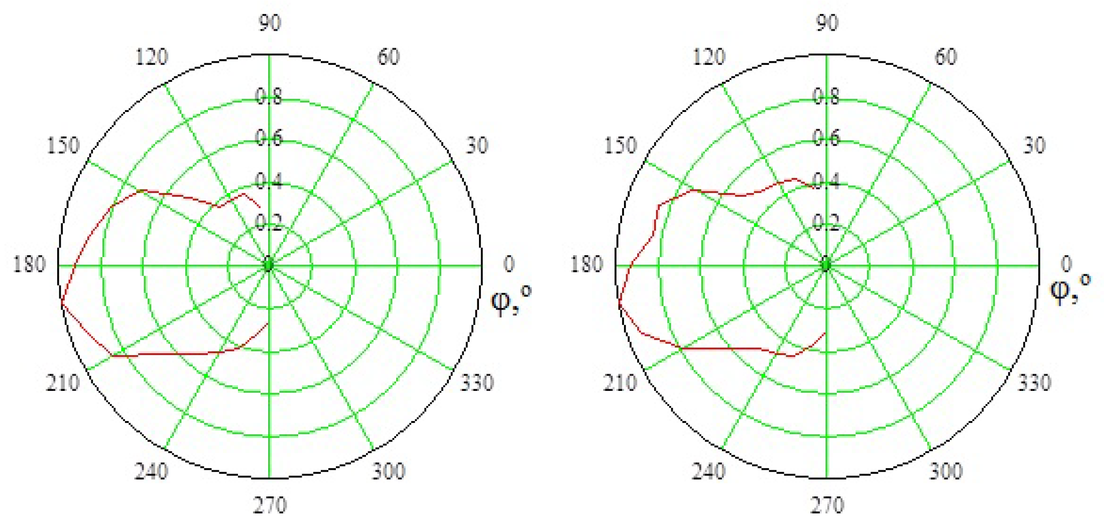
The radiation pattern for the peak field strength when a bipolar voltage pulse is applied to the antenna input is shown in
Figure 7.
The directional pattern (DP) of the radiator in the horizontal plane is symmetric and amounts about 90
at the level of 0.7. In the vertical plane, the pattern is tilted due to the asymmetrical shape of the antenna (
Figure 7).
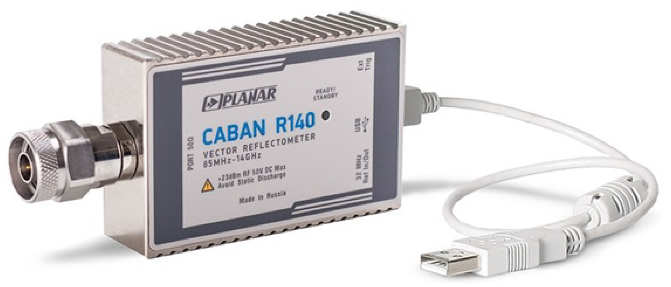
A CABAN R140 was used as a vector reflectometer (
Figure 8). It is intended for measuring the complex reflectivity of multipoles. This device is used during the testing, tuning, and development of various antenna feeder devices (AFD). The CABAN R140 device can be used in field conditions, in industrial production, in laboratories, as well as a part of automated measuring instruments and stands. In addition, this vector reflectometer allows remote control in accordance with COM/DCOM software technology.
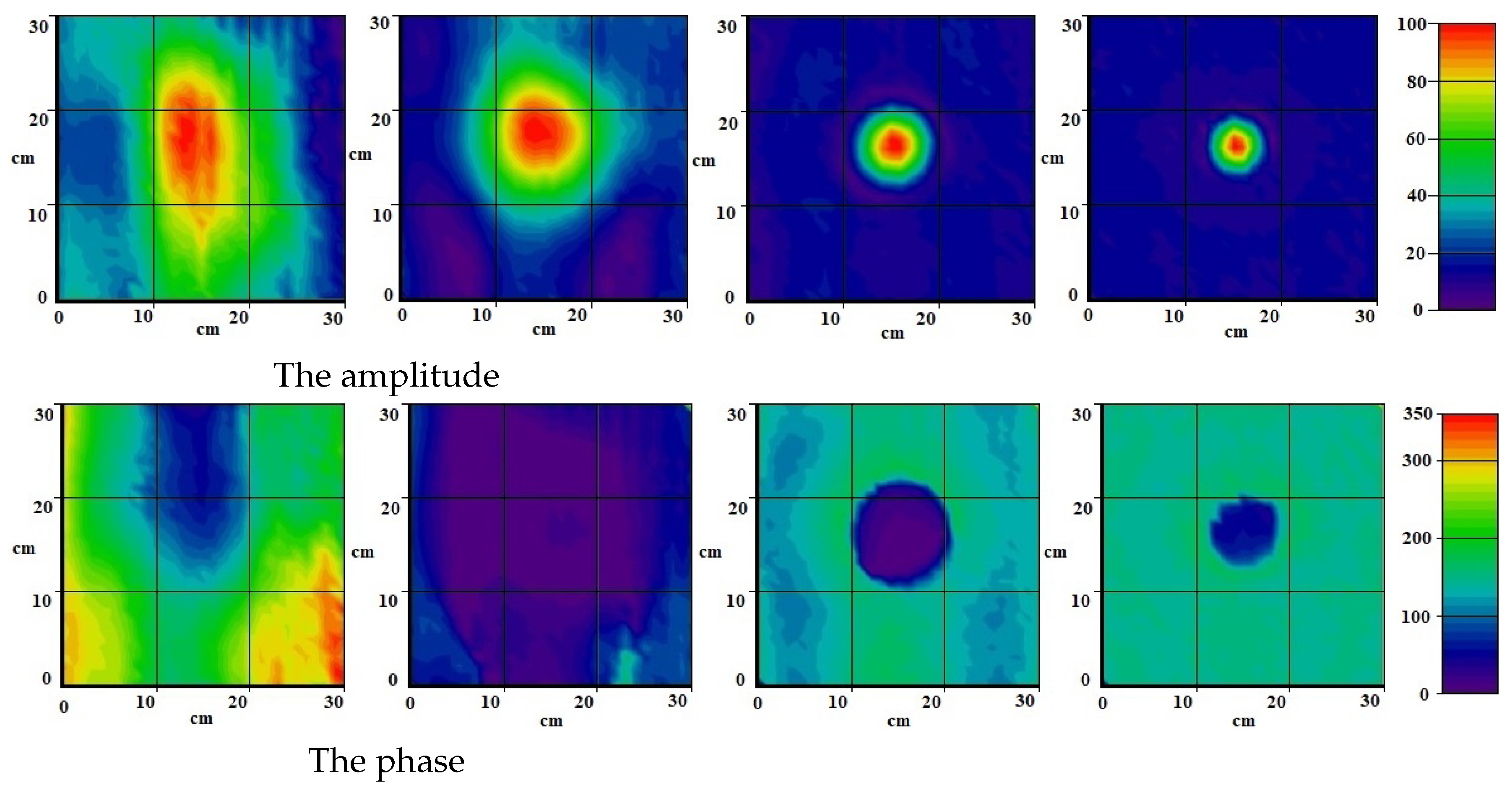
Before conducting experimental studies, the amplitude and phase of the field on the surface of the laboratory model were measured (
Figure 9). To obtain reliable data on materials, it is necessary to ensure the incidence of a plane wave on the material under study—a collimated beam with a uniform phase. As can be seen from the graphs presented in
Figure 9, starting from 3 GHz, clear focusing of the amplitude and phase uniformity in the focusing area are visible, on the basis of which it can be concluded that a plane wave is obtained in the measurement area. Analysis of the obtained results showed that the operating frequency range is 3–13 GHz. In
Figure 9, the dimensions in centimeters are plotted along the axes, one division is 10 cm. The size of the focusing area varies in the range 170–80 mm with increasing frequency and the size of the collimated beam decreases.
The analysis of the obtained results of measuring the amplitude and phase showed that the dimensions of the sample for research should be at least 150 × 150 mm.
In the experimental measurement procedure, the background signal was first measured in the absence of the measured sample. Furthermore, a metal plate was placed on the upper boundary of the measuring complex, and the measurement was carried out. After that, a sample to be measured was placed on the surface of the laboratory model (complex) and one more measurement was carried out. At the last stage, a metal plate was placed on top of the measured material sample. In the first case, a metal plate is used to detect the start of the signal, in the second case, to measure a passing signal (S12). Reflection is measured without a metal plate.
4. Results
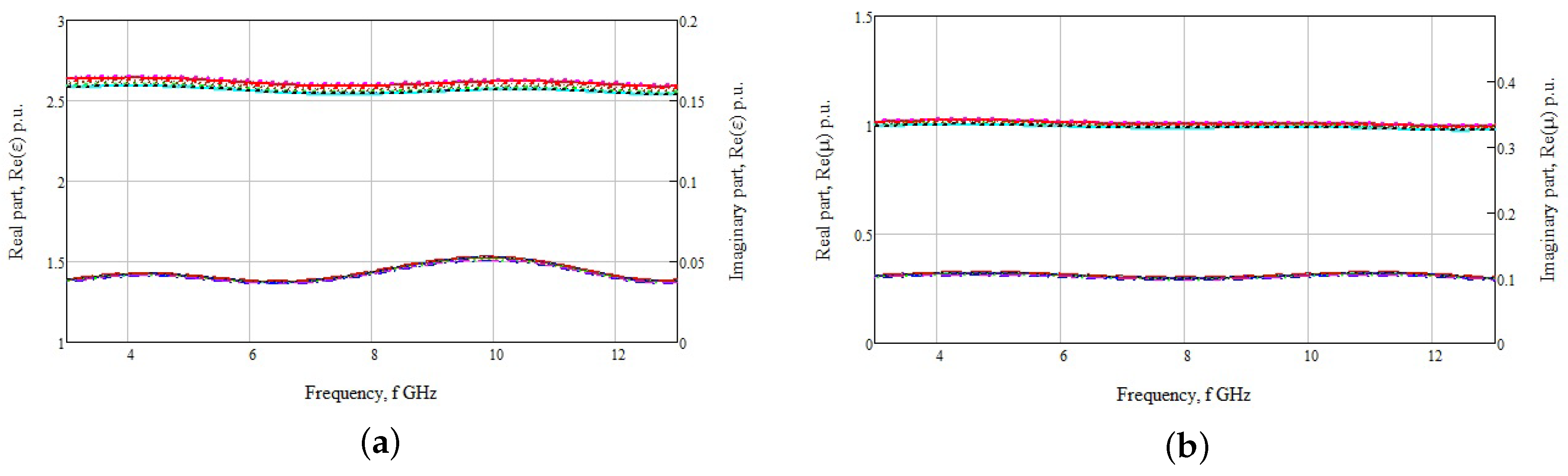
Measurements were carried out on two samples of material with known values of dielectric permittivity and magnetic permeability to confirm the reliability and estimate the accuracy of the created laboratory model (UWB measuring complex) and the developed method.
Plexiglas sheet with a thickness of 14.1 mm was chosen as the first known sample. Measured values of the complex dielectric permittivity and magnetic permeability obtained for it are presented below (
Figure 10). In the graphs below and subsequent ones, two ordinate axes are used. On the left are the values of the real part of both dielectric permittivity and magnetic permeability. On the right are the values of the imaginary part of the corresponding permeabilities. The reference value of the real part of the dielectric permittivity for plexiglas is
= 2.6 [
26]. To check the repeatability, 100 measurements were taken. Due to the fact that the Mathcad program does not allow placing more than 16 curves on the graphs, eight curves were taken from the real part of both the magnetic permeability and the dielectric permittivity. Eight curves were taken for the imaginary parts of the magnetic permeability and dielectric permittivity.
The average value of the real part of the dielectric permittivity was
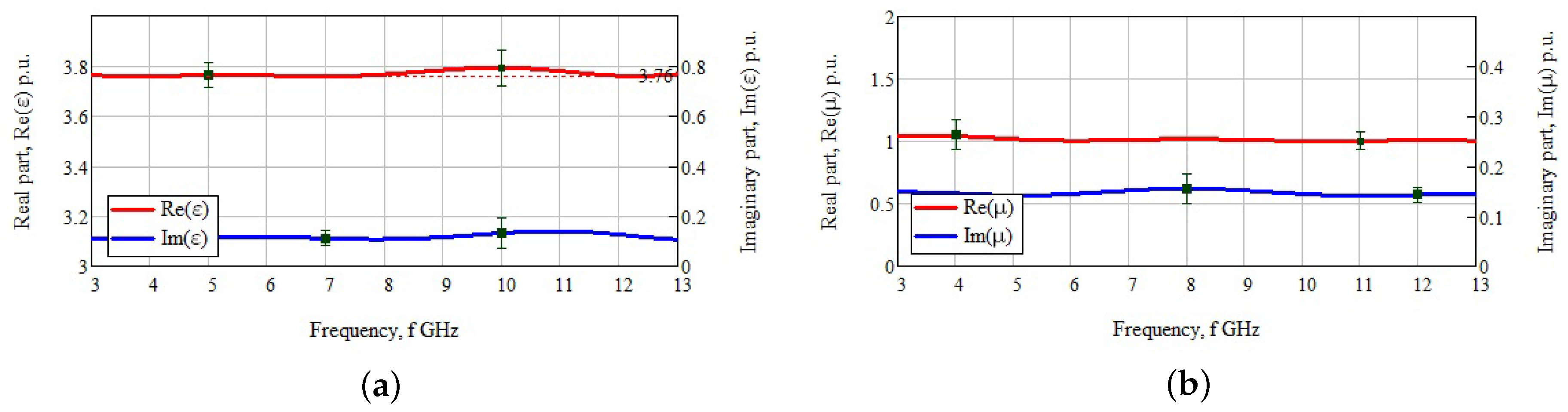
= 2.61. This is 0.3% more than the reference value. The second known material sample was textolite with a thickness of 20.6 mm. Measured values of the relative dielectric permittivity and magnetic permeability are presented below (
Figure 11).
The reference value of the real part of the dielectric permittivity for textolite is
= 3.8 [
26]. The average value of the real part of the dielectric constant according to the graph in
Figure 11 was
= 3.76. The error for the obtained value was 1.1%. The error in the values of the real part of the dielectric constant was no more than 3.2%, which does not exceed the percentage of error for the known methods described in the literature. For the second sample, the measurement data were also averaged. The graph does not show all the results obtained for ease of understanding. Measurement accuracy was based on repeated reading data (100 measurements per sample). To find the error, the discrete sampling formula
was used. After finding a discrete sample, the confidence interval
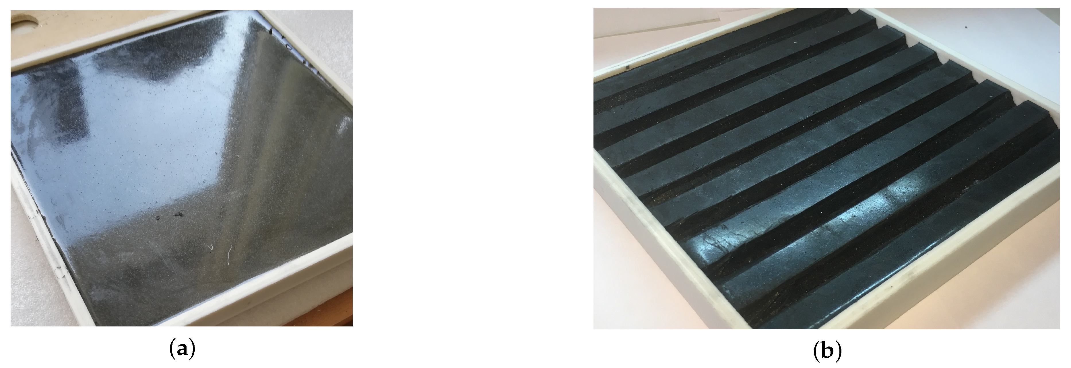
was determined. Confidence intervals are specified for maximum and minimum errors. In addition, two experiments were carried out with a composite material having a high dielectric permittivity. A material composed of polyurethane and graphite was chosen as an example. The percentage of graphite in the used sample was 15%, and polyurethane and hardener were 85% when mixing 1 to 1. The resulting composite was mixed to create a homogeneous mass. In this case, graphite does not dissolve in aqueous solutions and acids, thus forming inclusions of inhomogeneities [
21,
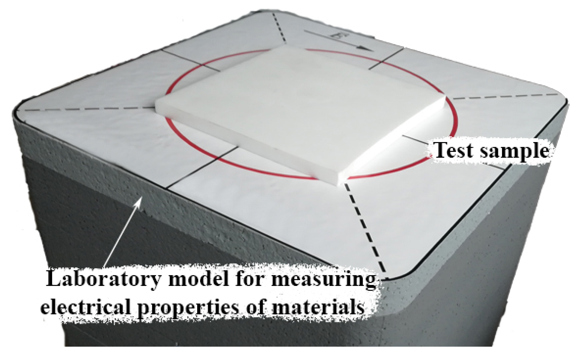
27]. The resulting composite was poured into a plane mold with dimensions 180 × 180 × 15 mm for subsequent measurement using a setup (
Figure 12a). A PNA-L vector network analyzer and dielectric probe kit 85070E slim form from Agilent were used to verify the dielectric values. The actual dimensions of the finished composite were 180 × 180 × 10 mm (
Figure 12b). The measurements were carried out on both installations.
The data obtained using the developed laboratory model were compared with the data obtained by the Agilent installation.
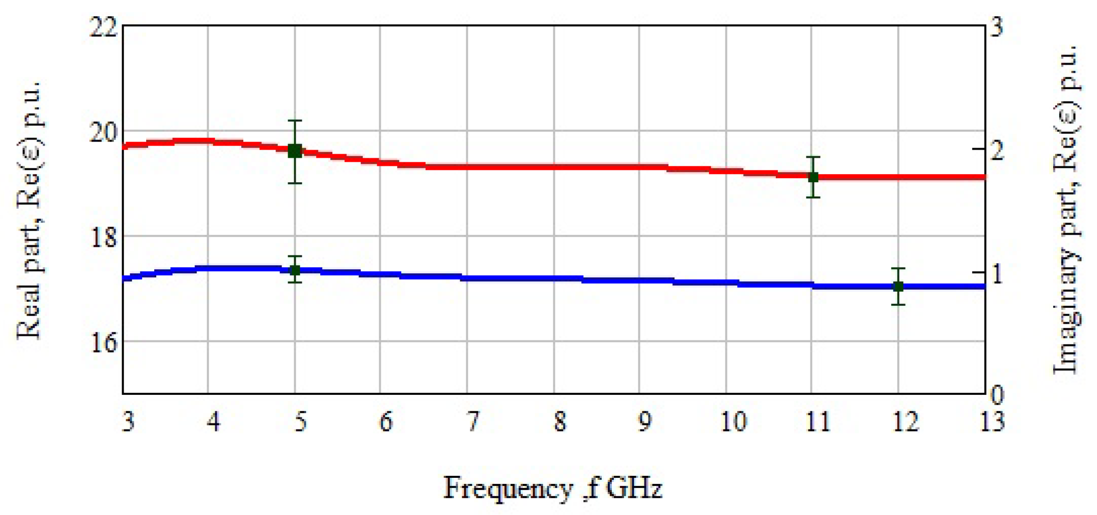
Figure 13 shows the values of the real and imaginary part of the permittivity.
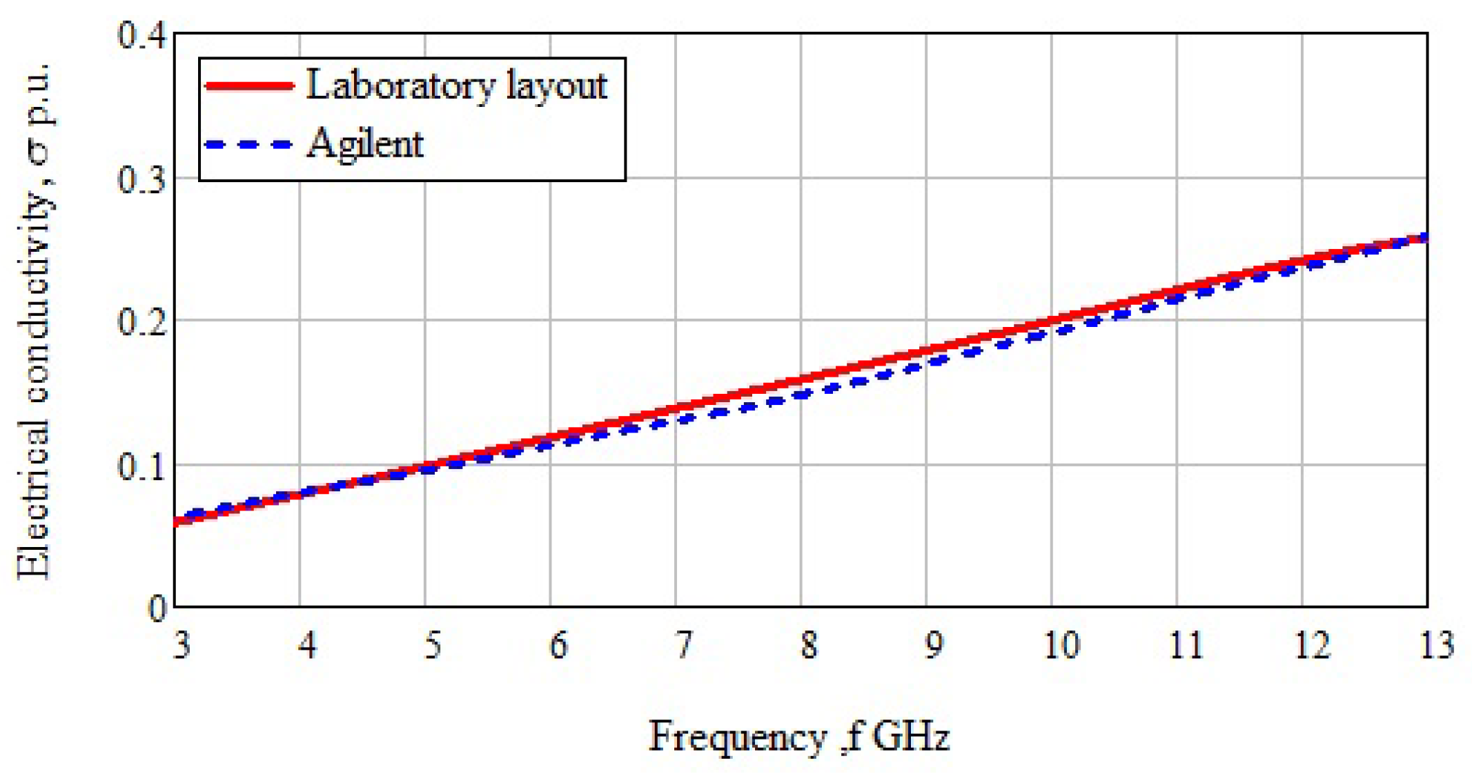
As you can see from the graphs, there is an insignificant difference between the data obtained using Agilent and the data obtained using the created laboratory model. The difference in the obtained data does not exceed 3%, which indicates the high accuracy of the developed laboratory model. The electrical conductivity of the composite material was also calculated. As can be seen from the graph in
Figure 14, the difference between the data obtained using the developed laboratory model and the Agilent setup is also minimal as for the case with the data of the real and imaginary dielectric permittivity.
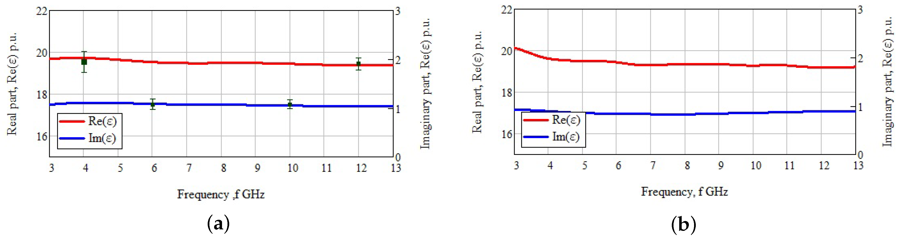
A similar experiment was carried out for the non-plane material. For this, the composite with a high dielectric constant was made an identical size. After that, in the layout, using tools, irregularities were made around the entire perimeter of the material composite (
Figure 12b). Knowing the initial values of the material obtained earlier, comparisons can be made.
Figure 15 shows the values of the real and imaginary parts of the dielectric permittivity versus frequency for creating the non-plane material.
The presented data differ little for both cases. Due to negative phenomena, the error increases up to 3.5%. The maximum deviation at a frequency of 5 GHz. The behavior of the curve is almost identical to the data for a plane sample. The experiments carried out and the data obtained show the possibility of measuring non-plane materials and materials with high roughness.
5. Discussion
The existing methods for measuring the electrophysical parameters of plane samples of materials are quite diverse. However, the carried-out studies have proved that the proposed method is able to accurately and quickly measure the dielectric permittivity and magnetic permeability. In this case, the error in the values of the real part of the dielectric permittivity was no more than 2%. This does not exceed the percentage of error for known methods described in the literature.
In comparison with existing ready-made installations (a line of devices SPEAG Dielectric Assessment Kit (DAK), Keysight Technologies, and others) are based on the existing methods of Nicholson–Ross–Veer, NIST Precision, etc. (these methods are also based on measuring the reflected and transmitted signal) for studying the electrophysical properties of materials, the proposed installation also has advantages. As their analysis showed, these installations are even more demanding in terms of the size, thickness, and surface of materials. They also generally measure only plane and smooth samples. Using a wider bandwidth means more expensive equipment. The use of a vector reflectometer, as in the proposed installation, greatly reduces the cost of the installation and simplifies measurements. In addition, the proposed setup uses a metal parabolic reflectometer, which significantly reduces frequency dispersion. The developed method makes it possible to measure contactless not only smooth, but also rough materials in the region of the beam focusing zone in a smaller frequency range. Experiments carried out on the created laboratory model have shown this possibility.
In the article [
28], using the SPEAG DAK TL-P device, the real part of the dielectric permittivity of plexiglass was measured. The data obtained in the frequency range 5–20 GHz correspond to the data obtained using the installation presented in the article and the developed method.
This method allows you to measure materials with dielectric values in the range from = 1.03 to = 25. The upper threshold is limited by the sensitivity of the Vector reflectometer CABAN R 140 (115 dB), the lower one—to a lesser extent by the quality of the surface of the measured material and to a greater extent by the homogeneity of the focusing beam (along the vertical). This is the last thing that does not allow us to improve the quality. This is about the error. In terms of frequency, the lower threshold is limited by the size of the mirror according to the formula , where a is the antenna aperture, the upper one, by the accuracy of the mirror itself and by “walking” the phase center of the antenna in the feed, that is, by the characteristics of the antenna itself. We now have it up to 13 GHz. Another important factor is the stability of the antenna pattern. Thus, 13 GHz is the limit. To go higher, you need to make a new antenna, for example, from 10 to 40 GHz.
In future, we plan to modernize the installation so as to improve quality. We also plan to introduce additional mathematical data processing to reduce the measurement error. We consider it necessary to expand the range of immersed materials and investigate the applicability of the developed method to such types of modern and popular materials as polymer composite materials.
Such polymeric materials should have biocompatibility, predictable resorption, and the absence of toxicity of both the materials themselves and their degradation products.
6. Conclusions
The method for measuring the electrophysical parameters of materials based on measurements of the transmitted and reflected signals obtained under the condition of ensuring the incidence of a plane wave on the material under study was developed. Numerical and analytical calculations were carried out, and the design of a laboratory model was calculated and developed, with which a number of confirming experiments were carried out. The use of a reflector made it possible not only to achieve a collimated beam on the surface of the measuring laboratory model, but also improve the measurement accuracy. In addition, the proposed design allowed measurements outside the anechoic chamber, was devoid of complex mechanics, and was also not demanding on lateral and/or external radiation, did not require precision expensive equipment, absorbers, and was free from other disadvantages. Mathematical processing excluded extraneous radiation by extracting a useful signal using a time window.
To obtain the most accurate values of electrophysical parameters, the size of the measured sample should not be less than 150 × 150 mm. This is due to the size of the focusing area on the surface of the laboratory model. The thickness of the material must be at least 5 mm. The obtained experimental data showed a high measurement accuracy of simple materials with known values of dielectric permittivity. The level of error for materials such as plexiglass and textolite was 0.3% and 1.1%, respectively.
This research is of great scientific and practical importance.
The scientific significance of this work lies in the fact that there is no focusing lens (we used a parabolic reflector made of metal) made of a dielectric material, which means that there is no frequency dispersion and the data obtained is more accurate when compared to a kit for dielectric measurements, for example, from Keysight Technologies. A single-port measurement was also used, thus there is no need to use a vector analyzer and it is possible to use a vector reflectometer.
In addition, the existing SPEAG installations are contact methods, however in our case the non-contact method and addition of polystyrene is necessary for the convenient placement of the sample. There is no need to prepare material for research. In a large-scale industry, the production of materials requires an examination of the batch. For a line of existing installations, special preparation of the size is required, as well as thickness control, which is not always convenient. Another not unimportant factor of the developed method is the possibility of measuring not ideally smooth samples.


