1. Introduction
Fundamental information processing units of the human brain are interconnected electrically excitable cells—known as neurons and synapses [
1,
2,
3,
4,
5]. Importantly, depending on strength, duration, and repetition rate of the stimuli, the neurons exhibit few unique features, such as leaky integration, automatic fire, and recovery [
5]. On the other hand, a synapse can store the memory typically short- and long-term memories [
1,
6,
7]. Indeed, numerous interconnected neurons and synapses form micro- to nano-scale networks, provide a unique platform to do fault-tolerance, energy-efficient information processing, as well as store memory. This parallel architecture can effectively be implemented to design a robust computing system beyond the conventional von Neumann computer [
3,
5,
8,
9]. Therefore, research efforts have been made in recent years to mimic brain-like functions, artificially for instance, Mott insulator [
5], redox memristors [
1,
5,
10], phase-change memristors [
3,
5,
11], and chalcogenide threshold switches [
12] have been implemented for temporal synaptic integration. Nevertheless, with neuromorphic devices based on these approaches, there still exist a major impediment; specifically, memristors are suffering from nonlinearities, large write noise, and high operative voltage during operation, which in turn pose challenges to apply it for energy efficient brain-like computing [
9,
13]. An alternative could be to design photo-operated devices in contrast to the electric triggering, which in fact work with the real sense simulation, because around 70% of the information that humans get from the outside world comes from vision [
4,
14]. Furthermore, optical triggered devices operate without any contact, and provide promising approaches to realize high operating bandwidth and avoidable heating during operation [
2,
3,
4,
15,
16].
It is worth it to mention here that the visual system is a unique part of the biological neural network, in which retina transforms light signals to electrical pulses, similar to a photodetector [
17,
18,
19].
In fact, spatiotemporal information within the human brain is decoded by spatial and temporal occurrences of spikes within the neurons network. Therefore, to mimic this behavior, it is essential that the device emulates both space and time domains, simultaneously with direct optical inputs, and can conduct processing and memory within a single unit. Previously available visual systems contained separate image sensors, memory, and processing units, which in turn made it more complex and presented serious challenges in terms of large area device integration and power consumption. A simple photodetector that, for instance, could intrinsically show the bio-neuron equivalent desirable dynamics with direct optical pulses, and store the memory simultaneously, would be an effective approach. However, unlike the widely reported artificial synapses, the development of artificial photonic neurons—to the best of our knowledge—has not yet been demonstrated.
Herein, we report a novel approach to design a purely photonic-triggered artificial neuron and synapse with the same architecture and material. The device shows all essential functions of the neuron (such as leaky integration, fire) and short- and long-term memory storage, such as synapse, together in response with direct optical input. This functioning relies on the photo-induced electron-hole pair generation and its trapping via oxygen vacancies in the host material. Further, an array of such devices is capable of pattern classification and supervised learning based on spatiotemporal optical inputs. The present device emulates both the processes and memory functions of the brain, and will be a foundation of the next-generation neuromorphic computing system.
3. Results and Discussion
The biological neuron receives one or more inputs (e.g., A1, A2, etc.) and usually each input is separately weighed to produce an output (C1A1 + C2A2, … CnAn), as depicted schematically in
Figure 1a [
1,
2,
5,
10]. Where, C1, C2, … Cn are the coefficients of weight of each input, containing the values from 0 to 1. We proposed a simple photodetector—termed neuro-photodetector—that could be used to mimic the basic functions of bio-neuron in which light (ultraviolet, UV) pulses work as inputs, and measured photocurrent between two terminals is termed the response form the neuron; see
Figure 1b. In fact, the respective photocurrent (
I1,
I2, …
In) generated by different inputs (e.g.,
P1,
P2, …
Pn) can be summed to produce the resultant output, where
I1,
I2, …
In is the magnitude of the resultant photocurrent (e.g., weighed sum) produced by the
P1,
P2, ….
Pn inputs, respectively. Particularly, the current transport across a photoconductive material can be altered easily by a series of optical pulses, which provide a unique opportunity to mimic the neuron and synapse. In contrast to the conventional photodetectors, a neuro-photodetector must exhibit a time-dependent output current, which in turn allows mimicking the neuron-like behavior. Such a neuro-photodetector is capable to integrate the photocurrent (
Ip) over time, resulting in the
Ip increasing gradually by applying multiple optical inputs, and once the
Ip is above the threshold, the device fires the output like bio-neuron; see
Figure 1c [
9]. The threshold can be defined for specific application in which this artificial neuron is supposed to use. In fact, the output
Ip behavior from the neuro-photodetector with applied pulse intensity/duration could show similar behavior, as is by the bio-neuron. On the other hand, the
Ip decreases gradually during the UV, which is very similar to the leaky behavior of the bio-neuron. The increasing of
Ip with UV illumination, and decreasing after that, are attributed to the UV induced electron-hole pair generation and recombination processes, respectively.
To prepare the neuro-photodetector, we used ZnO materials, in which the transducer is considered the determinant factor of charge transport. Therefore, these defects can be filled out by the photogenerated electron-hole (
e–
h) pairs, resulting in a smooth charge transport or higher photocurrent [
4,
15,
20]. In fact, as illuminating time and/or intensity increases, the defects within the used ZnO layer can be filled out, as shown sequentially from (1) to (4), which in turn increases the
Ip as a fixed measuring voltage, as depicted schematically in
Figure 1d. On the other hand, a slow decay of the
Ip originated from well-known persistent photoconductivity (PPC) due to absorption and desorption of oxygen vacancies [
2,
6,
21].
The schematic of the device is depicted in
Figure 2a, which contains atomic layer deposited ZnO “nanofin” sandwiched between Al and Ag electrodes. More detail of the nanofin-based device fabrication is presented in the Experimental Section and
Figure S1 (Supporting Information). Such kind of arrangements of nanofin provide a unique opportunity to design large-scale and well controlled patterns of devices, which, in fact, could be used for several other neuromorphic applications [
4,
14,
22,
23]. To confirm the effectiveness of our approach of device fabrication, various type of symmetric and asymmetric electrodes, such as Al/ZnO/Al, Ag/ZnO/Ag, Al/ZnO/Ag, and ITO/ZnO/ITO were used; see
Figure S2 (Supporting Information). Indeed, our presented approach provides a unique way to design, well, control geometry (e.g., rectangular, circular, etc.), and size (from µm to cm scale) of the devices over a desired area, see
Figure S2 (Supporting Information).
The growth of the ZnO nanofin was confirmed by planar-view scanning electron microscopy (SEM), as is presented in
Figure 2b. It is interesting to note that ZnO thin film is closely packed, uniform, and conformally sandwiched between vertical Ag and Al, with a thickness of ~80 nm. Following this the sandwiched nature of ZnO is confirmed by energy-dispersive x-ray spectroscopy (EDS), which shows the distribution of aluminum (Al), zinc (Zn), oxygen (O), silver (Ag) elements form the device, see
Figure 2c. It is worth mentioning here that the growth of the ZnO by atomic layer deposition (ALD) has been characterized by various techniques and reported in our recent works.
To understand the charge transport across the nanofin, the typical current-voltage (
I–
V) characteristics of the device in dark and with UV (intensity: 5 mW cm
−2) illumination in the voltage scan range of −1.0 to +1.0 V (ramp rate; 0.01 V s
−1) were performed and depicted in
Figure 2d. The appearance of symmetrical curves under dark and with UV illumination conditions confirms the formation of Ohmic band alignment between the ZnO and Al/Ag. Under dark, the device shows low current (1.12 µA at +1.0 V), which increases to 96.46 µA with UV illumination. The resistance in dark (e.g.,
Roff) was found to be ~1 MΩ, which decreases to
Ron ~ 10.4 kΩ with UV illumination (5 mW cm
−2), confirming significant photocurrent switching on/off ratio (
Ip/
Idark) up to ~10
2, see
Figure 2d. In fact, the
e–
h pairs generated within the ZnO with UV illumination and, thus, the
Ip increases at every measuring voltage.
Further, the transient-photoresponse (
Ip–
t) was measured at +0.6 V after being illuminated with a single UV pulse (4 mW-cm
−2, time, Δ
t = 1 s), see inset of
Figure 2d. During the UV illumination, the
Ip increases rapidly, while it decreases gradually after switching off, indicating the band-to-band excitations and recombination of
e–
h pairs, respectively [
4,
14,
16]. This observation in fact indicates that the device shows significant response to a single UV pulse. In addition, the device shows slow photocurrent decay after UV illumination, the possible reason could be the charge trapping/detrapping by oxygen vacancy. The slow decay of the
Ip in ZnO-based devices has been explained on the basis of the reaction of UV induced holes with chemisorbed surface oxygen, such as h
+ + O
2−(ad) = O
2(g) [
4]. However, UV generated electrons remain within the ZnO, resulting in increases in the overall conductivity at a particularly measuring voltage. Importantly,
Ip decreases after switching off the UV, which is analogue to the leaking nature of the neuron [
9].
To understand and confirm the governing dynamic, we performed the X-ray photoelectron spectroscopy (XPS) measurement of the ZnO after and before the UV illumination; see the presented plots in
Figure S3 (Supporting Information). It was observed that after UV illumination, the XPS peak related to the chemisorbed surface oxygen (e.g., 532.5 eV), reduces significantly, which is due to decreasing in the charge trapping sites related to oxygen vacancies, see
Figure S3 (Supporting Information) [
7]. Slow
Ip decay is a debatable topic; however, as is noted by XPS measurements, the trapping/detrapping of holes via ionized oxygen vacancies provides a show dynamic. Further, to confirm the photoactive nature of the device, the
Ip for a fixed illumination time, (Δ
t = 1 s) was measured by varying pulsed UV intensity from 0.25 to 5 mW cm
−2 and presented in
Figure 2e. Note that the magnitude of
Ip increases linearly with UV intensity most likely due to the increased number of photogenerated carriers [
4,
15,
24]. For statistical analysis, several devices with different areas were prepared and most of them shows similar behavior. The error bar in
Figure 2e is corresponding to the
Ip collected form several devices. The linear dynamic range (LDR), defined as LDR = 20 log(
Ip/
Idark), [
25,
26] is calculated, which is found 40 dB within the illuminating UV intensities (5 mW cm
−2), see
Figure 2e. Moreover, the
Ip for various devices with different areas were measured and depicted in
Figure 2f. Interesting to note that
Ip increases with device area as well, making our approach to design the devices over a desired area.
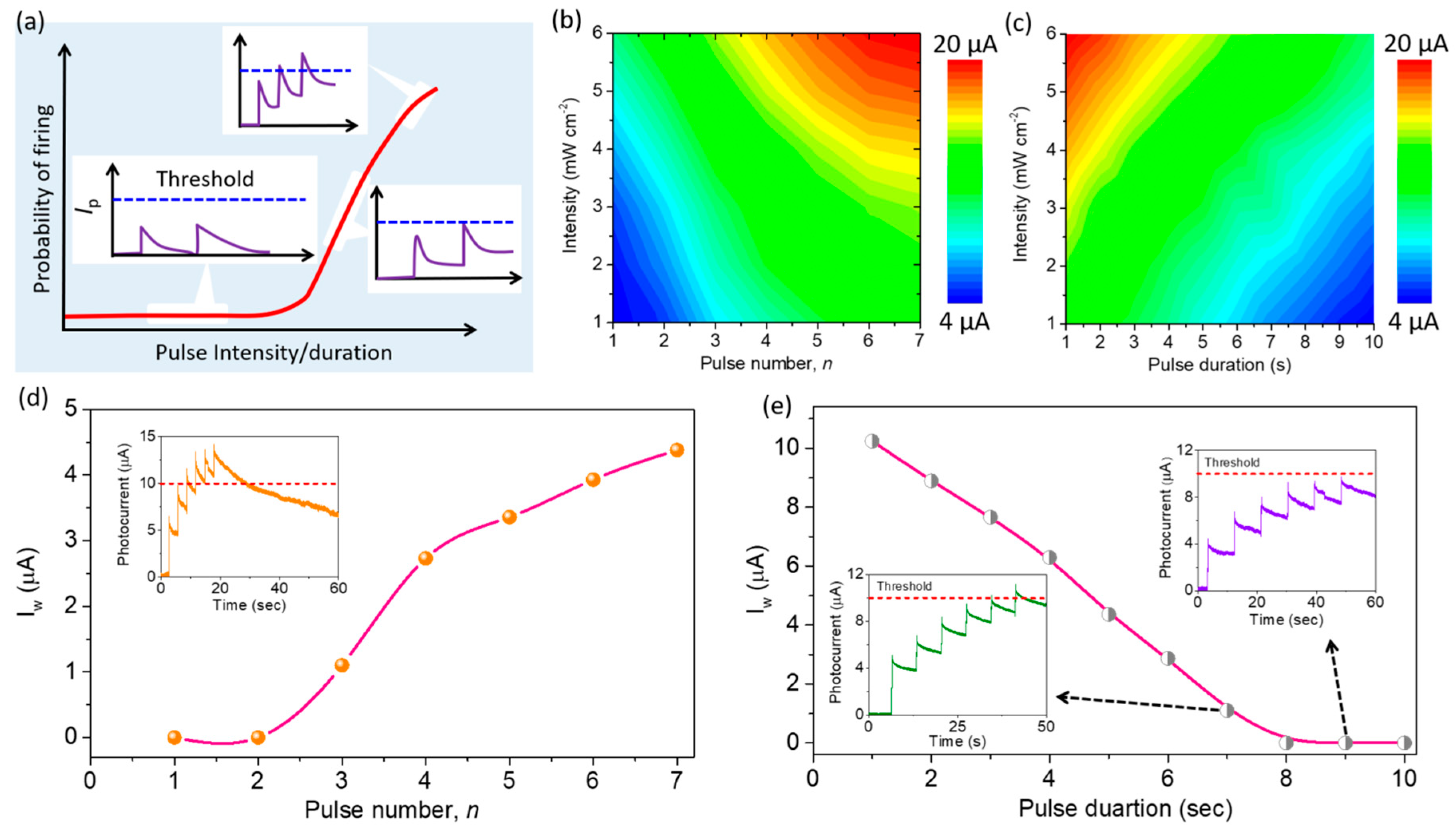
Bio-neuron collects the inputs from connected synapses and integrates them to generate an output signal, if a threshold reached. On the other hand, if integrated, input did not reach to the threshold the signal decays, which is similar to the forgetting the memory. Both these functions, e.g., leaky integration and firing are emulated at device level, using the neuro-photodetector. In fact, decaying of
Ip after UV illumination is corresponding to the ‘leaky’ membrane potential of the bio-neuron, and also a critical dynamical property for forgetting [
5,
10,
27]. This decay time also determines the memory span and is also useful to reset the device after firing the output. To mimic the neutronic behavior, let us assume that spikes (two or more) with similar amplitude however, with different time duration are implemented on the device. In this case, the
Ip corresponding to individual spike is physically summed as per Kirchhoff’s law, and generates the resultant output [
27]. Therefore, longer and intense sequences of input pulses lead to the faster approach to the threshold, resulting in firing, see
Figure 3a. In addition, the
Ip decays gradually towards its initial state, which is like the relaxation process of the human neuron.
Since, the magnitude of
Ip can be modulated by varying the pulse number and/or duration. Therefore, the
Ip generation with of pulse numbers and duration as a function of UV intensity are depicted as 3D plots in
Figure 3b,c, respectively. It is worth to note that higher pulse number (Δ
t = 0.1 s and Δ
d = 1 s) and UV intensity lead to increase the
Ip much faster, see
Figure 3b. The
Ip can also be increases by decreasing the Δ
d of multiple UV pulses, see
Figure 3c, showing the responses of our device to the stimulus train with different pulse intervals ranging from 1 to 10 s. Note that the magnitude of the
Ip depends on the illumination pulse duration and/or number of pulses. The overall change in the
Ip decreases with increasing the time duration between each stimulus. These two figures in fact confirm that, for a selected UV intensity, the
Ip generation can be modulated highly by varying the pulse intervals and/or number, providing an opportunity to choose several parameters to achieve the firing threshold value.
Following the integration capabilities, if threshold for firing condition was set to 10 μA, then the output
Ip above the threshold current (
Iw) as a function of pulse number and pulse duration are plotted in
Figure 3d,e, respectively. Note that for a small number of pulses (
n < 3, Δ
t = 0.2 s, Δ
d = 3 s), the
Iw is close to zero, indicating no firing condition. In contrast, above it, not only the
Iw is non-zero, but also increases with increasing the pulse number, which is because of the integration nature of
Ip. Further,
Figure 3e can systematically summarize the change in the
Iw as a function pulse duration with six modulatory spiking inputs (intensity = 4 mW cm
−2, Δ
t = 0.2 s). These plots again confirmed that the firing properties of the presented neuro-photodetector can be modulated by pulse number and/or pulse duration. These figures present that the threshold nature can be modulated by the applied spikes. For instance, six pulses (intensity = 4 mW cm
−2, Δ
t = 0.2 s, Δ
d = 9 s) cannot generate the current above the threshold, while it can be achieved with short duration, like Δ
d = 6 s. Such a result is one of the great significances for information processing in neuromorphic computing. Overall, the photocurrent integration, very similar to the bio-neuron, can be performed using neuro-photodetector, resulting in providing a unique possibility to mimic temporal information processing.
Another fundamental element, e.g., synapse, connects to two adjacent neurons and its communication strength (synaptic strength/weight) can be modulated by the concentrations of Ca
2+, Na
+, Mg
+, ionic species [
1,
2,
3,
6,
28]. The device based on ZnO shows PPC, which has also been used to emulate the light-induced synaptic functions. In general, origin of learning and memory function of the human brain is believed to depend on the experience-dependent change in the synaptic plasticity, which can be altered by neuronal activities. Therefore, to realize the photo-triggered brain-like memory storage, the
Ip is measured, corresponding to different number of pulses, see
Figure 4a. Unlike conventional memory technologies, depending to the retention time, the human memory is classified into two types viz. short (STM) and long-term memory (LTM) [
4,
6,
7,
29]. Fast current decay is considered as short-term memory (STM), whereas the slow decay is described as long-term memory (LTM). In general, there is no well-defined time frame for STM and LTM. A sequential transformation can be achieved by so-called rehearsal. Since, the device shows functionality of photon sensor, signal processing (via integration) and memory units together; therefore, we utilize an array of the devices for pattern recognition via associative memory. To demonstrate the spatiotemporal processing and learning, an array of 16 devices with ITO electrodes were used. Such an all oxides-based device shows high transmittance in the visible range, particularly making it more useful to design see-through optoelectronic device as well, see the original photograph of the device in
Figure 4b. Proper image processing demands a response to light intensity also to dosage. In fact, the synaptic weights must be sequentially correlated to recognize spatiotemporal pattern. Based on these requirements, this array of neuro-photodetectors work as a photonic sensor together with processing unit, which sense direct optical inputs and adjust synaptic weights, according to the learning rule.
Figure 4c shows the original photo of array of the neuro-photodetector. This array of neuro-photodetectors is simultaneously exposed to optical spike information of different UV intensities; see
Figure 4d,e. The output generated by spatial summated of results of such optical inputs was measured after the 400 s of inputs and displayed in
Figure 4f.
It is interesting to note that the low intensity integration induces a lower sum than the higher intensity. Indeed, above-noticed optical spike combination dependent memory storage behavior could effectively be used to store the information selectively after filtering. The high and low UV intensities are established as the above and below the filter (e.g., threshold). Indeed, the Ip generated above the 4 mW cm−2 is defined as “1” similar to logic output, while below if it does not generate any significant output, such as “0” in logic gates. Therefore, this intensity is referred as a selective intensity. This logical output applies an important role to store the memory similar to the human brain, while the threshold property of the neuro-photodetector is used to store the selective memory.


