Abstract
ZnO is utilized as a promising material for various electronic and energy areas due to its outstanding chemical stability, abundance, non-toxicity, and low cost. However, controlling electronic transport properties of ZnO by facile strategy is still necessary for wider applications. Here, we synthesized reduced graphene oxide incorporated Al-doped ZnO nanocomposite thin film prepared by the electrospray deposition method and investigated the electronic transport behavior. The electron transport in pristine Al-doped ZnO thin film is strongly affected by grain boundary scattering, but significant enhancement of carrier mobility is observed in reduced graphene oxide-incorporated Al-doped ZnO nanocomposite thin film. The results demonstrate that this hybrid strategy with graphene has an important effect on the charge transport behavior in ZnO polycrystalline materials.
1. Introduction
Thin film (TF) materials with high transmittance as well as low electrical resistance have been spotlighted by researchers who may realize next-generation opto-electronic devices, such as displays, solar cells, touch panel, light-emitting diodes, etc [1,2,3,4]. Typically, tin-doped indium oxide (ITO) TF has been used as a transparent electrode; however, its use will be limited due to the scarcity, toxicity, and low stability of indium [5,6,7]. ZnO is a direct transition-type semiconductor material with a band gap energy of 3.3 eV, and it has a large exciton binding energy of 60 meV even at room temperature. These qualities suggest that it could be considered as a potential alternative material for ITO due to its transparency, non-toxicity and cost-efficiency [8,9].
However, ZnO TF has a relatively high electrical resistance that restrains the wider use of ZnO. In order to reduce the electrical resistance of ZnO, many researchers have been using cation doping against the Zn site. Tseng et al. modified the physicochemical properties of ZnO to improve the performance via Al doping [10], and Liang et al. prepared Ga-doped ZnO to increase electrical conductivity [11]. It was revealed that ZnO TF doped with group-III elements (B, Al, Ga, In) exhibited low resistivity and high transparency in the visible region. Because of the similar covalent bonding lengths of Zn-O and Al-O, Zn2+ ions in the ZnO matrix can be structurally stable even when substituted with Al3+, and electrical conductivity can be improved by increasing charge carriers [12,13,14]. Nevertheless, the electronic transport behavior of Al-doped ZnO (AZO) TF is largely influenced by grain boundary scattering in electronic transmission because it consists of crystallization of several nanoscale sizes.
Recently, hybrid nanostructure technologies with carbon-based composites have been applied to overcome the mechanical, chemical, electrical, and opto-electronic properties [15,16,17,18,19,20]. Among the diverse carbon nanomaterials, reduced graphene oxide (RGO) has been considered as one of the most attractive material for next-generation electronics since it has high charge carrier mobility originating from a two-dimensional (2D) atomic structure of carbon with sp2 hybridization [21,22,23]. In this study, we focus on the effect of graphene on the charge transport behavior in the AZO-RGO nanocomposite (NC) TF. The AZO-RGO nanocomposite thin film (NCTF) was deposited on a SiO2/Si substrate using the electrospray deposition process with RGO-dispersed precursor solution. Compared to the pristine AZO TF, the AZO-RGO NCTF shows enhanced mobility resulting from an increase in carrier concentration. Grain boundary scattering could be suppressed due to the Schottky barrier reduction with RGO incorporation between the grain boundary, resulting in an increased charge transport behavior in the AZO-RGO NCTF. Therefore, we provide a facile strategy to fabricate advanced transparent conducting film by incorporating RGO on AZO TF, and this nanocomposite TF could be a practical form of technology for controlling electronic transport behavior for various opto-electronic applications.
2. Materials and Methods
2.1. Sample Preparation
The AZO-RGO NCTF was prepared using electrospray deposition on a SiO2 (300 nm)/Si substrate. The substrate surface was cleaned by sonicating in acetone, ethanol and de-ionized water, and modified by plasma treatment at 200 W for 5 min under an oxygen atmosphere to increase the hydrophilicity. The precursor solution for the deposition of AZO-RGO NCTF was prepared by mixing zinc acetate dihydrate (Zn(CH3COO)2∙2H2O), aluminum chloride hexahydrate (AlCl3∙6H2O) as a dopant material, and graphene oxide (GO, 5 wt%) in ethylene glycol (C2H4(OH)2) solvent. The precursor solution was sprayed through the nozzle (inner diameter: 0.1 mm, outer diameter: 0.23 mm) onto the heated substrate. The applied voltage, precursor solution feed rate, deposition time and hot plate temperature were maintained at 10 kV, 2 μL min−1, 30 min and 150 °C, respectively. As-deposited film was subjected to rapid thermal annealing (RTA) at 600 °C for 30 min under an inert atmosphere. This process allowed the formation of single-phase ZnO and a reduction of graphene oxide (GO). Furthermore, AZO TF was also fabricated using the precursor solution without GO under the same deposition conditions in order to investigate the effect of graphene on the charge transport behavior.
2.2. Characterization Methods
The microstructures of the samples were characterized using an X-ray diffractometer (XRD, DMAX-3C, Rigaku Corporation, Tokyo, Japan) with Cu Kα radiation, a scanning electron microscope (SEM, Verios 460L, FEI Company, Hillsboro, OR, USA), and a transmission electron microscope (TEM, JEM-4010, JEOL, Ltd., Akishima, Japan) operating at an acceleration voltage of 400 kV. Furthermore, X-ray photoelectron spectroscopy (XPS, PHI 5000 VersaProbe, ULVAC-PHI, Inc., Chigasaki, Japan) was utilized to investigate C1s core level of RGO in the NCTF. The room temperature charge transport properties in the samples were characterized by using a Hall measurement system (ResiTest 8300, Toyo Corporation, Tokyo, Japan) under a magnetic field of 0.57 T.
3. Results and Discussion
Figure 1 shows the electrospray deposition process for synthesizing AZO TF and AZO-RGO NCTF. The precursor solution with or without GO is sprayed on the heated substrate, and the TF could be simply obtained on the SiO2/Si substrate. The TF samples are followed by the RTA process for crystallization of AZO as well as the reduction of GO. Figure 2a represents the XRD patterns of the AZO TF and AZO-RGO NCTF. The strong peaks at 56.13° could be indexed to Si(311) from the substrate. The main peaks of both samples are obtained from the wurtzite structure of ZnO (JCPDS card no. 36-1451), indicating that single phase ZnO was successfully prepared. Furthermore, no secondary phase is observed in the XRD pattern of the AZO-RGO NCTF, and the peak positions in the NCTF are not changed with the RGO incorporation due to the low RGO content.
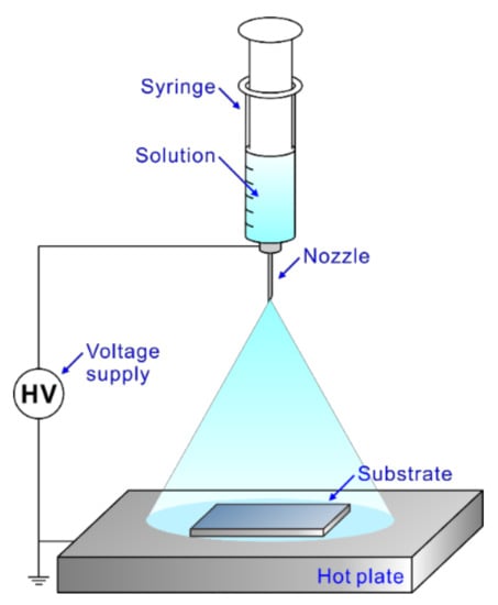
Figure 1.
Schematic diagram of electrospray deposition used in this study.
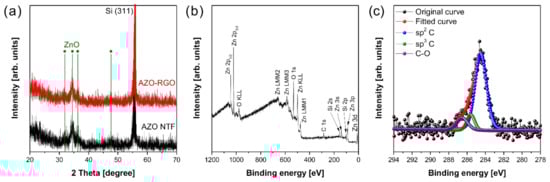
Figure 2.
(a) XRD spectra of Al-doped ZnO thin film (AZO TF) and AZO-reduced graphene oxide (RGO) NCTF. (b) XPS wide scan and (c) C1s core level spectra of AZO-RGO nanocomposite thin film (NCTF).
The XPS was carried out to investigate the chemical composition in the NCTF. The survey scan of XPS spectrum reveals that the NCTF has only Zn, O, C, and Si elements (Figure 2b). The Si peaks were originated from the substrate, and no Al signals were detected due to its low doping concentration. The C1s core level spectrum shows the chemical binding state of carbon atoms in RGO, and it was deconvoluted into sp2 C centered at 284.5 eV, sp3 C centered at 285.6 eV, and C-O centered at 286.6 eV [24,25]. The ratio of sp2 C/sp3 C is sensitive to the degree of oxidation in RGO, and it decreases with the increasing oxidation level of RGO. It was reported that the ratio measured from the XPS spectrum of highly reduced graphene oxide (HRGO) was 2.15 [26]. In our case, the ratio of sp2 C/sp3 C in the AZO-RGO NCTF was estimated to be 10.8, indicating that GO was effectively reduced during the RTA process.
Figure 3 shows the SEM micrographs of the cross-section and plane view of samples. The cross-section SEM micrographs (Figure 3a,c) show the thickness of the samples was 200 nm. Furthermore, the plane-view SEM micrographs of the AZO TF and AZO-RGO NCTF (shown in Figure 3b,d) show that a dense TF was deposited on the SiO2/Si substrate. To obtain a detailed microstructure of the AZO TF and AZO-RGO NCTF, TEM analysis are conducted (Figure 4). Figure 4a,c show bright-field TEM analysis of the AZO TF and AZO-RGO NCTF, and the samples were comprised of primary nanograins (<10 nm), which indicates that the existence of RGO does not affect the grain size of the AZO-RGO NCTF. The selected area electron diffraction patterns obtained from Figure 4a,c (insets) revealed a set of distinct rings corresponding to hexagonal ZnO. Furthermore, Figure 4b shows a high-resolution TEM micrograph of the AZO TF, which shows an interplanar spacing of 0.28 nm corresponding to the lattice spacing of the ZnO plane. Figure 4d shows the high-resolution TEM image of AZO-RGO NCTF, and the red arrows indicate that RGO dispersed in the AZO-RGO NCTF, which shows the uniform dispersion of RGO without aggregation. The inset in Figure 4d shows the interlayer spacing of RGO (0.345 nm) obtained from the red rectangular box, which is slightly increased with that of graphite (0.335 nm) [27]. Beside the ratio of sp2 C/sp3 C in XPS spectrum, the interlayer spacing of RGO is also strongly dependent on its degree of oxidation [28,29,30]. It was reported that the interlayer spacing of HRGO, with a relative carbon to oxygen ration of 10, was 0.364 nm [29]. This means that the GO could be effectively reduced via the RTA process, which is consistent with the XPS result shown in Figure 2b.
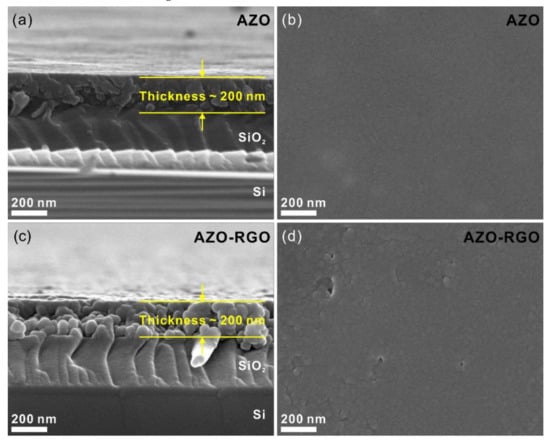
Figure 3.
(a) Cross-sectional and (b) plane view SEM micrographs of AZO TF, (c) Cross-sectional and (d) plane view SEM micrographs of AZO-RGO NCTF.
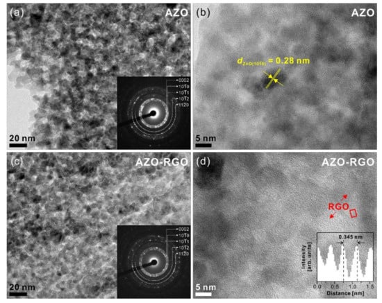
Figure 4.
(a) Bright-field and (b) high-resolution TEM micrographs of AZO TF. (c) Bright-field and (d) high-resolution TEM micrographs of AZO-RGO NCTF. Insets in (a) and (c) represent the selected area electron diffraction patterns. Inset in (d) shows the intensity profile obtained from the red rectangular box.
Figure 5 represents the charge transport properties of the AZO TF and AZO-RGO NCTF at room temperature compared to those of ZnO single crystals [31,32,33,34] and epitaxial thin films [35,36,37,38] in the literature. The empirical curve developed by Masetti et al., which describes the dependence of the single crystalline ZnO mobility versus carrier concentration, is also depicted as a green solid line in Figure 5a [39,40]. The mobility of the AZO TF without RGO was 10.3 cm2 V−1 s−1, which is far below that of single crystalline ZnO. This result indicates that the charge transport properties in the AZO TF were limited by numerous nanograins, as shown in Figure 4a. Generally, the charge transport in polycrystalline ZnO is strongly influenced by the Schottky barrier at the grain boundaries, which is an electrostatic potential barrier originating from the trapped electrons. This Schottky barrier induces severe charge scattering in polycrystalline ZnO [41]. The RGO could release the trapped electrons in the grain boundary regions in AZO-RGO NCs, leading to the single crystal-like charge transport caused by the relieved Schottky barrier [23]. A considerable improvement of mobility (29.1 cm2 V−1 s−1) with increased carrier concentration was obtained in the AZO-RGO NCTF, leading to the reduction of resistivity (shown in Figure 5b). Since the grain size of the AZO TF and AZO-RGO NCTF (<10 nm) is very small, the charge transport behavior in our system could be strongly affected by grain boundary. Although the mobility of the AZO-RGO NCTF was still lower than that of the single crystalline ZnO due to the small size of nanograins (<10 nm), we confirmed that the incorporation of RGO in AZO TF is an effective strategy for enhancing the charge transport properties in AZO.
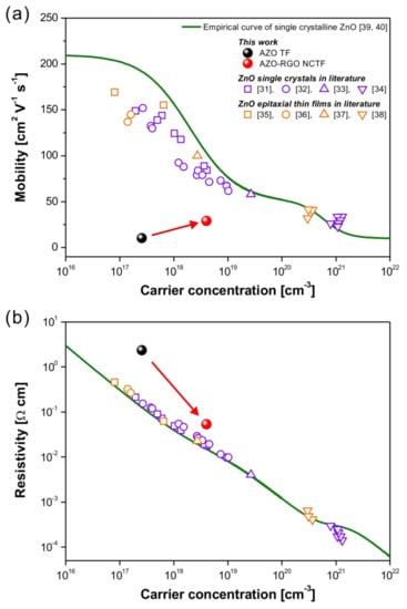
Figure 5.
Carrier-concentration-dependent (a) mobility and (b) resistivity in AZO TF and AZO-RGO NCTF at room temperature. For comparison, mobility and resistivity values of ZnO single crystals [31,32,33,34] and epitaxial thin films [35,36,37,38] in the literature are also shown.
4. Conclusions
We proposed a hybrid strategy for synthesizing AZO incorporated with RGO for controlling charge transport properties of oxide materials. We focused on the effect of RGO on the charge transport behavior of AZO TF. Microstructural characterization revealed that the samples comprised nanosized grains (<10 nm), and RGO was well dispersed in the AZO-RGO NCTF without aggregation. The electron transport in AZO TF was strongly affected by grain boundary scattering, but enhanced charge transport behavior was observed in the AZO-RGO NCTF. Given that grain boundary scattering can be suppressed through the incorporated RGO, the mobility of the AZO-RGO NCTF is improved with increased carrier concentration. Our results demonstrate that our hybrid strategy with RGO could have a positive effect on the charge transport behavior in oxide materials.
Author Contributions
Conceptualization, W.H.N.; methodology, J.-H.L., H.M.J.; formal analysis, J.-M.O., W.H.N., W.H.S.; investigation, H.S., J.-H.L., H.M.J.; data curation, J.-M.O., W.H.N., W.H.S.; writing—original draft preparation, W.H.N.; writing—review and editing, W.H.S., J.Y.C.; visualization, H.M.J., W.H.N.; supervision, W.H.S., W.-S.S., J.Y.C.; project administration, W.H.N.; funding acquisition, W.H.S., W.H.N., H.M.J., W.-S.S. All authors have read and agreed to the published version of the manuscript.
Funding
This work was supported by the Korea Institute of Ceramic Engineering and Technology (KPP19001), and by the Technology Innovation Program (10083640) through the Korea Evaluation Institute of Industrial Technology funded by the Ministry of Trade, Industry and Energy, Republic of Korea, and by the Basic Science Research Program through the National Research Foundation of Korea (NRF) funded by the Ministry of Education, Science and Technology (2019R1A6A1A11055660, 2019R1F1A1059591, 2020R1F1A1071311).
Conflicts of Interest
The authors declare no conflict of interest.
References
- Wassei, J.K.; Kaner, R.B. Graphene, a promising transparent conductor. Mater. Today 2010, 13, 52–59. [Google Scholar] [CrossRef]
- Liu, C.-H.; Chang, Y.-C.; Norris, T.B.; Zhong, Z. Graphene photodetectors with ultra-broadband and high responsivity at room temperature. Nat. Nanotechnol. 2014, 9, 273–278. [Google Scholar] [CrossRef] [PubMed]
- Nag, A.; Mitra, A.; Mukhopadhyay, S.C. Graphene and its sensor-based applications: A review. Sensor. Actuat. A Phys. 2018, 270, 177–194. [Google Scholar] [CrossRef]
- Reddy, D.; Register, L.F.; Carpenter, G.D.; Banerjee, S.K. Graphene field-effect transistors. J. Phys. D Appl. Phys. 2011, 45, 019501. [Google Scholar] [CrossRef]
- Minami, T. Substitution of transparent conducting oxide thin films for indium tin oxide transparent electrode applications. Thin Solid Film. 2008, 516, 1314–1321. [Google Scholar] [CrossRef]
- Minami, T.; Miyata, T. Present status and future prospects for development of non-or reduced-indium transparent conducting oxide thin films. Thin Solid Films 2008, 517, 1474–1477. [Google Scholar] [CrossRef]
- Yin, J.; Zhou, H.; Liu, Z.; Nie, Z.; Li, Y.; Qi, X.; Chen, B.; Zhang, Y.; Zhang, X. Indium-and platinum-free counter electrode for green mesoscopic photovoltaics through graphene electrode and graphene composite catalysts: Interfacial compatibility. ACS Appl. Mater. Interfaces 2016, 8, 5314–5319. [Google Scholar] [CrossRef] [PubMed]
- Shan, F.; Yu, Y. Band gap energy of pure and Al-doped ZnO thin films. J. Eur. Ceram. Soc. 2004, 24, 1869–1872. [Google Scholar] [CrossRef]
- Lee, J.-S.; Park, K.; Kang, M.-I.; Park, I.-W.; Kim, S.-W.; Cho, W.K.; Han, H.S.; Kim, S. ZnO nanomaterials synthesized from thermal evaporation of ball-milled ZnO powders. J. Cryst. Growth 2003, 254, 423–431. [Google Scholar] [CrossRef]
- Tseng, Z.-L.; Chiang, C.-H.; Chang, S.-H.; Wu, C.-G. Surface engineering of ZnO electron transporting layer via Al doping for high efficiency planar perovskite solar cells. Nano Energy 2016, 28, 311–318. [Google Scholar] [CrossRef]
- Liang, X. Thermoelectric transport properties of naturally nanostructured Ga–ZnO ceramics: Effect of point defect and interfaces. J. Eur. Ceram. Soc. 2016, 36, 1643–1650. [Google Scholar] [CrossRef]
- Akdağ, A.; Budak, H.; Yılmaz, M.; Efe, A.; Büyükaydın, M.; Can, M.; Turgut, G.; Sönmez, E. Structural and morphological properties of Al doped ZnO nanoparticles. J. Phys. Conf. Ser. 2016, 707, 012020. [Google Scholar]
- Sarma, B.; Barman, D.; Sarma, B.K. AZO (Al: ZnO) thin films with high figure of merit as stable indium free transparent conducting oxide. Appl. Surf. Sci. 2019, 479, 786–795. [Google Scholar] [CrossRef]
- Nam, W.H.; Lim, Y.S.; Choi, S.-M.; Seo, W.-S.; Lee, J.Y. High-temperature charge transport and thermoelectric properties of a degeneratly Al-doped ZnO nanocomposite. J. Mater. Chem. 2012, 22, 14633–14638. [Google Scholar] [CrossRef]
- Lekawa-Raus, A.; Patmore, J.; Kurzepa, L.; Bulmer, J.; Koziol, K. Electrical properties of carbon nanotube based fibers and their future use in electrical wiring. Adv. Funct. Mater. 2014, 24, 3661–3682. [Google Scholar] [CrossRef]
- Avouris, P.; Freitag, M.; Perebeinos, V. Carbon-nanotube photonics and optoelectronics. Nat. Photonics 2008, 2, 341–350. [Google Scholar] [CrossRef]
- Schroeder, V.; Savagatrup, S.; He, M.; Lin, S.; Swager, T.M. Carbon nanotube chemical sensors. Chem. Rev. 2019, 119, 559–663. [Google Scholar] [CrossRef]
- Papageorgiou, D.G.; Kinloch, I.A.; Young, R.J. Mechanical properties of graphene and graphene-based nanocomposites. Prog. Mater. Sci. 2017, 90, 75–127. [Google Scholar] [CrossRef]
- Probst, N.; Grivei, E. Structure and electrical properties of carbon black. Carbon 2002, 40, 201–205. [Google Scholar] [CrossRef]
- Li, T.F.; Kaneko, T.; Hatakeyama, R. Electrical transport properties of fullerene peapods interacting with light. Nanotechnology 2008, 19, 41. [Google Scholar] [CrossRef]
- Huang, X.; Zeng, Z.; Fan, Z.; Liu, J.; Zhang, H. Graphene-based electrodes. Adv. Mater. 2012, 24, 5979–6004. [Google Scholar] [CrossRef] [PubMed]
- Geim, A.K.; Novoselov, K.S. The rise of graphene. Nat. Mater. 2007, 6, 183–191. [Google Scholar] [CrossRef] [PubMed]
- Nam, W.H.; Kim, B.B.; Seo, S.G.; Lim, Y.S.; Kim, J.-Y.; Seo, W.-S.; Choi, W.K.; Park, H.-H.; Lee, J.Y. Structurally nanocrystalline-electrically single crystalline ZnO-reduced graphene oxide composites. Nano Lett. 2014, 14, 5104–5109. [Google Scholar] [CrossRef] [PubMed]
- Fan, Z.-J.; Kai, W.; Yan, J.; Wei, T.; Zhi, L.-J.; Feng, J.; Ren, Y.-M.; Song, L.-P.; Wei, F. Facile synthesis of graphene nanosheets via Fe reduction of exfoliated graphite oxide. ACS Nano 2011, 5, 191–198. [Google Scholar] [CrossRef] [PubMed]
- Mattevi, C.; Eda, G.; Agnoli, S.; Miller, S.; Mkhoyan, K.A.; Celik, O.; Mastrogiovanni, D.; Granozzi, G.; Garfunkel, E.; Chhowalla, M. Evolution of electrical, chemical, and structural properties of transparent and conducting chemically derived graphene thin film. Adv. Funct. Mater. 2009, 19, 2577–2583. [Google Scholar] [CrossRef]
- Krishnamoorthy, K.; Veerapandian, M.; Yun, K.; Kim, S.-J. The chemical and structural analysis of graphene oxide with different degrees of oxidation. Carbon 2013, 53, 38–49. [Google Scholar] [CrossRef]
- Ni, Z.H.; Wang, H.M.; Kasim, J.; Fan, H.M.; Yu, T.; Wu, Y.H.; Feng, Y.P.; Shen, Z.X. Graphene thickness determination using reflection and contrast spectroscopy. Nano Lett. 2007, 7, 2758–2763. [Google Scholar] [CrossRef]
- Park, S.; An, J.; Potts, J.R.; Velamakanni, A.; Murali, S.; Ruoff, R.S. Hydrazine-reduction of graphite- and graphene oxide. Carbon 2011, 49, 3019–3023. [Google Scholar] [CrossRef]
- Shin, K.-H.; Jang, Y.; Kim, B.-S.; Jang, J.; Kim, S.H. Highly conductive reduced graphene oxide produced via pressure-assisted reduction at mild temperature for flexible and transparent electrodes. Chem. Commun. 2013, 49, 4887–4889. [Google Scholar] [CrossRef]
- Rajaura, R.S.; Srivastava, S.; Sharma, V.; Sharma, P.K.; Lal, C.; Singh, M.; Palsania, H.S.; Vijay, Y.K. Role of interlayer spacing and functional group on the hydrogen storage properties of graphene oxide and reduced graphene oxide. Int. J. Hydrog. Energy 2016, 41, 9454–9461. [Google Scholar] [CrossRef]
- Rupprecht, H. Über konzentration und beweglichkeit von elektronen in zinkoxydeinkristallen mit definierten zusätzen. J. Phys. Chem. Soilds 1958, 6, 144–154. [Google Scholar] [CrossRef]
- Kobayashi, J.; Ohashi, N.; Sekiwa, H.; Sakaguchi, I.; Miyamoto, M.; Wada, Y.; Adachi, Y.; Matsumoto, K.; Haneda, H. Properties of gallium- and aluminum-doped bulk ZnO obtained from single-crystals grown by liquid phase epitaxy. J. Cryst. Growth 2009, 311, 4408–4413. [Google Scholar] [CrossRef]
- Loukya, B.; Sowjanya, P.; Dileep, K.; Shipra, R.; Kanuri, S.; Panchakarla, L.S.; Datta, R. Controlling structural quality of ZnO thin film on c-plane sapphire during pulsed laser deposition. J. Cryst. Growth 2011, 329, 20–26. [Google Scholar] [CrossRef]
- Igasaki, Y.; Saito, H. The effects of deposition rate on the structural and electrical properties of ZnO:Al films deposited on (1120) oriented sapphire substrates. J. Appl. Phys. 1991, 70, 3613–3619. [Google Scholar] [CrossRef]
- Chu, S.; Morshed, M.; Li, L.; Huang, J.; Liu, J. Smooth surface, low electron concentration, and high mobility ZnO films on c-plane sapphire. J. Cryst. Growth 2011, 325, 36–40. [Google Scholar] [CrossRef]
- Miyamoto, K.; Sano, M.; Kato, H.; Yao, T. High-electron-mobility ZnO epilayers grown by plasma-assisted molecular beam epitaxy. J. Cryst. Growth 2004, 265, 34–40. [Google Scholar] [CrossRef]
- Ohtomo, A.; Kimura, H.; Saito, K.; Makino, T.; Segawa, Y.; Koinuma, H.; Kawasaki, M. Lateral grain size and electron mobility in ZnO epitaxial films grown on sapphire substrates. J. Cryst. Growth 2000, 214/215, 284–288. [Google Scholar] [CrossRef]
- Ellmer, K.; Vollweiler, G. Electrical transport parameters of heavily-doped zinc oxide and zinc magnesium oxide single and multilayer films heteroepitaxially grown on oxide single crystals. Thin Solid Film. 2006, 496, 104–111. [Google Scholar] [CrossRef]
- Masetti, G.; Severi, M. Modeling of carrier mobility against carrier concentration in arsenic-, phosphorus-, and boron-doped silicon. IEEE Trans. Electron Devices 1983, 30, 764–769. [Google Scholar] [CrossRef]
- Ellmer, K. Resistivity of polycrystalline zinc oxide films: Current status and physical limit. J. Phys. D Appl. Phys. 2001, 34, 3097–3108. [Google Scholar] [CrossRef]
- Gupta, T.K.; Carlson, W.G. A grain-boundary defect model for instability/stability of a ZnO varistor. J. Mater. Sci. 1985, 20, 3487–3500. [Google Scholar] [CrossRef]


Publisher’s Note: MDPI stays neutral with regard to jurisdictional claims in published maps and institutional affiliations. |
© 2020 by the authors. Licensee MDPI, Basel, Switzerland. This article is an open access article distributed under the terms and conditions of the Creative Commons Attribution (CC BY) license (http://creativecommons.org/licenses/by/4.0/).