Review

Micro-LED as a Promising Candidate for High-Speed Visible Light Communication

1
Department of Photonics and Graduate Institute of Electro-Optical Engineering, College of Electrical and Computer Engineering, National Chiao Tung University, Hsinchu 30010, Taiwan
2
Department of Electrical Engineering and Computer Engineering, National Chiao Tung University, Hsinchu 30010, Taiwan
3
Department of Electronic Science, Fujian Engineering Research Center for Solid-State Lighting, Xiamen University, Xiamen 361005, China
4
Institute of Photonic System, National Chiao Tung University, Tainan 71150, Taiwan
5
Graduate Institute of Photonics and Optoelectronics and Department of Electrical Engineering, National Taiwan University, No. 1, Sec. 4, Roosevelt Road, Taipei 10617, Taiwan
*
Authors to whom correspondence should be addressed.
The authors contributed equally to this work.
Appl. Sci. 2020, 10(20), 7384; https://doi.org/10.3390/app10207384
Submission received: 10 September 2020 / Revised: 3 October 2020 / Accepted: 8 October 2020 / Published: 21 October 2020
(This article belongs to the Section Optics and Lasers)

Abstract

:
Visible Light Communication (VLC) technology is an emerging technology using visible light modulation that, in the modern world, will mainly facilitate high-speed internet connectivity. VLC provides tremendous advantages compared to conventional radio frequency, such as a higher transmission rate, high bandwidth, low-power consumption, no health hazards, less interference, etc., which make it more prominent in recent days. Due to their outstanding features, including low cost, low power consumption, etc., µ-light-emitting diodes (LEDs) have gained considerable attention for VLC implementation, but mostly for the ability to be used for lighting as well as communications. In this review paper, we will focus mainly on recent developments in VLC applications and various factors affecting the modulation bandwidth of VLC devices. Numerous factors, such as quantum confined stark effect (QCSE), carrier lifetime, carrier recombination time, crystal orientation, etc. affect the modulation bandwidth of LEDs, and more information will be discussed in the following sections. This paper will focus on VLC applications based on LEDs but mainly on semipolar μ-LEDs and μ-LED-based arrays with high bandwidths. Another important application of VLC is underwater optical wireless communication (UOWC), which has drawn a huge interest in marine exploration and underwater connectivity, but still faces some challenges because visible light is being used. In addition, this paper will focus on how the current VLC system modulation bandwidth can be enhanced. Many methods have been introduced, such as decreasing the active layer thickness or effective active area or using doping, but the bandwidth is restricted by the recombination time when the system configuration reaches its limit. Therefore, it is important to find alternative ways such as optimizing the system, using the blue filter or using the equalization technology, which will be addressed later. Overall, this review paper provides a brief overview of the VLC-based system performance and some of its potential prospects.

1. Introduction

Wireless communications have driven the desire for improved connectivity since its inception, and it has been used since the time when humans used smoke signals and birds for wireless communication. Robert Hooke subsequently discovered mobile panels in 1684 that coded the letters of the alphabet. The optical telegraph was developed towards the end of the 18th century and can relay coded words over long distances. Since then, many developments have advanced with telecommunication technologies in response to customer demands for faster and more reliable connectivity. When it comes to radio communication, using coded information transmitted through electromagnetic (EM) waves, after the advent of electromagnetic waves, wireless telegraphy and the invention of radio, wireless communication has gone through many paradigm changes [1,2]. EM waves have a wide variety of applications in today’s life that include numerous uses of mobile phone communication, radio broadcasting, Wi-Fi, medical applications, etc., and EM waves can be categorized into radio, infrared, visible, ultraviolet, etc. Among those, radio frequency (RF) is the one that is the widely used portion of the EM spectrum for communication purposes, as RF transmission occurs at light speed, does not require a travel medium and can travel long distances. In addition, RF does not require a line of sight between the transmitter and receiver, is not susceptible to interference from bright to light sources, and has low interference in the frequency band and broad area coverage [1]. RF communication, however, faces some challenges such as interference, as the use of cell phones in aircraft causes interference with communication and navigation systems; bandwidth limitations, security issues, as they can easily penetrate through walls; transmission power limitations, as they can result in risks to human safety; power inefficiency; etc. [3,4,5,6]. Therefore, developing an alternative solution is imperative in order to solve these challenges.
Visible Light Communication (VLC) is evolving as a workaround for wireless communications networks to tackle crowded radio spectrum. VLC is an emerging technology that employs visible light for communication to facilitate high-speed internet connectivity exclusively in the indoor environment. In VLC, data are transmitted by modulating the amplitude of an optical source that operates at much faster speed within the visible range of the EM spectrum, and, thus, due to its high switching rate, light-emitting diodes (LEDs) are the most desirable light source for VLC. The VLC systems occupy the EM spectrum ranging from 380 nm to 750 nm corresponding to the frequency range of 430 THz to 790 THz, and the availability of this wide bandwidth in VLC solved the problem of low bandwidth in RF communication. Security issues in RF communication can be solved in VLC, as optical source lights cannot pass through opaque bodies and confined in an intended region, nor does VLC cause any interference with the RF signals resulting in enhancing VLC security [7]. It is a well-known fact that exposure to high-intensity RF signals can result in burns and damage to body tissues, thus limiting the system’s own transmitting power, which affects system performance [8]. VLC uses LEDs as the non-harmful optical source for the human body, which can be used for both lighting and communications that can save extra electricity [9]. In addition, VLC systems cost considerably less than existing RF modules and can even provide higher data speeds [1]. Considering the above advantages, VLC is considered one of the promising candidates for wireless communication systems due to its high bandwidth, low power consumption, no health hazards, and the fact that it is a more efficient method of data transmission system.
Some of the potential applications of VLCs include Light Fidelity (Li-Fi) [10], underwater communication [11,12], smart transport network [13,14], etc. Li-Fi is a modern technology that uses the principle of illumination as a way of data transmission using visible light and is analogous to Wi-Fi, which uses radio frequency for communication. Li-Fi is capable of achieving a speed of up to 10 Gbps, which is 250 times faster than the speed of super-fast broadband, and Li-Fi can also be a workaround if there is concern about electromagnetic interference in aircraft, hospitals, etc. where RF communication is forbidden [6,10]. Nonetheless, one cannot simply use a light bulb to relay data to fast-moving objects or objects behind walls, because Li-Fi is a complementary technology that helps to address the problems faced by the current technology. VLC can also be used as a suitable replacement for RF waves in underwater communication, because RF signals cannot propagate well in seawater due to the salty, high conductivity and high attenuation of seawater environments [15,16]. Yet, sound waves have a low propagation rate, limited bandwidth, and high power requirement when traveling deep into the ocean, as well as being likely to interfere with marine animals, such as dolphins. In making use of visible light for data communication, VLC can efficiently solve these limitations of radio wave and sound waves in underwater communication. Nevertheless, the use of VLC for underwater communication raises some concerns as the rate of data transmission and the distance may be severely affected when the water loses its clarity due to the existence of suspended particulates, i.e., turbidity [17]. VLC may be used to avoid accidents by communicating between vehicles with regard to pre-crash sensing, warning of collision, warning of lane change, warning of traffic signal violation, etc., as accident risks are rising in developing countries [18]. Since these kinds of applications require reliable reachability and low latency, a high-speed visible light communication system like Li-Fi is needed. However, VLC implementation will face some challenges, including interference with the ambient light sources, interference with other VLC devices, and VLC integration with existing technologies such as Wi-Fi [6].
LEDs have gained significant interest for high-speed VLC applications due to their outstanding features, such as low cost, low-power consumption, offering multiplexing options for wavelengths, and compatibility with existing solid-state lighting systems [1]. However, conventional polar LEDs grown on the c-plane have limited bandwidth, especially in the green spectral region due to their inbuilt piezoelectric polarization [19]. This polarization in c-plane-oriented InGaN quantum wells separates electrons and holes, thus increasing the time of radiative recombination resulting in a strong Quantum Confined Stark Effect (QCSE) [20,21]. The QCSE may not only cause a substantial peak change, but also a major drop in luminous efficiency under high injection current, resulting in considerable device performance degradation along with Auger effects [20,22]. By growing the quantum wells in semipolar or nonpolar orientations, this polarization field can be reduced or eliminated. This allows for better overlapping of the electron and hole and faster radiative recombination, especially in thicker quantum wells [23,24,25,26]. For such crystal orientations, higher electro-optic bandwidths can thus be expected along with potentially reduced Auger effects. Due to the advantages provided by semipolar LEDs in luminous efficiency and stable wavelengths of light, its functionality has been expanded in applications such as high-resolution display, high-speed visible light communication, and, thus, researchers have begun to commit their efforts to the development of semipolar GaN-based LEDs. Nonetheless, a better VLC implementation includes improving the modulation characteristics of the LED light source and the emission efficiency under high-speed modulation. Several researchers have indicated that LED’s modulation characteristics depend on its carrier recombination lifetime, and, thus, semipolar LEDs with less QCSE may have a faster radiative recombination and help to improve the modulation characteristics for VLC applications [19]. However, compared with LEDs, micro-LEDs (µ-LEDs) have a better frequency response owing to their higher efficiency, low-power consumption, high brightness and especially longer life [27]. Higher brightness for µ-LEDs corresponds to a faster transmission rate with a lower bit error rate (BER) for VLC applications. Throughout this analysis, we will address factors influencing the modulation bandwidth of LEDs for VLC applications, semipolar-based LEDs for VLC applications, micro-LEDs array-based and micro-LED-based underwater wireless communication, and, finally, how to boost the modulation bandwidth of LEDs for VLC applications, including the potential aspects.

2. Theoretical Background of Micro-LEDs for VLC Applications

Frequency response is one of the most significant parameters to be addressed in developing LEDs for use in visible light communication systems, and the cut-off or -3dB frequency is found to be correlated to certain diode parameters. The modulated photocurrent signal of LEDs can be detected using a high-speed photodiode amplifier to evaluate their frequency response by applying a fixed bias current, which will eventually determine the speed of the LED. The cut-off frequency of the LEDs is constrained by the lifetime of the carrier and a time constant consisting of the capacitance of a depletion layer and the junction differential resistance. The net recombination rate R is usually defined in terms of the equilibrium hole concentration po, the equilibrium electron concentration no, the excess carrier concentration Δn, and the recombination constant B, which is given by the following relation
R = B ( n o + Δ n ) ( p o + Δ n ) B n o p o   = B ( n o + p o + Δ n ) Δ n
The carrier lifetime of the injected carrier is related to recombination rate by the following equation
τ = Δ n R = 1 B ( n o + p o + Δ n )
However, when we consider an n-type semiconductor, po can be neglected as majority carrier, and no is much greater than minority carrier, po; hence Equation (2) becomes
τ = 1 B ( n o + Δ n )
When carriers are injected into the LEDs, if the injected carrier uniformly recombines, then the injected carrier concentration Δn can be attributed to the injected current density J and the active layer thickness d by the following equation
    Δ n = J τ q d
where q is the elementary charge. However, when d is greater than carrier diffusion length, the injected carrier concentration is insignificantly relative to the majority carrier concentration, and the carrier lifetime equation can be written as
τ = 1 B n o
From this equation, we observed that the carrier lifetime is related to the recombination coefficient, which is related to the modulation frequency. Hence, since the modulation bandwidth can be attributed to the speed for VLC application, the -3 dB bandwidth of the LEDs can be related to the minority carrier lifetime τ and Resistance-Capacitance (RC) time constant, τ R C , which consist of differential resistance and parasitic geometrical capacitance of the LED (i.e., τ R C = R · C ), as shown in the following Equation [28]
f 3 d B = 3 2 π τ = 3 2 π ( 1 τ r + 1 τ n r + 1 τ RC )
where τr and τnr represent the radiative and nonradiative carrier lifetime, respectively. Hence, it is possible to monitor the modulation bandwidth of LEDs by optimizing the active area thickness that will evidently control the lifetime of the carrier. By utilizing Equation (5), the modulation bandwidth expression can take the form of, after assuming a bimolecular recombination mechanism,
f 3 d B = 3 2 π × B J q d
Hence, LEDs of micro-size can have a high modulation bandwidth by achieving a small carrier lifetime, as they can sustain higher injection current densities. In addition, having a small active region will lead to a decrease in geometric capacitance, thus reducing the RC time constant, which is a limiting factor of modulation bandwidth. Furthermore, the modulation bandwidth can be enhanced by growing the LEDs on semipolar or nonpolar substrates, as they corresponds to a larger radiative recombination rate which will be further discussed in the following section.

3. Factors Influencing the Modulation Bandwidth

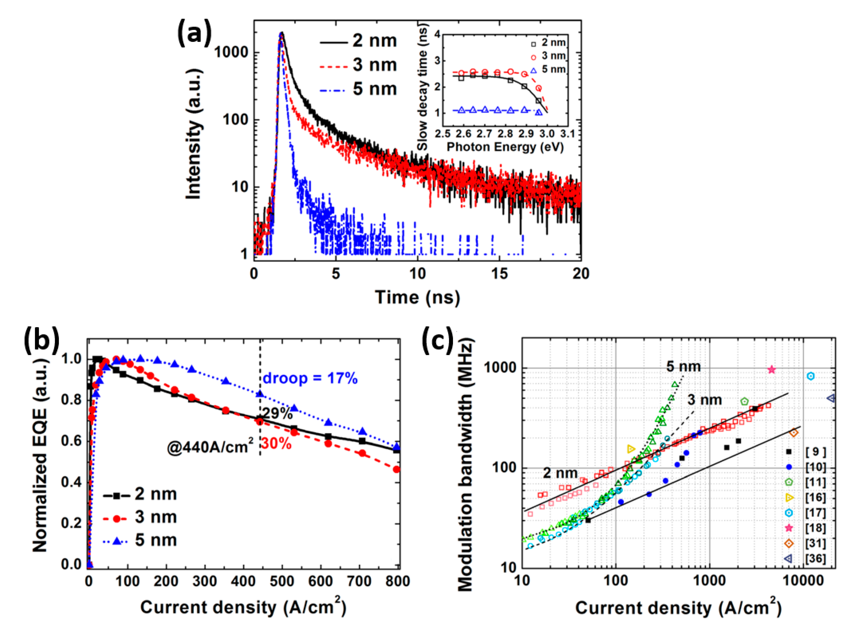
3.1. Quantum Confined Stark Effect and Carrier Localization Effect

In order to reach data transmission speeds of the order of Gb/s, the modulation bandwidth of LEDs for VLC applications needs to be substantially increased. There are two major factors affecting the modulation bandwidth of GaN-based LEDs: RC time constant and carrier lifetime in the active region [29]. An efficient way of reducing the RC time constant is to diminish the active region [30,31,32,33]. Several approaches have been suggested by decreasing the carrier lifetime, including reduction of active layer thickness [34], using a barrier-doped multiple quantum well (MQW) structure [29], using surface plasmon coupling [35], or using resonant cavity structures [36]. In addition, carrier lifetime can also be shortened by increasing the current density of the injection, thus increasing the bandwidth for the modulation [37]. However, increasing the current density may lead to reduction of the quantum efficiency and performance of LEDs [38]. The carrier lifetime is influenced by both the non-recombination lifetime τnr and recombination lifetime τr, and without affecting the luminous efficiency, a reliable way to improve the modulation bandwidth is to decrease the recombination lifetime [39]. The recombination lifetime is given by τr = 1/B(no + po + Δn), so in order to decrease the recombination lifetime, it is important to increase B to acknowledge the high speed of LED at a lower current density.
Several studies have revealed that the carrier recombination processes in GaN-based LEDs can be greatly affected by the effect of quantum confined Stark effect (QCSE) [40,41] and carrier localization [42,43,44]. To address this issue, Shichao Zhu et al. investigated the influence of the QSCE and carrier localization effect on the carrier lifetime by regulating QWs thickness [19]. Three GaN-based LED epilayers were developed using metal organic chemical vapor deposition (MOCVD) on c-axial sapphire (0001) substrates. The three epitaxial structures comprise of a 2 µm undoped GaN layer, a 2.3 µm Si-doped n-GaN layer, two sets of InGaN/GaN pre-wells, and five pairs of multiple quantum wells active with a 10 nm thick GaN quantum barrier, but with different thicknesses (2, 3, or 5 nm) of In0.1Ga0.9N QWs. Later, an electron-blocking layer of 40 nm thickness and a Mg-doped p-GaN layer of 150 nm thickness were deposited. LEDs with specific circular mesas and pixel diameters of 120, 90 and 60 μm were manufactured to validate whether the modulation bandwidth is constrained by the carrier lifetime. Figure 1a displays the time-resolved photoluminescence spectra (TRPL) at room temperature for LEDs with three different QWs of 2, 3, and 5 nm thicknesses. The LED with 2 nm QW thickness is found to have the longest carrier lifetime as compared to other LEDs with QW thicknesses of 3 and 5 nm. Since localized carriers are trapped within the QWs, they have a much longer decay time, and, hence, carrier lifetime can be correlated with the carrier localization effect in QWs. The carrier localization effect causes the carriers to be trapped within the QWs, and this effect inhibits the carriers from moving to non-radiative recombination centers, thereby increasing the carrier lifetime [43,44].
The slow decay times for the three LEDs have been extracted from the TRPL curves as a function of photon energy to reflect the degree of carrier localization, as shown in the inset in Figure 1a. The slow decay time is related to the depth of carrier localization, as shown in Equation (8).
τ s l o w ( E ) = τ 1 + exp [ E E m e E o ]
where τ is the carrier lifetime, Eo represents the depth of the carrier localization with the MWQs. The energy Eo for LEDs with QWs thickness of 2, 3, and 5 nm is derived using the experimental data to be 57, 29, and 3 meV, respectively. The optical power for LEDs with QW thickness of 2, 3, 5 nm has also been calculated. Due to the fact that thinner QW has a higher carrier density and more electron–hole wave functions are overlapped by QCSE, the optical power of 2 nm QW LED at a low current density is greater than that of 3 and 5 nm QW LED, resulting in an improvement in the radiative recombination rate and optical power. However, at higher current density of 3 nm QW LED has the largest optical power. The reduction of power in 2 nm QW LED at a high current density is due to Auger recombination and carrier overflow, but for 5 nm QW LED, the reduction can be explained with reduced carrier localization effects leading to Shockley–Read–Hall (SRH) recombination. Figure 1b displays the external quantum efficiency (EQE) for LEDs with different QW thickness. It can be seen from the figure that the efficiency droop effect for 5 nm QW LED is very small compared with 2 nm and 3 nm QW LEDs, which is consistent with the fact that 5 nm QW has a low carrier density in the individual QW, resulting in low Auger recombination or carrier overflow. Figure 1c describes the 3-dB modulation bandwidths for LEDs with different QW thicknesses of 2, 3 and 5 nm, and for certain QW thickness, the modulation bandwidths are almost similar at the same current density, suggesting that the modulation bandwidth is constrained by the carrier lifetime. To further confirm this, using Current-Voltage (I-V) and Capacitance-Voltage (C-V) characteristics, the RC-limited bandwidths have been calculated, i.e., 4111 MHz, 804 MHz, and 992 MHz for LEDs with 2 m, 3 nm, and 5 nm QW thickness, respectively. This calculated bandwidth is much larger than the optical modulation bandwidth and further confirms that the lifetime of the carrier is affecting the modulation bandwidth. It has been found that at 425 A/cm2, the modulation bandwidth for 5 nm QW LED reaches 700 MHz, which is much larger than that of 2 and 3 nm QW LEDs, and at such a low current density, it is also the highest modulation bandwidth. QCSE cannot explain this since the polarization field in this current density region has already become weak, as there is a decrease in the carrier localization effect, leading to an increase in carrier lifetime. As discussed above, the localization effect for 2 nm QW LED is the largest, but with increasing QW thickness, the localization effects decrease, which will reduce carrier lifetime and increase modulation bandwidth. It can be concluded that QSCE dominates the carrier recombination at lower current density, and, therefore, the rate of radiative recombination decreases. However, with an increase in current density, QSCE becomes less effective, thus increasing optical power and modulation bandwidth. In addition, weaker localization effects will result in a high bandwidth modulation.

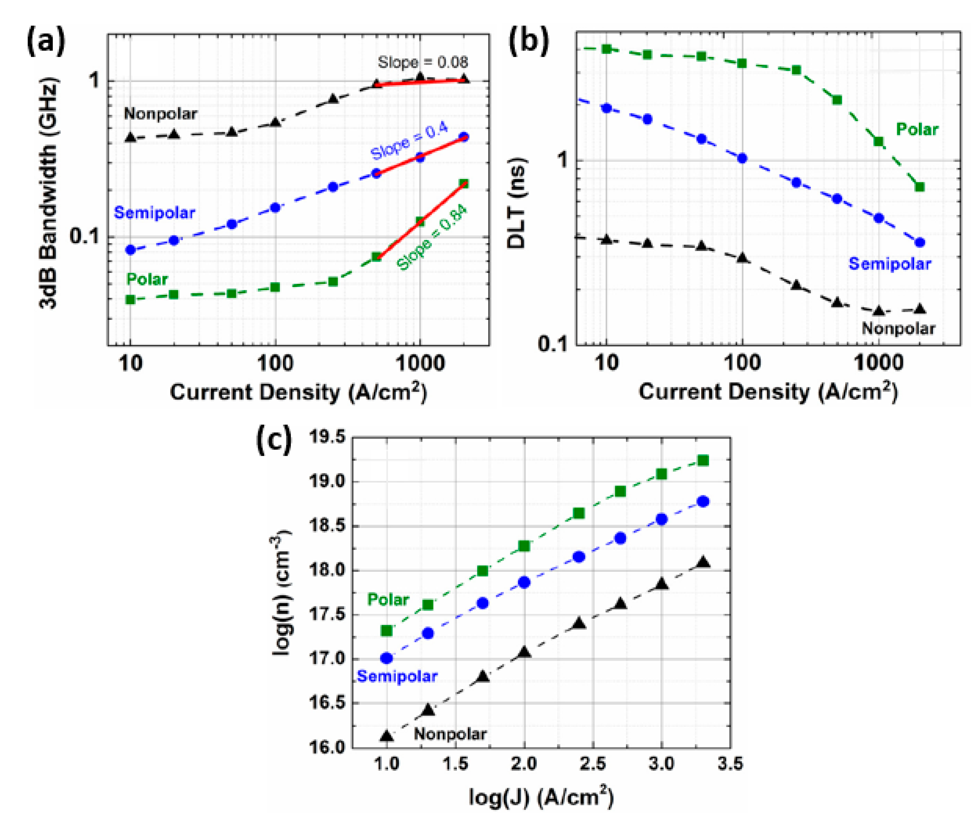
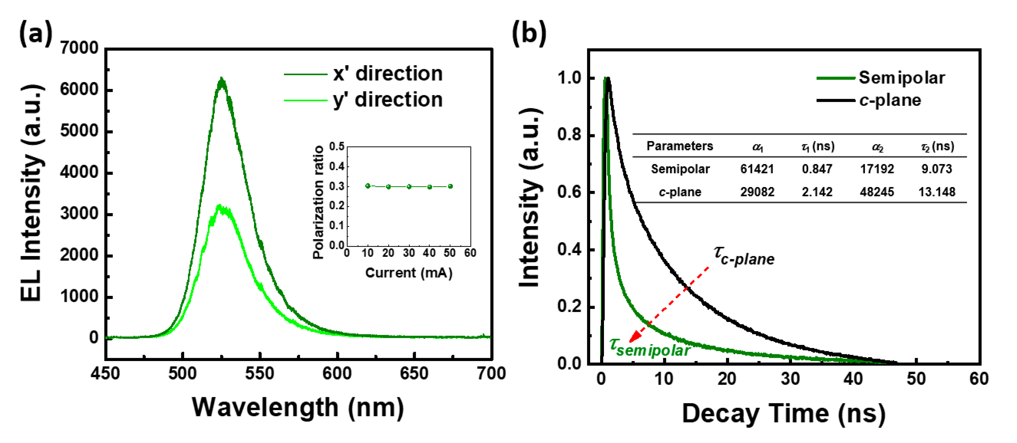
3.2. Crystal Orientation

Another important factor that can influence the modulation bandwidth of LEDs is the crystal orientation. For c-plane LEDs, which are polar, the carrier lifetime can only be reduced at higher current densities, thereby achieving a high modulation bandwidth. Operating at high current density, however, is unfavorable due to the efficiency droop effect [22,45,46], so finding a way to reduce the current density for a given modulation bandwidth and also to achieve higher quantity efficiency is necessary. Considering the nonpolar and semipolar LEDs, a higher modulation bandwidth can be achieved at lower current density due to the larger overlap of the electron–hole wave function and shorter carrier lifetimes [25,26,47,48,49]. However, due to the higher ratio of radiative-to-Auger recombination coefficients, there is an efficiency droop problem for certain semipolar orientation, like (20-2-1) [50].
M. Monavarian et al. measured modulation bandwidths for different InGaN/GaN μ-LEDs with a QW thickness of 4 nm, 4 nm, and 6 nm for the polar, semipolar, and nonpolar structures in order to compare the modulation responses [51]. Figure 2a describes the 3 dB modulation bandwidth as a function of current density for the polar, semipolar, and nonpolar μ-LEDs. The nonpolar LED obviously has the highest modulation bandwidth of ~1 GHz at a low current density of 500 A/cm2 followed by the semipolar device and then by the polar device. The overlap of the electron–hole wave function will seriously affect the modulation bandwidth, as both radiative and non-radiative recombination rates depend on the overlap of the wave function that links to the speed. Since the average wave function overlap in the nonpolar QWs is around 3 to 8 times higher than that of polar QWs, the bandwidth is higher in the case of the nonpolar device. However, with an increase in the current density, the bandwidth of the polar LED increases at a faster rate compared to the semipolar and nonpolar LEDs due to the coulomb screening effect [19]. Figure 2b gives the differential carrier lifetimes (DLTs) for the three orientations as a function of current density using the relation. The DLTs can be calculated using the relation τΔn = 1/(2πf3dB), where τΔn is the DLT. The carrier density can be calculated using n = 0 G τ Δ n   d G   , where n is the carrier density and G is the generation rate, which can be calculated from the relation G = J/(e × d), where J is the current density, e is the electron charge, and d is the active layer thickness [50,52,53]. Using the data from Figure 2a, the approximate Shockley–Hall–Read (SHR) lifetimes have been extracted and found to be 0.4 ns for nonpolar, which is shorter than that of semipolar (2.0 ns) and polar (4.0 ns). At higher current densities, due to Coulomb screening of the polarization field, the DLT for the polar device decreases at a faster rate compared to the nonpolar and semipolar devices. The carrier density was calculated, and it was found that in the case of nonpolar, the current density is lower for a given current density followed by semipolar and then by polar, as shown in Figure 2c. This trend can be explained by the greater electron–hole wave function overlaps in nonpolar and semipolar, resulting in higher recombination rates [54]. Thus, the bandwidth of nonpolar and semipolar LEDs at low current density is higher than that of c-plane LEDs, and it can also operate more efficiently due to reduced drop in efficiency.

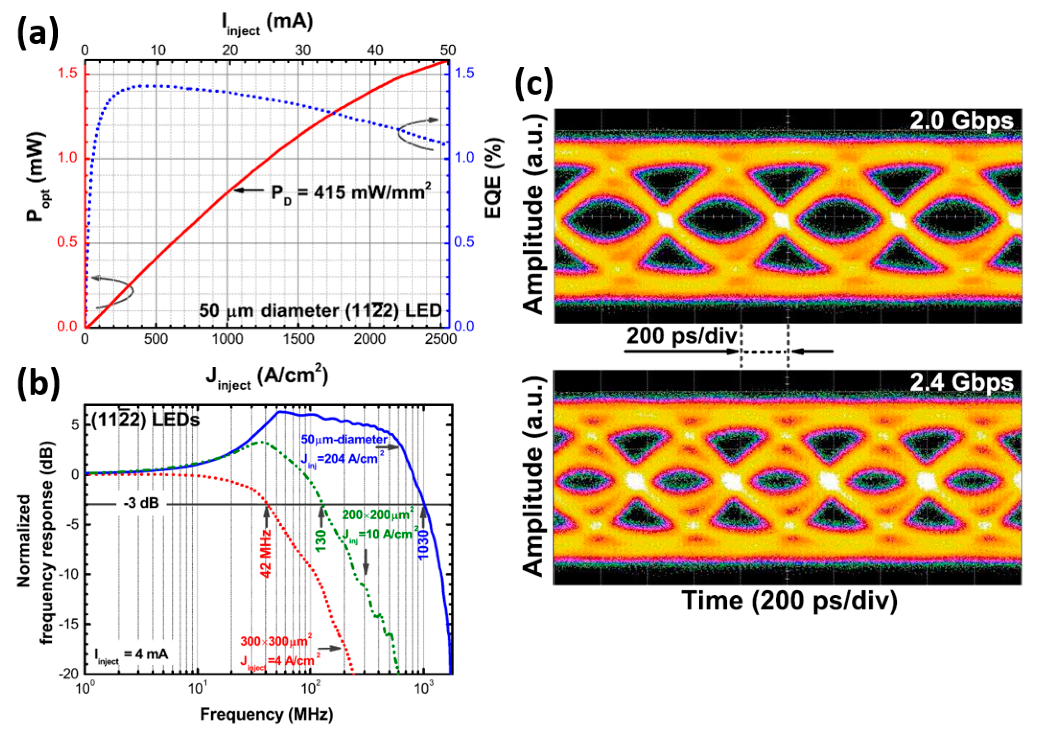
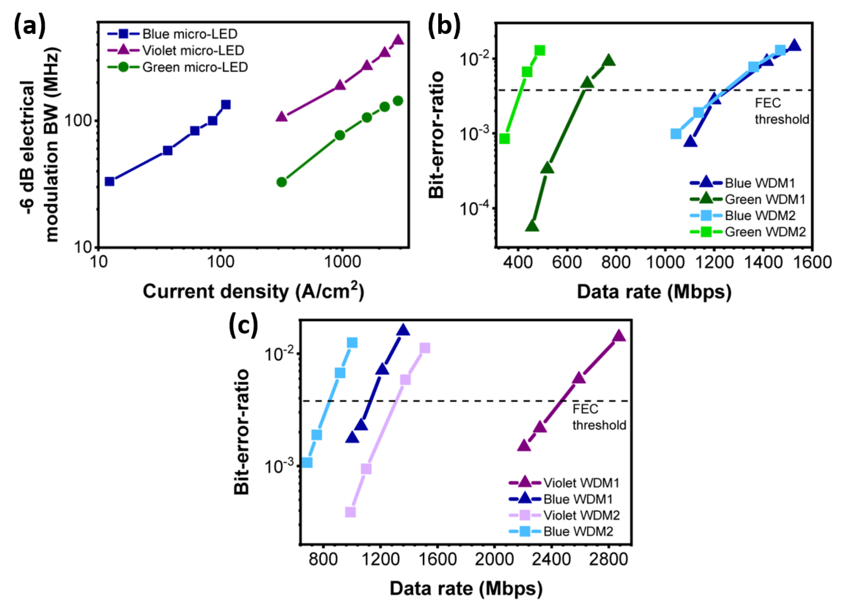
4. Semipolar LED-Based VLC Applications

As mentioned in the above section, conventional c-plane LEDs suffer from strong spontaneous and piezoelectric polarization, leading to performance issues, and their modulation bandwidth is limited by the carrier lifetime and the parasitic capacitance. These polarization-related problems may be prevented in nonpolar and semipolar LEDs, but due to the planar anisotropic nature of the growth mode, it is difficult to produce high-quality nonpolar material [55]. In addition, nonpolar planes often suffer from poor surface morphology that prevailed over a wide range of growth conditions compared to semipolar planes that offer better crystallinity, resulting in faster transit response of the device [56]. Several papers have stated that the polarization-related electric fields for semipolar InGaN QWs can be substantially lowered, resulting in a reduced carrier lifetime. However, few studies have been conducted regarding its potential applications in terms of visible light communications. As mentioned in the above section, the modulation bandwidth is limited by QCSE, and to overcome this, researchers need to grow nonpolar structures on bulk GaN.
As a part of this, Dinh et al. demonstrated blue emitting semipolar (11-22) InGaN/GaN LEDs with the measured frequency response at -3dB reaching 1 GHz and a back-to-back data transmission rate of over 2.4 Gbps [57]. The LED structure is composed of three- or five-period InGaN/GaN QW active layers, Si-doped n-type GaN of 1.5 µm thickness, n-type In0.01Ga0.99N of 100 nm thickness, 120 nm thick Mg-doped p-type GaN, and a heavily doped p-type GaN contact layer with a thickness of 15 nm. For this study, three LED configurations were made, namely, non-mesa-etched µ-LED with Pd-contacts and a 50 µm diameter, and 200 × 200 and 300 × 300 µm2 macro-LEDs with Ni/Au contacts. The output power of the semipolar LED is represented by the red curve in Figure 3a and is estimated at a current density of 1020 A/cm2 to be about 0.81 mW with an optical power density of 415 mW/mm2. The external quantum efficiency (EQE) of the semipolar LED is shown by the blue dotted line in Figure 3a, reaching a maximum value of 1.4% corresponding to an injection current density of 510 A/cm2. The EQE decreases slowly up to 1.1% when the injection current density increases to 2500 A/cm2. This efficiency droop in this (11-22) LED can be explained by various factors related to heat generation and current crowding [58]. This small efficiency droop in semipolar LEDs can prevent problems related to data transmission for VLC systems such as reduction in the transmission signal, which can be significantly found in (0001) LED-based systems. The frequency response of the semipolar (11-22) LEDs with different sizes, such as a non-mesa-etched 50 µm diameter, 200 × 200 µm2, and 300 × 300 µm2, at different injection current density are shown in Figure 3b. The frequency response at -3dB is found to increase from 42 MHz to 1030 MHz, with injection current density increasing from 4 A/cm2 to 204 A/cm2. The 50 µm diameter LED has the highest frequency response of 1030 MHz at the injection current density of 204 A/cm2. These values of frequency response are higher than that of conventional (0001) LEDs, which can be attributed to the shorter recombination lifetime due to the reduced polarization-dependent electric fields in the semipolar (11-22) QW structures. The data transmission rates for the (11-22) LEDs are also evaluated to demonstrate that they can clearly be used for data transmission. A digital oscilloscope (Agilent Infiniium DSO80804A) collected the large signal properties/back-to-back data transmission rates of the LEDs. It is found that the transmission rate for the non-mesa-etched 50-µm diameter LED reaches over 2.4 Gbps when a 2 V peak-to-peak amplitude is applied at an injection current greater than 10 mA. Figure 3c shows the eye diagram for the non-mesa-etched 50 µm diameter LED at 2.0 and 2.4 Gbps when biased at 10 mA. For 300 × 300 µm2 LEDs, the transmission rate is found to surpass 600 Mbps at an injection current of 50 mA, and these high speeds and data rates of (11-22) LEDs suggest that they can be used as photodetectors in the visible range. However, data communication rates can be made even faster for semipolar (11-22) LEDs by using higher-level encoding methods that have already been demonstrated in conventional (0001) LEDs, achieving transmission rates of up to 5 Gbps.
However, when it comes to white light VLC applications using blue LEDs, many challenges come into existence, such as poor efficiency, stability issues, color rendering problems, etc. Thus, the ultimate solution is to develop the RGB light emission for obtaining white LEDs, but still there are some challenges in terms of optical performance for green emitting LEDs. In this regards, Haggar et al. demonstrate semipolar (11-22) green InGaN/GaN LEDs by achieving a modulation bandwidth of 540 MHz at an injected current density of 92 A/cm2 [59]. This give a clear picture about the suppression of the polarization-related electric field in semipolar LEDs, however, with an increase in In content, the polarization for the semipolar LEDs will increase, which will affect the device performance. It is found that the modulation bandwidth of the semipolar LED increases with the increase in injection current density, implying that the modulation bandwidth is not restricted by the junction capacitance and the 3 dB bandwidth can be further improved beyond this value. The high modulation bandwidth of this semipolar device is attributed to shorter carrier lifetime (0.31 ns), which has been extracted from the time-resolved photoluminescence (TRPL) measurement. This value is the record modulation bandwidth for GaN-based macro-LEDs.
There is another recent improvement in the modulation bandwidth for green emitting LEDs from Chen et al. by demonstrating green semipolar (20-21) InGaN/GaN μ-LEDs with a high bandwidth for visible light communication [60]. The structure of the LED comprised of three pairs of InGaN/GaN MQWs as the active region, n-type GaN having a thickness of 1.5 μm and a 100 nm thick p-type layer. The LED structure process flow started with the deposition of semipolar (20-12) GaN on patterned sapphire substrate (PSS) using a low-pressure chemical vapor deposition (MOCVD). Figure 4a demonstrates the μ-LED device structure optimized to achieve high performance in VLC applications by means of different designs. To obtain a low RC time constant, the LED’s electrode has been optimized to suppress the capacitance. The active region and the electrode have been designed in a circular manner to enhance the current spreading and increase the electrical efficiency. To remove the effect of sidewall defects from the etching process, an Al2O3 layer deposited by the atomic layer deposition (ALD) is employed. The DBR at the back of the LED is used to improve the device’s output power. Figure 4b represents the electroluminescence (EL) spectra of the semipolar (20-21) µ-LEDs with an increasing injection current from 5 mA to 50 mA, and the inset in Figure 4b displays the photograph of the device at a current of 10 mA. The EL spectra show a 14.9 nm wavelength shift, which becomes stable after an injection current of 50 mA, indicating a good performance. This wavelength shift is attributed to strong QCSE in the semipolar µ-LEDs resulting from the reduced polarization-related electric field, leading to an increase in the QW band gap. The FWHM for the emission peaks shows a slight change of only 3 nm from 5 to 50 mA, suggesting a low defect density and good uniformity in the structure of the device. Figure 4c shows the relationship between the current density (J) and the voltage (V) in the forward voltage, while the inset gives the Current density-Voltage (J–V) relation at reverse voltage used to evaluate the leakage current. The device has a 2.2 V turn-on voltage that can be considered good performance for the green μ-LEDs, but the device shows a high resistance that could be due to reverse polarization or weak ohmic contact in the p-type region. However, this resistance will not affect the 3-dB bandwidth for VLC device application because µ-LEDs have extremely small capacitance. The inset curve shows that the device has a low leakage current density of about 10−6 A/cm2, which may be due the passivation layer formed by the ALD process and low defect density in the semipolar GaN. As the chip size gets smaller, the sidewall effects and surface recombination can lead to leakage, and, from this result, the passivation effect is believed to be important to avoid such problems.
The EL spectra of the semipolar µ-LED using a polarizer are measured as shown in Figure 5a. The two EL spectra correspond to the polarizer directions along (1-210) and (10-1-4) defined as x‘-and y‘-directions, respectively. The x‘- and y‘-direction correspond to the maximum and the minimum intensity of the emitted light through the polarizer. Using these values, the polarization ratio of the semipolar µ-LED is calculated and found to be 0.3, corresponding to injection current of 50 mA. The polarization ratio as a function of the injection current is shown in the inset in Figure 5a, indicating that the polarization is independent of the injection current. The characteristics of polarization can be useful when it comes to data transmission more efficiently, as polarization-multiplexing technology can be used to exploit light polarization and help to improve the rate of transmission [61]. Figure 5b displays the TRPL measurement for semipolar (20-21) µ-LED and the commercial c-plane µ-LED performed at low power of 20 µW. Some important parameters have been extracted from the fitting curves, such as decay lifetime, τ and fractions of electron–hole pairs, α. The lifetime of the minority carrier for semipolar and c-plane μ-LEDs has been estimated using these parameters, and found to be 2.65 and 9.00 ns, respectively. Due to low polarization-related electrical fields and greater overlap of the electron–hole wave function, the semipolar μ-LED has a shorter lifetime than that of c-plane μ-LED. Hence, it would result in faster carrier recombination for semipolar LEDs and, correspondingly, a higher frequency bandwidth.
The frequency response of the semipolar (20-21) µ-LED at -3 dB for different injection current is shown in Figure 6a. It is found that the bandwidth increases with the increase in the injection current density owing to the reduced built-in electric field and shortened carrier lifetime at a higher injected current density in the active region. The μ-LED’s highest 3-dB bandwidth reaches up to 756 MHz, which corresponds to an injected 40 mA current. Clearly, the 3-dB bandwidth is proportional to the increasing current density, indicating that the bandwidth is not limited by the RC delay but the carrier recombination lifetime. Figure 6b shows the eye diagram for the semipolar μ-LED at 40 mA, and the eye diagrams are fairly clear and open at 1.0 and 1.5 Gbps, but the eye region is not apparent when the data rate reaches 2 Gbps due to the relatively low signal-to-noise ratio. In addition, various researchers reported different modulation bandwidth for semipolar LEDs. In 2016, Corbett et al. showed green semipolar LEDs with a 100 MHz bandwidth under a 30 mA injection current. Khoury et al. demonstrated white semipolar LEDs with a 20 μm diameter chip showing a 660 MHz bandwidth in 2020. A comparison has been made based on the existing device performance for a semipolar LED-based VLC system, as shown in Table 1.

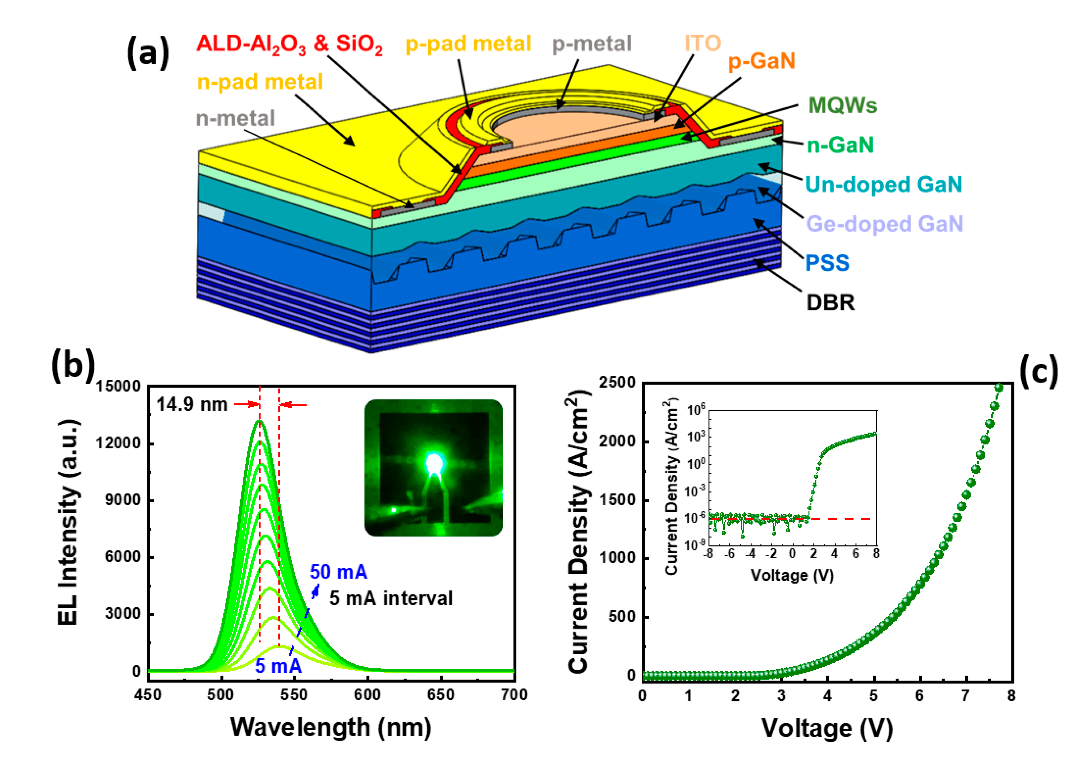
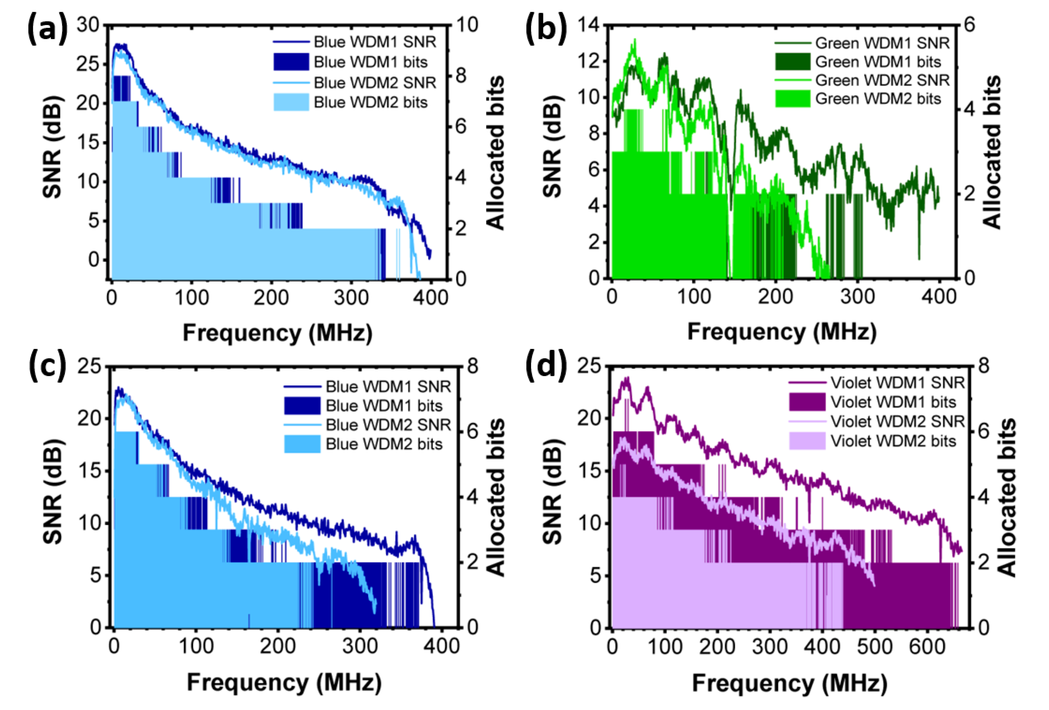
5. Micro-LED Array-Based VLC

As discussed in the earlier sections, µ-LEDs exhibit potential for numerous applications, including VLC which is yet to be fully explored [66,67]. The usefulness of GaN-based µ-LEDs is due to their exceptional performance in terms of high brightness, high contrast, rapid response time, extended operational lifetime, and reduced power utilization [68]. Assemblies of µ-LEDs, containing a large number of µ-LED components, are usually referred as µ-LED arrays. Optical power given out by a single µ-LED is quite low due to its ultra-small emitting area. Output optical power can be enhanced by making use of many µ-LED components assembled as an array. µ-LED arrays can be prepared with both single- and multi-color emission [68,69]. Multi-color µ-LED arrays are quite common in research circles due to the fact that they have widespread scope of application in display technology [70,71]. In the previous sections, we have discussed applications of only single LED or µ-LED elements in VLC technology. In this section, we review works reporting the application of µ-LED arrays in the field of VLC. Many applications, including visible light communication (VLC), demand for integration of multi-color emitters on a single chip, which can be realized by combining blue µ-LEDs with a color-converting substance (called phosphor), thus facilitating down-conversion of the shorter emission wavelengths to longer ones. Color down-converters are not feasible for many applications owing to their lower efficiency, shorter operational lifetime and slower response time [72]. A solution to this issue is to grow blue, green and red emitters on materials, which suit them and consequently transfer them on a single, shared substrate. Traditional robotic system-based transfer techniques cannot be used to assemble µ-LEDs as these techniques are not capable of handling micro-sized dices [73]. An alternative solution is the use of transfer printing along with the techniques to suspend releasable thin µ-LED components [74]. VLC transmitters based on single wavelength GaN µ-LEDs have been reported in the literature with multi-Gbps transmitting capacity [75,76]. However, single chip µ-LED arrays with multi-color emission have not been explored as VLC transmitters extensively.
As a part of µ-LEDs array for VLC applications, Carreira et al. [77] reported transfer printing-enabled on-chip GaN-based blue-green and blue-violet micro-LED arrays. In the work put forward by Carreira et al. [77], there is fabrication of dual-color µ-LED arrays by combining blue µ-LED platelets with violet and green µ-LEDs through transfer printing. The optical characteristics of the µ-LEDs for VLC application have been analyzed in the following section. The -6 dB electrical modulation bandwidths of violet, green and blue µ-LEDs are measured and found to be 427 MHz, 144 MHz and 134 MHz, respectively, as shown in Figure 7a. Low bandwidth of green µ-LED is a consequence of higher ratio of indium content in the active area, which gives rise to a stronger quantum confined Stark effect [78]. The lower bandwidth of blue µ-LED is attributed to its larger pixel size and, which consequently results in low current density action. Both sets of µ-LED arrays (i.e., blue-violet and blue-green arrays) have the capacity to operate as visible light communication (VLC) transmitters in two different set-ups named wavelength division multiplexing (WDM)1 and WDM2, and the details of which can be found in [77]. In the first set-up, i.e., WDM1, two different streams of input signals are sent using µ-LED channels where one of them is received and demodulated by the optical receiver, and the other simply acts as an interference signal. In the second scheme called WDM2, light from the µ-LED arrays is focused to two dichroic mirrors at an angle of 45 degrees, and the mirrors split the input beam into two separate parts by transmitting one portion of it and by reflecting the other portion. The WDM2 scheme makes it possible to receive signals from both the channels at the same time, though dichroic mirrors cause some power loss to the input signal as a tradeoff. Some characteristic parameters of a communication system like BER, signal-to-noise ratio (SNR), and data rate are calculated for this set-up.
The BERs for the blue and green µ-LEDs system as well as blue and violet µ-LEDs system in both WDM set-ups are plotted as a function of the data transmission rate, as shown in Figure 7b,c. In the WDM1 configuration, below the forward error correction (FEC) threshold, the blue and green µ-LEDs will achieve a maximum data rate of 1261 and 667 Mbps, respectively. The maximum data rates for blue and green µ-LEDS below the FEC threshold decreased to 1245 and 410 Mbps, respectively, in the WDM2 configuration. Similarly, for the blue and violet µ-LEDs, the maximum data rate in the WDM1 set-up can reach up to 1130 and 2472 Mbps, respectively, below FEC threshold, while their maximum data rates below FEC threshold in the WDM2 set-up decrease to 842 and 1309 Mbps, respectively. Figure 8 display the SNR for blue-green µ-LED array as well as blue-violet µ-LED array in both WDM set-ups at the highest rate. It can be seen from Figure 8a,b that the blue µ-LED channel shows a higher SNR as compared to the green µ-LED channel due to its higher optical power. Moreover, the SNR curves for the blue channel in both WDM set-ups shows a similar nature, however, the SNR curve for the green channel in WDM2 drops severely when the frequency exceeds 150 MHz as compared to that of the WDM1 set-up, which is attributed to optical power loss of about 25 % resulting from the dichroic mirror used in the WDM2 set-up. However, when it comes to the blue and violet µ-LED channels, as shown in Figure 8c,d, the SNRs curves for both channels are quite similar because of comparable optical power. Like blue-green transmitters, SNR values for blue-violet µ-LED arrays are observed to be well above the FEC threshold. The violet µ-LED can achieve bit allocation until 650 MHz, however, it still suffers from optical power loss of about 11 % because of the dichroic mirror. In addition, it is possible to technically incorporate the two dual-color micro-LED arrays into the same package to provide a three-color output that will open a way in terms of WDM VLC connections.
In another study related to µ-LED array for VLC application, Xie et al. [79] report fabrication and characterization of blue-only nitride µ-LED arrays with series-biasing and demonstrate their application in VLC. The μ-LED array reported in this experiment contains flip-chip configured μ-LED components arranged in the form of a 3 × 3 μ-LED matrix where every component has an emissive area of 1256 µm2 and a diameter of 40 µm. The μ-LED array presented in this report has the benefit of the fact that light-emitting devices working at high driving current densities have a shorter differential carrier lifetime and consequently an enhanced value of modulation bandwidth. The 6-dB electrical bandwidth of the demonstrated μ-LED array comes out to be more than 280 MHz when driven at a current density value of 3200 A/cm2, as shown in Figure 9a. It is noted that the collective optical power of an μ-LED array with nine components is a bit less than nine times the optical power given out by an individual μ-LED component of the same size and operating under the same condition [75]. The literature suggests that absorption of light among adjacent components and thermal effects are responsible for this phenomenon [80]. The joint modulation bandwidth of the μ-LED array, on the other hand, is more than the expected value suggested by the bandwidth of a single component driven at the similar conditions. This happens because series biasing of μ-LED components leads to a lower capacitance, as reported in [81]. The details of this experimental set-up can be found in [79]. The free-space VLC implementation for this series-biased µ-LED array has been demonstrated with On-off keying (OOK), Pulse Amplitude Modulation (PAM), and Orthogonal Frequency-Division Multiplexing (OFDM) modulation formats.
A comparison between eye diagrams of the transmitted and received signals is presented in Figure 9b,c where the OOK modulation scheme is adopted at a bit rate of 700 Mbps and the reported μ-LED array is used as a transmitter. It can be observed that the amplitude and temporal distortions created by the channel are easily observable at a comparatively low bit rate used in the experiment. These distortions lead to undesirably high BERs by introducing inter symbol interference. To address this issue, a finite impulse response filter is used as a feedforward equalizer. The equalizer used in the experiment minimizes non-uniformity of the received symbols before this equalizer, which is a consequence of Intersymbol Interference (ISI) as reported in [82]. The equalizer used in the experiment keeps received symbols below a specific decision threshold, which keeps the spread of the received symbols relatively narrower and ultimately lowers the BER.
The SNR for the µ-LED for OFDM modulation format is shown in Figure 10a as a function of bandwidth. High SNR ensures a high probability of the transmitted signal being distinguished by the decoder. The reported μ-LED array transmitter maintains SNR values over 10 dB up to a bandwidth of 1.2 GHz, which shows the potential of high-speed data transmission capability. As evident from Figure 10b, the maximum data rate offered by the reported μ-LED array-based transmitter under 4-PAM and OFDM modulating is 2.55 and 5.18 Gbps, respectively, while meeting the FEC condition of 3.8 × 10⁻³. After implementing 7% FEC overhead reduction, the error-free data rates offered under OOK, 4-PAM and OFDM format turn out to be 1.95, 2.37 and 4.81 Gbps, respectively. A new form of VLC applications other than data transmission in the free space is the underwater communication, which will be described in the following section.

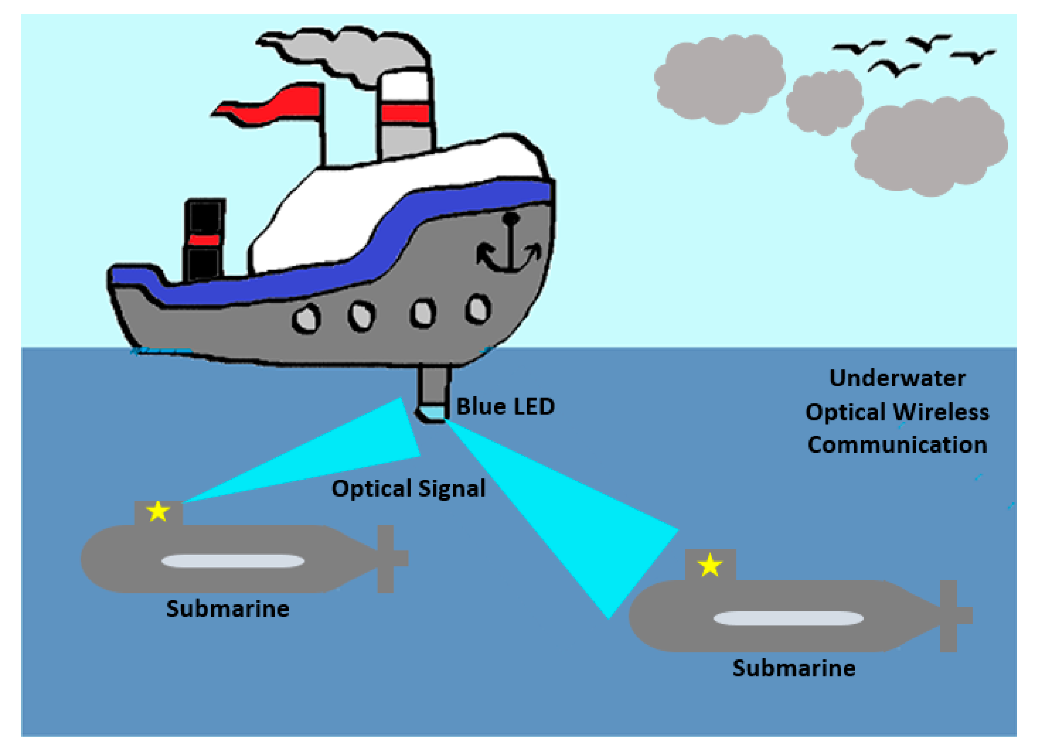
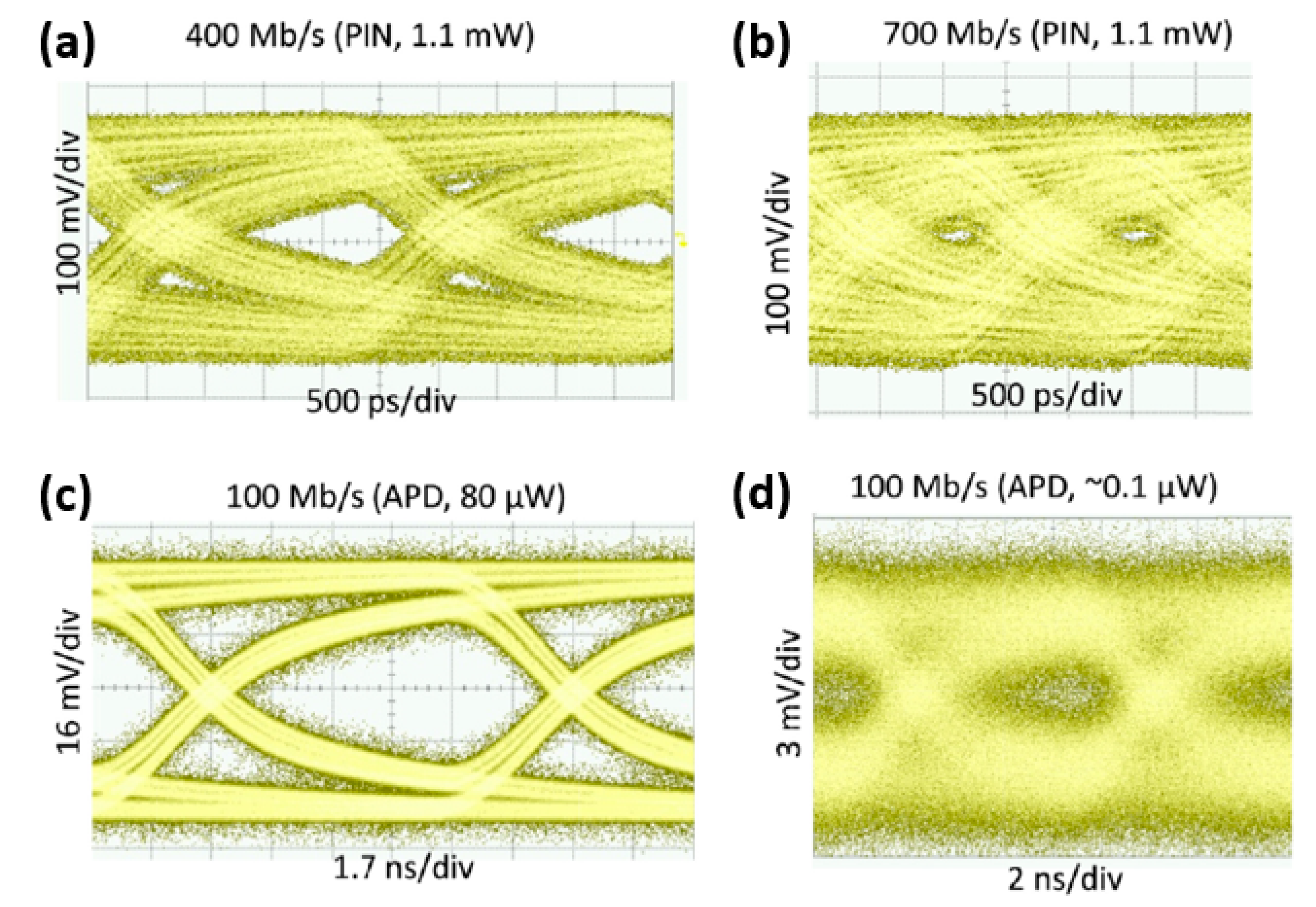
6. Underwater Optical Wireless Communication

Underwater communication (UC) has received significant interest as part of the VLC applications due to growing ocean exploration demands, and researchers are making substantial efforts into realizing UC systems with a longer distance, a higher transmission rate and lower BER [83,84]. Sonar has been commonly used for this UC application but suffers from a low transmission rate and latency, while using RF for UC is limited with a short range and high cost [85]. UOWC has therefore been introduced and is an innovative technology with numerous advantages, such as high speed, low latency, low cost of implementation and high safety [85]. LEDs and laser diodes have been commonly used as the light source for the UOWC systems, however, the transmission distance is short for the commercial LEDs and it has a limited bandwidth, making it difficult to maintain a high data transmission rate. μ-LEDs based on III-nitride semiconductors such as GaN offer efficient solution to address the restricted bandwidth issue by displaying low RC delay [86,87]. However, due to low output power, μ-LEDs are not preferable for high attenuation UOWC, but despite having a small bandwidth, they display tremendous potential in UOWC for medium/short distance transmission. An overview of UOWC is shown in Figure 11.
Recently, Wei et al. demonstrated 2 Gbps/3 m air-underwater optical wireless communication using a single-layer quantum dot (QD) blue µ-LED [88]. The QD µ-LED structure consists of 75µm single-layer InGaN QDs as the active region and SiO2 as the passivation layer. The indium tin oxide (ITO) layer is deposited on the top of QD µ-LED to form ohmic contact. The passivation layer is used to reduce the current leakage and enhance the output optical power. The experimental set-up for the QD µ-LED-based UOWC system uses 1 m free space and 2 m underwater distance. A BER tester (BERT Anritsu MP2100A) is used to evaluate the communication efficiency by generating pseudo-random binary signals (PRBSs) with non-return-to-zero (NRZ)-OOK modulation format. The NRZ-OOK signals are transmitted through an amplifier until the bias-tee superimposes them with the direct current (DC). The superimposed RF and DC signal then drives the micro-LED with the bias tee and activates the modulated light. Using a convex lens, the optical light is focused and then transformed into an electrical digital baseband signal that is further amplified by an amplifier. The transmitted signal first feeds back to the BERT to record the eye-diagram using the digital sampling oscilloscope and measure the system’s BER using the BERT error detector at various data transmission rates. The modulation bandwidth has been calculated and found to increase with increasing current density, and it even reaches 1.03 GHz corresponding to a current density of 582.54 A/cm2, which is a record-breaking bandwidth with such a short-range UOWC system. The eye-diagram of the device set-up becomes unclear when the data rates are 1.6 and 1.8 Gbps corresponding to BERs of 2.14 × 10⁻⁴ and 4.20 × 10⁻⁴, respectively. The eye-diagram is nearly closed at 2.0 Gbps corresponding to BER of 2.03 × 10⁻³, but the highest data rate of 2.0 Gbps is achieved under the forward error correction (FEC) criterion of 3.8 × 10⁻³. This is the highest data rate record for the UOWC system based on a single-layer QD μ-LED with a 3 m air–underwater transmission distance.
In another research by Tian et al., there is demonstration of an 80 µm blue-emitting micro-LED for high-speed underwater optical wireless communication [89]. As mentioned in the above section, underwater optical communication suffers from water absorption, scattering from suspended particles, etc., however, water attenuation is relatively small in the blue-green spectrum region, thus making blue or green emitting LEDs suitable for UOWC. In the work carried out by Tian et al., GaN-based micro-LED array emitting blue light has been manufactured on sapphire substrate, and the LED structure consists of InGaN/GaN MQWs, which is then bonded to a printed circuit board (PCB). The packaged micro-LED array is then tested for underwater communication by analyzing the characteristics of the transmitted light after passing through a water tank. The micro-LED has been driven by a DC bias to measure the -3 dB electrical-to-optical bandwidth using a network analyzer. The frequency response of the micro-LED is shown in Figure 12a for different injection currents ranging from 1 mA to 88 mA, and the extracted -3dB modulation bandwidth is shown in Figure 12b as a function of the injection current. It is clear from that the bandwidth initially increases up to 160 MHz and then remains constant from 61 mA. The BER has been analyzed at different injection currents from 16 mA to 88 mA, as shown in Figure 12c. It is found that high transmission speed can be achieved at a higher injection current, which is attributed to the increase in modulation bandwidth and light output power. A BER of 1.3 × 10⁻³ is obtained at 88 mA with a data rate of 800 Mbps, and the data rate is limited from the saturation of the modulation bandwidth at 61 mA. However, the data rate can be further improved by using an OFDM modulation scheme, which allows different modulation schemes for UOWC.
The obtained light output power at a fixed driving current for UOWC application is the key limiting factor due to the heavy attenuation of power. The BER is again analyzed with respect to the received light output power by maintaining at an injection current of 61 mA. A higher current, i.e., 88 mA, can be used to drive the micro-LED to evaluate the BER and obtain a more efficient value, however, a high injection current may hinder the reliability of the micro-LED. It is observed from Figure 12d and the inset figure that a data rate of 100 Mbps is achieved at received light powers of 80 µW and 0.1 µW using p-i-n (PIN) and Avalanche Photodiode (APD) receivers, respectively. The system offers the ability to achieve a data transmission speed of 100 Mbps at distances of about 11 m with a PIN receiver and about 40 m with an APD receiver. The eye diagrams for the micro-LED at 400 Mb/s and 700 Mb/s using a PIN photodetector receiver are shown in Figure 13a,b, and one open diagram can be seen in Figure 13a, implying free error data transmission. The closed eye diagram in Figure 13b corresponds to a BER of 4.8 × 10⁻⁷. Using the APD receiver, the eye diagram is open for received output power of 80 µW, as shown in Figure 13c, indicating free error data transmission, and the eye diagram is almost closed in Figure 13d, corresponding to output power of 0.1 µW.

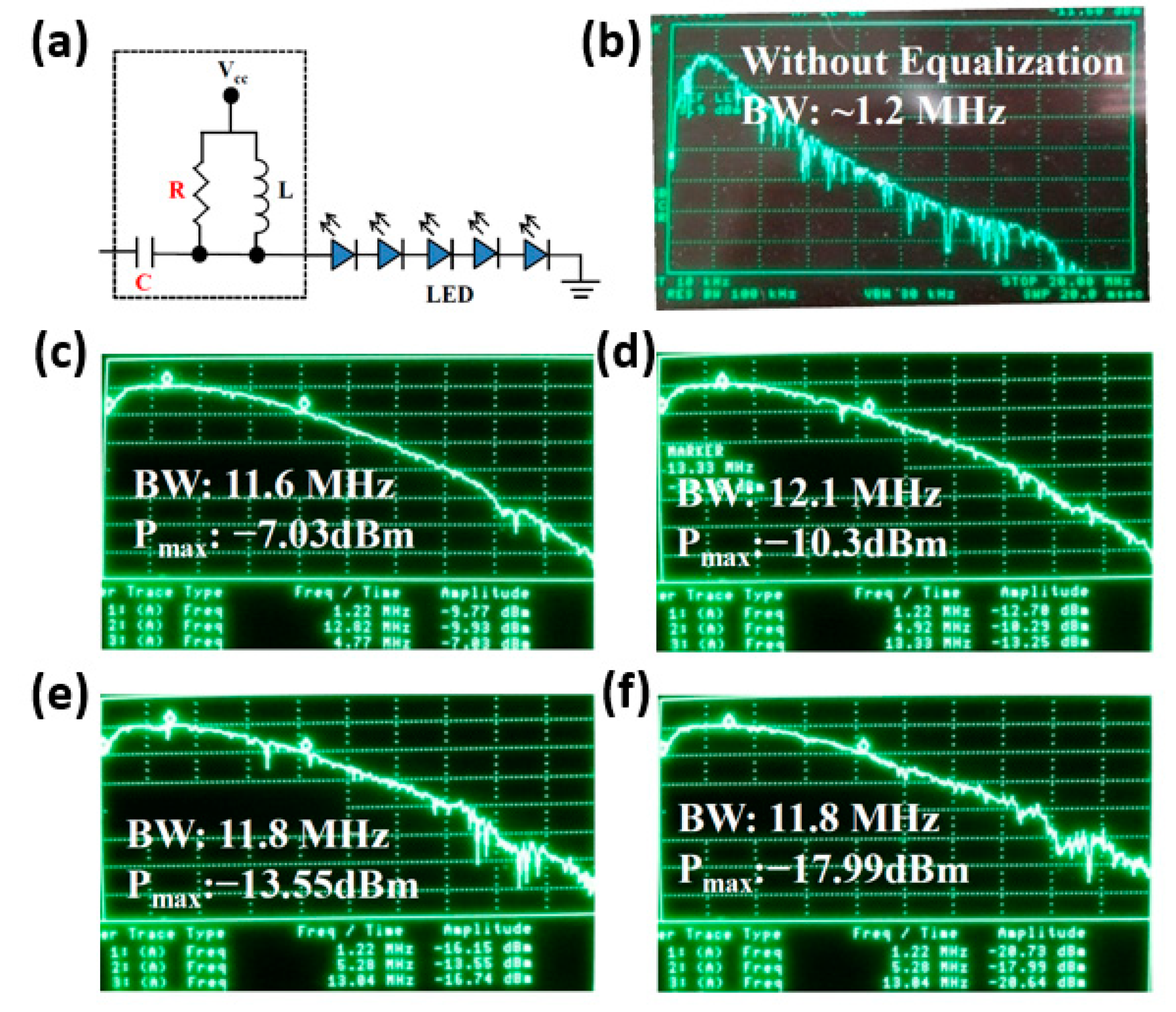
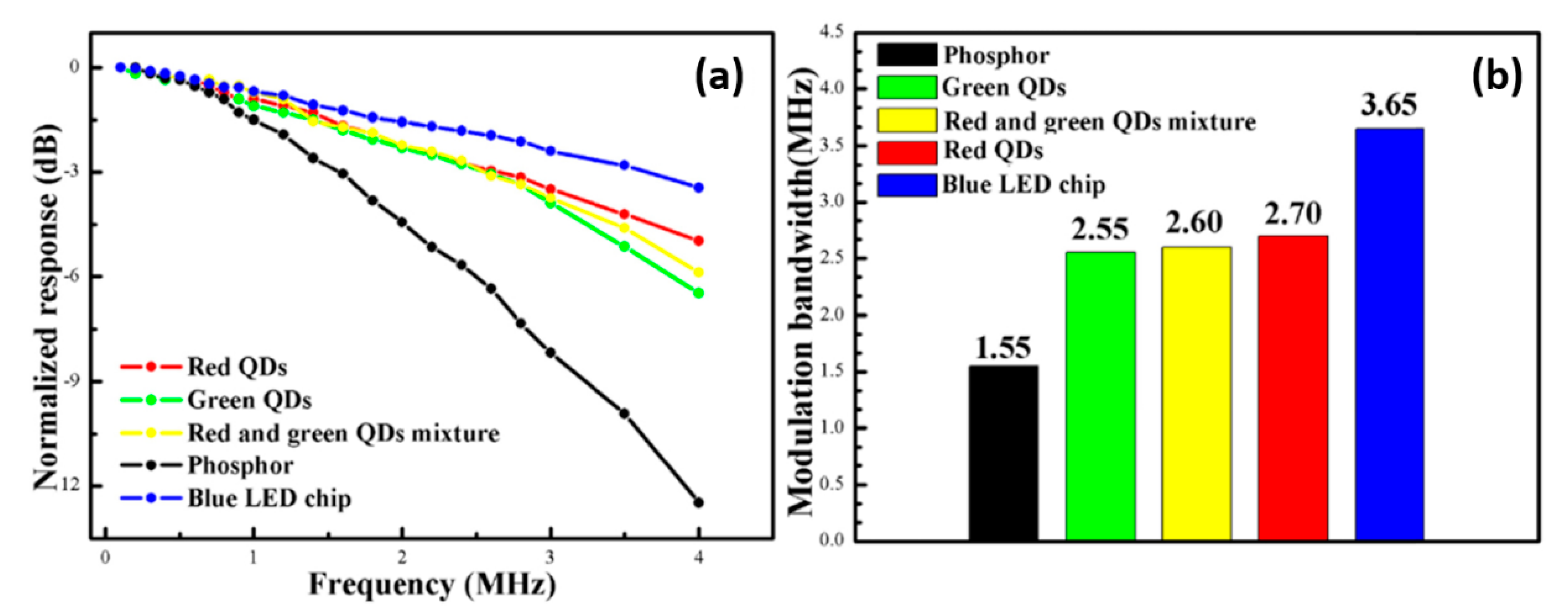
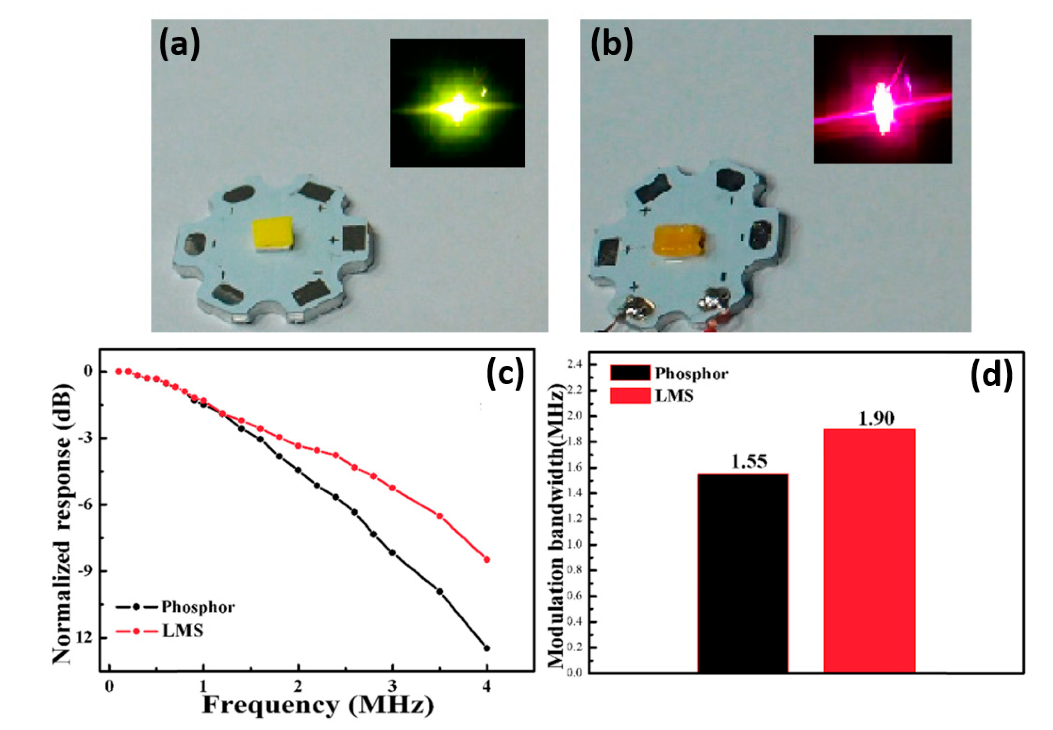
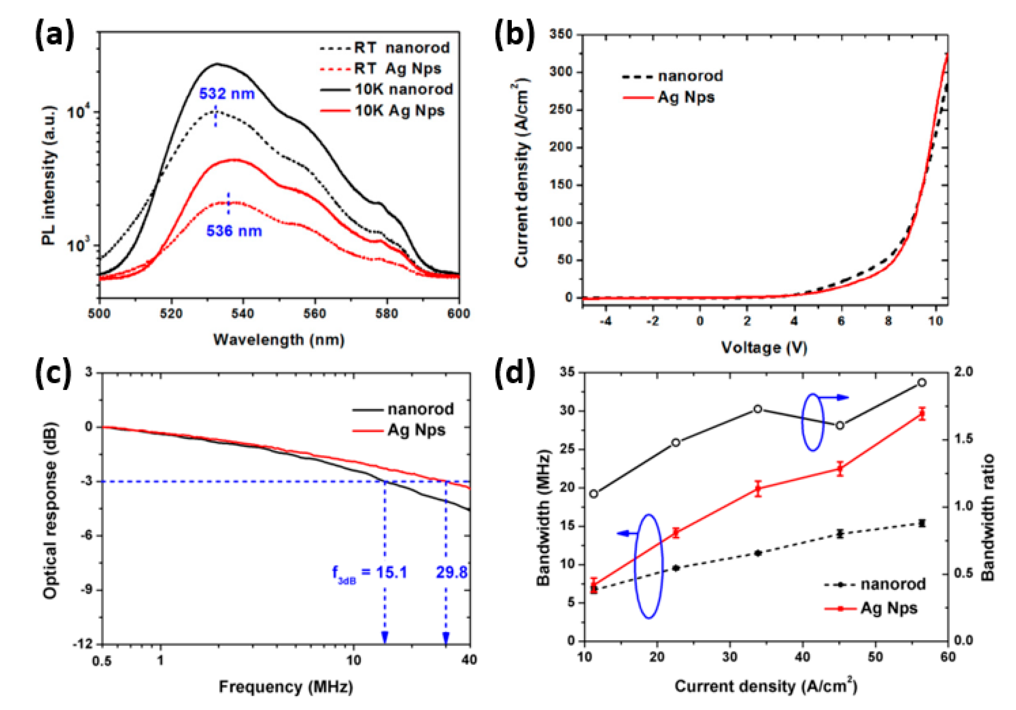
7. Improvement of Modulation Bandwidth

Even though various μ-LEDs for VLC applications exhibit high modulation bandwidths for short distances, some challenges still remain when implemented for long distance transmission. The modulation bandwidth for the commercial white LEDs based on Y3Al5O12:Ce3+ (YAG:Ce) phosphor is quite low due to the long carrier lifetime resulting in a limited transmission rate [90]. Hence, increasing the modulation bandwidth of the source of white light becomes a key issue. Researchers have therefore made significant efforts to design high-speed white emitting GaN-based LEDs and make further improvement in the existing bandwidth. To date, several approaches have been made to increase the modulation bandwidth in order to minimize the RC time constant by decreasing the active layer thickness, using the barrier dop-ed MQs, and by decreasing the effective active region. However, once the size of the LEDs exceeds its limit, the RC time cannot be further decreased and the bandwidth is constrained by the recombination time. Hence, several studies reported various ways of improving the modulation bandwidth, such as optimizing the LED chips structure, using blue-filter and using equalization circuit. Since high capacitance can be attributed to large chip size, it is important to optimize the structure of LED chips, as their layer structure specifies the bandwidth of a high-power LED. Optimization of LEDs can be achieved in various ways, which are intended to reduce the RC time constant and carrier recombination time, thus increasing the modulation bandwidth of LED chips. In addition, blue filter is another crucial component for VLC phosphor-based white LEDs that could effectively eliminate unwanted signals and increase the data rate, but it cannot influence the modulation bandwidth of the system. Some studies also indicated that an equalization circuit consisting of a resistor, inductor, and capacitor could reduce the signal distortions and increase the modulation bandwidth.
Yeh et al. demonstrated a phosphor-LED VLC and found that using pre-equalization technology, the modulation bandwidth of the phosphor-LED increases from 1 MHz to 12 MHz without utilizing the blue filter [91]. Figure 14a illustrates the pre-equalization Resistance-Inductance-Capacitance (RLC) circuit for compensation for LED impedance matching. The pre-equalization technique will certainly increase the modulation bandwidth by reducing signal distortion. However, the values of resistance and capacitance need to be adjusted to obtain the ideal pre-equalization characteristic. Moreover, the LED lighting must have a decent modulation bandwidth to accomplish a real-time VLC framework. Figure 14b–f display the modulation bandwidth for the phosphor-LED with and without the pre-equalization technique. It is clear that without pre-equalization, the bandwidth of the LED is 1.2 MHz, but when the pre-equalization technique is implemented, the measured bandwidth lies between 11.6 MHz and 12.1 MHz. Therefore, the modulation bandwidth of LEDs for VLC applications can be significantly increased using the pre-equalization technique.
Keeping in mind the various approaches stated above, Xiao et al., as part of the study to improve modulation bandwidth, showed that the modulation bandwidth could be improved by incorporating quantum dots (QDs) with LED [92]. Since QDs have the potential to confine the excitons resulting in a short fluorescent lifetime that is much less than commercial phosphorus, QD-LED could enhance not only the color quality but also the white LED bandwidth to achieve better performance for VLC [93]. To analyze the impact of QDs on modulation bandwidth, LEDs based on YAG:Ce phosphor, red QDs, green QDs and a mixture of red and green QD solutions have been developed. Figure 15a,b display the frequency response and modulation bandwidth comparisons for various LEDs, including fabricated ones and blue LED chips that do not contain phosphor or QDs. The measured 3dB bandwidth for the LEDs based on phosphor, red QDs, green QDs, red and green QDs mixture, and GaN LED chip are, respectively, 1.55 MHz, 2.70 MHz, 2.55 MHz, 2.60 MHz and 3.65 MHz. It is evident from the figure that there is an increase in the modulation bandwidth of 74.19% to phosphor-based LEDs with the implementation of red QDs, while the green QD-LED and QD-WLED show a reasonable bandwidth with improvements of 64.52% and 67.75%. However, of all these LEDs, the GaN LED chip has the best performance in terms of both frequency response and modulation bandwidth reaching up to 3.65 MHz.
In the research of Xiao et al., luminescent microspheres (LMS) were developed to enhance the optical efficiency of QDs and sustain large luminescent properties of QDs in white LED. LMS is fabricated by incorporating CdSe/ZnS QDs and the silica microsphere. LED-based LMS were designed to study the influence of fluorescent microspheres in the modulation bandwidth. Figure 16a,b display the LEDs based on YAG:Ce phosphor and the red LMS layer, respectively, along with their emission light. The phosphor-based LED exhibits a luminous efficacy of 119.23 lm/W corresponding to applied current of 54 mA and voltage of 2.84 V, while the LED based on LMS shows a luminous efficacy of 23.761 lm/W, corresponding to 1.98 V applied voltage and a current of 90 mA. Figure 16c,d display comparisons of frequency response and modulation bandwidth between phosphor-based LEDs and LMS, and it is found that the LED with LMS exhibits a higher 3dB bandwidth of 1.90 MHz than that of a 1.55 MHz phosphor-based LED. It can be realized that the bandwidth for LEDs can be improved by 22.58% using LMS as the light conversion material compared to phosphor. However, the LMS-based LED bandwidth is not as high as the QD solution-based bandwidth because there are some defects forming in the synthesis phase that result in lower light attenuation. Although having a lower bandwidth, LMS-based LEDs have long-term operating performance compared to QD-based solutions, and, thus, LMS still has great potential for QD-LED-based VLC.
As mentioned in the above section, the modulation bandwidth is limited by the size of the chips which will degrade the performance of the VLC application. Several research reports have been made based on the fact that because of QW- Surface Plasmon (SP) coupling, SPs can establish a new energy transition channel between electron and holes and thus increase the rate of the radiative recombination considerably [94,95]. SPs have higher state density that leads to a faster QW-SP coupling rate, thereby increasing the recombination rate and reducing the carrier lifetime. Hence, Shi-Chao Zhu et al. demonstrated Surface Plasmon (SP) coupled with GaN-based nanorod LEDs and Ag nanoparticles, showing that SPs would improve the modulation bandwidth [39]. Figure 17 demonstrates the schematic flow of GaN-LED fabrication based on nanorod and Ag nanoparticles (NPs). Metal organic chemical vapor deposition (MOCVD) is used to fabricate the GaN-based LED epilayers consisting of 18 pairs of InGaN/GaN MQWs created on the top of 3 µm thick Si-doped n-type GaN. The 35 nm thick Al2O3 layer is deposited on the top of p-type GaN, which was created above the MQWs, followed by the deposition of the 10nm thick Ni layer. After rapid thermal annealing (RTA), inductively coupled plasma (ICP) etching was conducted for the Al2O3, p-GaN and the active layer with a 25 nm etched depth in order to create a nanorod structure. Then, HfO2 is deposited to shield the nanorod and the active layer and is later coated by an Ag layer, which will become Ag nanoparticles after RTA under N2 at a temperature of 550 °C. After getting the Ag NPs on the top of the device, the space between the nanorods is filled with spin-on-glass (SOG) with a thickness of 500 nm, and this is baked in a furnace for 30 min at 550 °C, as shown in Figure 17d. Finally, ICP etching has been performed for the mesa to expose the n-type and p-type GaN layer for electrode deposition. After the metal electrode deposition using Cr/Pt/Au, the device is ready, as illustrated in Figure 17f. Another nanorod LED structure has also been created to check the influence of Ag NPs on the modulation bandwidth of the device.
In the following section, the electrical as well as optical characteristics of the two LEDs with and without Ag NPs were performed and analyzed. The photoluminescence (PL) spectra of the two LEDs have been recorded at two different conditions, as shown in Figure 18a, one at room temperature and another at 10 K, to evaluate the corresponding IQE of the two LEDs. The IQE of the nanorod LED with Ag NPs at room temperature is found to be 61%, which is higher than that without Ag NPs, i.e., 51%. The higher IQE of the LED with Ag NPs can be attributed to a strong QW-SP coupling, which leads to an efficient energy transfer from excitons in MQWs to SPs. Furthermore, there is a peak wavelength shift of about 4 nm, and the PL intensity of the LED with Ag NPs is reduced by 4.6 times that with Ag NPs. This reduction in PL intensity correlates to the MQWs region’s high IQE and the low scattering efficiency of Ag NPs, as most of the SP energy is dissipated rather than scattered due to the small Ag NP size. However, while the device’s luminous efficacy is very low, the QW-SP coupling can create a new energy transition channel for the electron–hole pairs, resulting in an improvement in the spontaneous emission rate for high-speed LED implementation. Moreover, because of its high quality factor and high Purcell factor, the small size Ag NPs can significantly increase the spontaneous emission rate [96,97]. Figure 18b shows the J–V characteristics of the nanorod LEDs with and without Ag NPs, showing a turn-on voltage of about 4V for both devices. Based on the J–V characteristics, the series resistances of nanorod LEDs with and without Ag NPs have been evaluated, and they were found to be 67 Ω and 89 Ω, respectively. The capacitances for both the LEDs with and without Ag NPs have been calculated, and they were found to be 3 pF corresponding to a current density of 57 A/cm2. Using these values of series resistances and capacitances, the calculated RC-limited bandwidths of the two LEDs with and without Ag NPs are about 790 MHz and 590 MHz, respectively. However, these calculated values of modulation bandwidths are much higher than the measured value, which is approximately 30 MHz for the LED with Ag NPs.
The measured 3-dB modulation bandwidth of the two devices with and without Ag NPs at an injection current density of 57 A/cm2 are 15.1 MHz and 29.8 MHz, respectively, as shown in Figure 18c. The lower modulation bandwidth is restricted by the carrier recombination lifetime. However, the modulation bandwidth for the LED with Ag NPs is found to be two times higher that without Ag NPs, suggesting that the spontaneous emission rate can be significantly improved by QW-SP coupling, thereby decreasing the carrier recombination lifetime. The modulation bandwidths of the two devices as a function of the injected current density are illustrated in Figure 18d, showing that the bandwidth increases with an increase in the injected current density. The modulation bandwidth ratio of the LED with Ag NPs to the LED without Ag NPs is shown in Figure 18d, and it is found to be increasing from 1.1 to 1.9 with increasing current density, which may be due to increasing IQE. The modulation bandwidth ratio is related to the IQE as M = ( F 1 ) η i n t + 1 , where M is the modulation bandwidth ratio, F is the Purcell factor, and η i n t is the IQE. Therefore, LEDs with higher IQE will have a higher modulation bandwidth by enhancing the radiative recombination rate. Since QW-SP coupling is found to increase the IQE for the corresponding LEDs, QW-SP coupling can effectively improve the modulation bandwidth.

8. Overview of VLC Emerging over the Last Few Years and Its Future Prospects

As discussed in the Introductory section of this paper, visible light communication is wireless communication technology in which visible light is used to modulate the baseband signal. Light-emitting diodes (LEDs) are preferred to realize VLC systems as they offer multiple exciting benefits over traditional light sources in terms of cost, efficiency, energy consumption and lifetime. VLC is thought to be a future technology that has the potential to be used in the indoor environment for data transmission with the advantages of minimum security threats. Extension of bandwidth and increasing data transmission rates are the two of the main challenges faced by the researchers working in the field of VLC.
The use of an efficient light source is an important consideration and an accomplishment of a VLC system. Phosphor-converted white LEDs are advantageous as they have less modulation complexity, but they perform poorly when it comes to the efficient utilization of the spectrum. We need to integrate LEDs of all three primary colors if spectrum utilization is to be maximized, but this results in modulation complexity and an increase in cost. If some low cost methods are developed that can help in the fabrication of full-color LEDs incorporating all three primary colors, we can realize a low-cost VLC system with efficient spectrum utilization. Besides white LEDs, dual- or multi-color emitting devices have also been used as VLC transmitters. Furthermore, instead of a single device, arrays of LEDs are also being utilized in VLC technology, which provides benefits in terms of higher output optical power. Solutions like this are also needed to be taken into account, and LED arrays with multi-color emission should also be investigated for VLC applications. Transmission distance is another concern associated with VLC technology. VLC systems realized until now lack the advantage of long-distance transmission and reception of data. Factors hindering long-distance transmission in VLC should be investigated thoroughly and addressed accordingly. Use of better quality light sources like lasers can also contribute somehow to the improvement of VLC systems. Researchers working in the field of VLC are continuously exploring the ways to maximize bandwidth and enhance transmission speeds of VLC systems. Separating slow-responding components of the light from transmitted signals can help in increasing the bandwidth, as reported by [98]. The use of an appropriate modulation scheme is also crucial, for example, OFDM can account effectively for degradation factors, multipath fading and inter-symbol interference, and, hence, high transmission speeds can be attained. Equalization is something that can also contribute to the improvement of bandwidths for VLC systems. Photodetectors are the commonly used tools for the purpose of detection in the field of VLC. Other kinds of detectors should also be explored, as photodetectors are usually very prone to the noise signal. At the moment, there is still no strong agreement about how and where VLC could effectively be used for future wireless communications technology. In addition, the transmission distance is constrained as the distance increases, leading to a significant decrease in optical power. To improve the transmission distance for an efficient device application, high-performance and low-cost transmitter and receiver modules or chips need to be designed, and equalizer optimization and hardware design for OFDM modulation schemes are essential. In new VLC technology, the primary attraction for research will be the real-time, low-cost and low-complexity framework. Therefore, it is the duty of all researchers working in this field to make every effort to contribute to VLC technology mechanization.

9. Conclusions

VLC technology has emerged as an alternative to RF communication because of the many advantages that VLC provides over RF. The above sections demonstrated the potential of the VLC system, which can achieve bandwidths of up to 1 GHz and transmission speeds of up to 2 Gbps. This review paper explains in brief the factors affecting the modulation bandwidth in LEDs, such as QCSE, carrier localization effect, carrier lifetime, etc. The potential use of semipolar μ-LEDs for the purposes of the VLC has been well established and proposed by many researchers. Since the optical power of a single μ-LED is very low due to its limited light-emitting area, it is preferable to make μ-LED arrays to increase optical power; thus, its use for VLC applications is very significant. The latest developments and advancements of device performance for VLC applications using semipolar μ-LEDs and μ-LED arrays have been elaborated in this study. Another important application of VLC, which is communications underwater, was also described in detail. In this paper, we have presented numerous approaches that can greatly improve the modulation bandwidth of the VLC system, but there are still some challenges that need to be addressed in the near future. Despite having these issues, VLC will remain an innovation, and a breakthrough is expected in the coming years.

Author Contributions

Data curation, A.-C.L., F.-J.L., and T.A.; project administration, C.-C.L., C.-W.C., and G.-R.L.; supervision, S.-W.H.C. and H.-C.K.; writing—original draft, K.J.S. and Y.-M.H.; writing—review and editing, T.W. All authors have read and agreed to the published version of the manuscript.

Funding

Ministry of Science and Technology, Taiwan (107-2221-E-009-113-MY3, 108-2221-E-009-113-MY3, 1092124-M-009-101); National Natural Science Foundation of China (11904302).

Acknowledgments

The authors would like to thank Zhong Chen of Xiamen University, Kei may Lau of HKUST and Jung Han of Yale University for helpful discussions.

Conflicts of Interest

The authors declare no conflict of interest.

References

  1. Karunatilaka, D.; Zafar, F.; Kalavally, V.; Parthiban, R. LED Based Indoor Visible Light Communications: State of the Art. IEEE Commun. Surv. Tutor. 2015, 17, 1649–1678. [Google Scholar] [CrossRef]
  2. Rehman, S.U.; Ullah, S.; Chong, P.H.; Yongchareon, S.; Komosny, D. Visible Light Communication: A System Perspective—Overview and Challenges. Sensors 2019, 19, 1153. [Google Scholar] [CrossRef] [Green Version]
  3. Hussain, B.; Li, X.; Che, F.; Patrick Yue, C.; Wu, L. Visible Light Communication System Design and Link Budget Analysis. J. Lightwave Technol. 2015, 33, 5201–5209. [Google Scholar] [CrossRef]
  4. Ismail, S.N.; Salih, M.H. A review of visible light communication (VLC) technology. AIP Conf. Proc. 2020, 2213, 020289. [Google Scholar]
  5. Kadirvelu, S.B.V. Design and implementation of visible light communication system in indoor environment. ARPN J. Eng. Appl. Sci. 2015, 10, 2882–2886. [Google Scholar]
  6. Khan, L.U. Visible light communication: Applications, architecture, standardization and research challenges. Digit. Commun. Netw. 2017, 3, 78–88. [Google Scholar] [CrossRef] [Green Version]
  7. Zhao, S.; Xu, J.; Trescases, O. A Dimmable LED Driver for Visible Light Communication (VLC) Based on LLC Resonant DC-DC Converter Operating in Burst Mode. In Proceedings of the Twenty-Eighth Annual IEEE Applied Power Electronics Conference and Exposition (APEC), Long Beach, CA, USA, 17–21 March 2013; pp. 2144–2150. [Google Scholar]
  8. Ji, R.; Wang, S.; Liu, Q.; Lu, W. High-Speed Visible Light Communications: Enabling Technologies and State of the Art. Appl. Sci. 2018, 8, 589. [Google Scholar] [CrossRef] [Green Version]
  9. Chow, C.W.; Yeh, C.H.; Liu, Y.F.; Liu, Y. Improved modulation speed of LED visible light communication system integrated to main electricity network. Electron. Lett. 2011, 47, 867–868. [Google Scholar] [CrossRef] [Green Version]
  10. Alavi, S.E.; Amiri, I.S.; Supa'at, A.S.M.; Idrus, S.M. Indoor Data Transmission Over Ubiquitous Infrastructure of Powerline Cables and LED Lighting. J. Comput. Theor. Nanosci. 2015, 12, 599–604. [Google Scholar] [CrossRef]
  11. Uema, H.; Matsumura, T.; Saito, S.; Murata, Y. Research and Development on Underwater Visible Light Communication Systems. Electron. Commun. Jpn. 2015, 98, 9–13. [Google Scholar] [CrossRef]
  12. Watson, S.; Viola, S.; Giuliano, G.; Najda, S.; Perlin, P.; Suski, T.; Marona, L.; Leszczyński, M.; Wisniewski, P.; Czernecki, R.; et al. High Speed Visible Light Communication Using Blue GaN Laser Diodes; SPIE: Edinburgh, UK, 2016; Volume 9991. [Google Scholar]
  13. Arnon, S. Optimised optical wireless car-to-traffic-light communication. Trans. Emerg. Telecommun. Technol. 2014, 25, 660–665. [Google Scholar] [CrossRef]
  14. Luo, P.; Tsai, H.-M.; Viriyasitavat, W.; Minh, H.; Tang, X. Car-to-Car Visible Light Communications: Theory and Applications; Taylor & Francis Group: Boca Raton, FL, USA, 2017; pp. 253–282. [Google Scholar]
  15. Farr, N.; Bowen, A.; Ware, J.; Pontbriand, C.; Tivey, M. An Integrated, Underwater Optical/Acoustic Communications System. In Proceedings of the OCEANS'10 IEEE SYDNEY, Sydney, Australia, 24–27 May 2010; pp. 1–6. [Google Scholar]
  16. Qureshi, U.M.; Shaikh, F.K.; Aziz, Z.; Shah, S.M.Z.S.; Sheikh, A.A.; Felemban, E.; Qaisar, S.B. RF Path and Absorption Loss Estimation for Underwater Wireless Sensor Networks in Different Water Environments. Sensors 2016, 16, 890. [Google Scholar] [CrossRef]
  17. Doniec, M.; Vasilescu, I.; Chitre, M.; Detweiler, C.; Hoffmann-Kuhnt, M.; Rus, D. Aquaoptical: A Lightweight Device for High-Rate Long-Range Underwater Point-To-Point Communication. In Proceedings of the OCEANS 2009, Biloxi, MS, USA, 26–29 October 2009; pp. 1–6. [Google Scholar]
  18. Hossan, M.T.; Chowdhury, M.; Hasan, M.K.; Shahjalal, M.; Nguyen, T.; Le, N.-T.; Jang, Y.M. A New Vehicle Localization Scheme Based on Combined Optical Camera Communication and Photogrammetry. Mob. Inf. Syst. 2018, 2018, 14. [Google Scholar] [CrossRef] [Green Version]
  19. Zhu, S.; Lin, S.; Li, J.; Yu, Z.; Cao, H.; Yang, C.; Li, J.; Zhao, L. Influence of quantum confined Stark effect and carrier localization effect on modulation bandwidth for GaN-based LEDs. Appl. Phys. Lett. 2017, 111, 171105. [Google Scholar] [CrossRef]
  20. Ryou, J.H.; Lee, W.; Limb, J.; Yoo, D.; Liu, J.P.; Dupuis, R.D.; Wu, Z.H.; Fischer, A.M.; Ponce, F.A. Control of quantum-confined Stark effect in InGaN∕GaN multiple quantum well active region by p-type layer for III-nitride-based visible light emitting diodes. Appl. Phys. Lett. 2008, 92, 101113. [Google Scholar] [CrossRef]
  21. Zhang, Y.; Smith, R.M.; Hou, Y.; Xu, B.; Gong, Y.; Bai, J.; Wang, T. Stokes shift in semi-polar (11–22) InGaN/GaN multiple quantum wells. Appl. Phys. Lett. 2016, 108, 031108. [Google Scholar] [CrossRef]
  22. Piprek, J. Efficiency droop in nitride-based light-emitting diodes. Phys. Status Solidi 2010, 207, 2217–2225. [Google Scholar] [CrossRef]
  23. Kozlowski, G.; Schulz, S.; Corbett, B. Polarization matching design of InGaN-based semi-polar quantum wells—A case study of (112¯2) orientation. Appl. Phys. Lett. 2014, 104, 051128. [Google Scholar] [CrossRef] [Green Version]
  24. Chen, S.-W.H.; Huang, Y.-M.; Singh, K.J.; Hsu, Y.-C.; Liou, F.-J.; Song, J.; Choi, J.; Lee, P.-T.; Lin, C.-C.; Chen, Z.; et al. Full-color micro-LED display with high color stability using semipolar (20-21) InGaN LEDs and quantum-dot photoresist. Photon. Res. 2020, 8, 630–636. [Google Scholar] [CrossRef]
  25. Rosales, D.; Gil, B.; Bretagnon, T.; Guizal, B.; Izyumskaya, N.; Monavarian, M.; Zhang, F.; Okur, S.; Avrutin, V.; Özgür, Ü.; et al. Recombination dynamics of excitons with low non-radiative component in semi-polar (10-11)-oriented GaN/AlGaN multiple quantum wells. J. Appl. Phys. 2014, 116, 093517. [Google Scholar] [CrossRef]
  26. Rosales, D.; Gil, B.; Bretagnon, T.; Guizal, B.; Zhang, F.; Okur, S.; Monavarian, M.; Izyumskaya, N.; Avrutin, V.; Özgür, Ü.; et al. Excitonic recombination dynamics in non-polar GaN/AlGaN quantum wells. J. Appl. Phys. 2014, 115, 073510. [Google Scholar] [CrossRef]
  27. Wu, T.; Sher, C.-W.; Lin, Y.; Lee, C.-F.; Liang, S.; Lu, Y.; Huang Chen, S.-W.; Guo, W.; Kuo, H.-C.; Chen, Z. Mini-LED and Micro-LED: Promising Candidates for the Next Generation Display Technology. Appl. Sci. 2018, 8, 1557. [Google Scholar] [CrossRef] [Green Version]
  28. Haemmer, M.; Roycroft, B.; Akhter, M.; Dinh, D.V.; Quan, Z.; Zhao, J.; Parbrook, P.J.; Corbett, B. Size-Dependent Bandwidth of Semipolar (11-22) Light-Emitting-Diodes. IEEE Photonics Technol. Lett. 2018, 30, 439–442. [Google Scholar] [CrossRef]
  29. Shi, J.; Sheu, J.; Chen, C.; Lin, G.; Lai, W. High-Speed GaN-Based Green Light-Emitting Diodes With Partially n-Doped Active Layers and Current-Confined Apertures. IEEE Electron Device Lett. 2008, 29, 158–160. [Google Scholar] [CrossRef]
  30. Liao, C.; Chang, Y.; Ho, C.; Wu, M. High-Speed GaN-Based Blue Light-Emitting Diodes With Gallium-Doped ZnO Current Spreading Layer. IEEE Electron Device Lett. 2013, 34, 611–613. [Google Scholar] [CrossRef]
  31. Liao, C.; Ho, C.; Chang, Y.; Wu, C.; Wu, M. High-Speed Light-Emitting Diodes Emitting at 500 nm With 463-MHz Modulation Bandwidth. IEEE Electron Device Lett. 2014, 35, 563–565. [Google Scholar] [CrossRef]
  32. McKendry, J.J.D.; Massoubre, D.; Zhang, S.; Rae, B.R.; Green, R.P.; Gu, E.; Henderson, R.K.; Kelly, A.E.; Dawson, M.D. Visible-Light Communications Using a CMOS-Controlled Micro-Light- Emitting-Diode Array. J. Lightwave Technol. 2012, 30, 61–67. [Google Scholar] [CrossRef] [Green Version]
  33. Wun, J.; Lin, C.; Chen, W.; Sheu, J.; Lin, C.; Li, Y.; Bowers, J.E.; Shi, J.; Vinogradov, J.; Kruglov, R.; et al. GaN-Based Miniaturized Cyan Light-Emitting Diodes on a Patterned Sapphire Substrate With Improved Fiber Coupling for Very High-Speed Plastic Optical Fiber Communication. IEEE Photonics J. 2012, 4, 1520–1529. [Google Scholar] [CrossRef]
  34. Windisch, R.; Knobloch, A.; Kuijk, M.; Rooman, C.; Dutta, B.; Kiesel, P.; Borghs, G.; Dohler, G.H.; Heremans, P. Large-signal-modulation of high-efficiency light-emitting diodes for optical communication. IEEE J. Quantum Electron. 2000, 36, 1445–1453. [Google Scholar] [CrossRef]
  35. Zhu, S.; Yu, Z.; Liu, L.; Yang, C.; Cao, H.; Xi, X.; Li, J.; Zhao, L. Enhancing the spontaneous emission rate by modulating carrier distribution in GaN-based surface plasmon light-emitting diodes. Opt. Express 2017, 25, 9617–9627. [Google Scholar] [CrossRef]
  36. Huang, S.-Y.; Horng, R.-H.; Shi, J.-W.; Kuo, H.-C.; Wuu, D.-S. High-Performance InGaN-Based Green Resonant-Cavity Light-Emitting Diodes for Plastic Optical Fiber Applications. J. Lightwave Technol. 2009, 27, 4084–4090. [Google Scholar] [CrossRef] [Green Version]
  37. Shi, J.; Chi, K.; Wun, J.; Bowers, J.E.; Shih, Y.; Sheu, J. III-Nitride-Based Cyan Light-Emitting Diodes With GHz Bandwidth for High-Speed Visible Light Communication. IEEE Electron Device Lett. 2016, 37, 894–897. [Google Scholar] [CrossRef]
  38. Maier, M.; Köhler, K.; Kunzer, M.; Pletschen, W.; Wagner, J. Reduced nonthermal rollover of wide-well GaInN light-emitting diodes. Appl. Phys. Lett. 2009, 94, 041103. [Google Scholar] [CrossRef]
  39. Zhu, S.-C.; Yu, Z.-G.; Zhao, L.-X.; Wang, J.-X.; Li, J.-M. Enhancement of the modulation bandwidth for GaN-based light-emitting diode by surface plasmons. Opt. Express 2015, 23, 13752–13760. [Google Scholar] [CrossRef]
  40. Huang, S.; Xian, Y.; Fan, B.; Zheng, Z.; Chen, Z.; Jia, W.; Jiang, H.; Wang, G. Contrary luminescence behaviors of InGaN/GaN light emitting diodes caused by carrier tunneling leakage. J. Appl. Phys. 2011, 110, 064511. [Google Scholar] [CrossRef]
  41. Li, Y.L.; Huang, Y.R.; Lai, Y.H. Efficiency droop behaviors of InGaN∕GaN multiple-quantum-well light-emitting diodes with varying quantum well thickness. Appl. Phys. Lett. 2007, 91, 181113. [Google Scholar] [CrossRef] [Green Version]
  42. Lefebvre, P.; Allègre, J.; Mathieu, H. Recombination dynamics of excitons in III-nitride layers and quantum wells. Mater. Sci. Eng. B 1999, 59, 307–314. [Google Scholar] [CrossRef]
  43. Malinauskas, T.; Miasojedovas, S.; Aleksiejūnas, R.; Juršėnas, S.; Jarašiūnas, K.; Nomura, M.; Arakawa, Y.; Shimura, T.; Kuroda, K. Direct study of nonlinear carrier recombination in InGaN quantum well structures. Phys. Status Solidi C 2011, 8, 2381–2383. [Google Scholar] [CrossRef]
  44. Mickevičius, J.; Tamulaitis, G.; Kuokštis, E.; Liu, K.; Shur, M.S.; Zhang, J.P.; Gaska, R. Well-width-dependent carrier lifetime in AlGaN∕AlGaN quantum wells. Appl. Phys. Lett. 2007, 90, 131907. [Google Scholar] [CrossRef]
  45. Cho, J.; Schubert, E.F.; Kim, J.K. Efficiency droop in light-emitting diodes: Challenges and countermeasures. Laser Photonics Rev. 2013, 7, 408–421. [Google Scholar] [CrossRef]
  46. Weisbuch, C.; Piccardo, M.; Martinelli, L.; Iveland, J.; Peretti, J.; Speck, J.S. The efficiency challenge of nitride light-emitting diodes for lighting. Phys. Status Solidi A 2015, 212, 899–913. [Google Scholar] [CrossRef]
  47. Okur, S.; Nami, M.; Rishinaramangalam, A.K.; Oh, S.H.; DenBaars, S.P.; Liu, S.; Brener, I.; Feezell, D.F. Internal quantum efficiency and carrier dynamics in semipolar (20-2-1) InGaN/GaN light-emitting diodes. Opt. Express 2017, 25, 2178–2186. [Google Scholar] [CrossRef]
  48. Rashidi, A.; Monavarian, M.; Aragon, A.; Okur, S.; Nami, M.; Rishinaramangalam, A.; Mishkat-Ul-Masabih, S.; Feezell, D. High-Speed Nonpolar InGaN/GaN LEDs for Visible-Light Communication. IEEE Photonics Technol. Lett. 2017, 29, 381–384. [Google Scholar] [CrossRef]
  49. Romanov, A.E.; Baker, T.J.; Nakamura, S.; Speck, J.S. Strain-induced polarization in wurtzite III-nitride semipolar layers. J. Appl. Phys. 2006, 100, 023522. [Google Scholar] [CrossRef] [Green Version]
  50. Monavarian, M.; Rashidi, A.; Aragon, A.; Oh, S.H.; Nami, M.; DenBaars, S.P.; Feezell, D. Explanation of low efficiency droop in semipolar (20-2-1) InGaN/GaN LEDs through evaluation of carrier recombination coefficients. Opt. Express 2017, 25, 19343–19353. [Google Scholar] [CrossRef]
  51. Monavarian, M.; Rashidi, A.; Aragon, A.A.; Oh, S.H.; Rishinaramangalam, A.K.; DenBaars, S.P.; Feezell, D. Impact of crystal orientation on the modulation bandwidth of InGaN/GaN light-emitting diodes. Appl. Phys. Lett. 2018, 112, 041104. [Google Scholar] [CrossRef]
  52. David, A.; Grundmann, M.J. Droop in InGaN light-emitting diodes: A differential carrier lifetime analysis. Appl. Phys. Lett. 2010, 96, 103504. [Google Scholar] [CrossRef]
  53. Yevick, D.; Streifer, W. Radiative and nonradiative recombination law in lightly doped InGaAsP lasers. Electron. Lett. 1983, 19, 1012–1014. [Google Scholar] [CrossRef]
  54. Feezell, D.F.; Speck, J.S.; DenBaars, S.P.; Nakamura, S. Semipolar (20-2-1) InGaN/GaN Light-Emitting Diodes for High-Efficiency Solid-State Lighting. J. Disp. Technol. 2013, 9, 190–198. [Google Scholar] [CrossRef]
  55. Rajpalke, M.K.; Roul, B.; Kumar, M.; Bhat, T.N.; Sinha, N.; Krupanidhi, S.B. Structural and optical properties of nonpolar (11−20) a-plane GaN grown on (1−102) r-plane sapphire substrate by plasma-assisted molecular beam epitaxy. Scr. Mater. 2011, 65, 33–36. [Google Scholar] [CrossRef]
  56. Mukundan, S.; Mohan, L.; Chandan, G.; Roul, B.; Krupanidhi, S.B. Semipolar and nonpolar GaN epi-films grown on m-sapphire by plasma assisted molecular beam epitaxy. J. Appl. Phys. 2014, 116, 204502. [Google Scholar] [CrossRef]
  57. Dinh, D.V.; Quan, Z.; Roycroft, B.; Parbrook, P.J.; Corbett, B. GHz bandwidth semipolar (11-22) InGaN/GaN light-emitting diodes. Opt. Lett. 2016, 41, 5752–5755. [Google Scholar] [CrossRef]
  58. Gong, Z.; Jin, S.; Chen, Y.; McKendry, J.; Massoubre, D.; Watson, I.M.; Gu, E.; Dawson, M.D. Size-dependent light output, spectral shift, and self-heating of 400 nm InGaN light-emitting diodes. J. Appl. Phys. 2010, 107, 013103. [Google Scholar] [CrossRef]
  59. Haggar, J.I.H.; Cai, Y.; Ghataora, S.S.; Smith, R.M.; Bai, J.; Wang, T. High Modulation Bandwidth of Semipolar (11–22) InGaN/GaN LEDs with Long Wavelength Emission. ACS Appl. Electron. Mater. 2020, 2, 2363–2368. [Google Scholar] [CrossRef]
  60. Chen, S.-W.H.; Huang, Y.-M.; Chang, Y.-H.; Lin, Y.; Liou, F.-J.; Hsu, Y.-C.; Song, J.; Choi, J.; Chow, C.-W.; Lin, C.-C.; et al. High-Bandwidth Green Semipolar (20–21) InGaN/GaN Micro Light-Emitting Diodes for Visible Light Communication. ACS Photonics 2020, 7, 2228–2235. [Google Scholar] [CrossRef]
  61. Hsu, C.-W.; Yeh, C.-H.; Chow, C.-W. Using adaptive equalization and polarization-multiplexing technology for gigabit-per-second phosphor-LED wireless visible light communication. Opt. Laser Technol. 2018, 104, 206–209. [Google Scholar] [CrossRef]
  62. Quan, Z.; Dinh, D.V.; Presa, S.; Roycroft, B.; Foley, A.; Akhter, M.; Mahony, D.O.; Maaskant, P.P.; Caliebe, M.; Scholz, F.; et al. High Bandwidth Freestanding Semipolar (11–22) InGaN/GaN Light-Emitting Diodes. IEEE Photonics J. 2016, 8, 1–8. [Google Scholar] [CrossRef] [Green Version]
  63. Shen, C.; Ng, T.K.; Leonard, J.T.; Pourhashemi, A.; Nakamura, S.; DenBaars, S.P.; Speck, J.S.; Alyamani, A.Y.; El-desouki, M.M.; Ooi, B.S. High-brightness semipolar (202-1) blue InGaN/GaN superluminescent diodes for droop-free solid-state lighting and visible-light communications. Opt. Lett. 2016, 41, 2608–2611. [Google Scholar] [CrossRef]
  64. Corbett, B.; Quan, Z.; Dinh, D.V.; Kozlowski, G.; O'Mahony, D.; Akhter, M.; Schulz, S.; Parbrook, P.; Maaskant, P.; Caliebe, M.; et al. Development of Semipolar (11-22) LEDs on GaN Templates; SPIE: San Francisco, CA, USA, 2016; Volume 9768. [Google Scholar]
  65. Khoury, M.; Li, H.; Li, P.; Chow, Y.C.; Bonef, B.; Zhang, H.; Wong, M.S.; Pinna, S.; Song, J.; Choi, J.; et al. Polarized monolithic white semipolar (20–21) InGaN light-emitting diodes grown on high quality (20–21) GaN/sapphire templates and its application to visible light communication. Nano Energy 2020, 67, 104236. [Google Scholar] [CrossRef]
  66. Li, X.; Wu, L.; Liu, Z.; Hussain, B.; Chong, W.C.; Lau, K.M.; Yue, C.P. Design and Characterization of Active Matrix LED Microdisplays With Embedded Visible Light Communication Transmitter. J. Lightwave Technol. 2016, 34, 3449–3457. [Google Scholar] [CrossRef]
  67. Rajbhandari, S.; McKendry, J.J.D.; Herrnsdorf, J.; Chun, H.; Faulkner, G.; Haas, H.; Watson, I.M.; O’Brien, D.; Dawson, M.D. A review of gallium nitride LEDs for multi-gigabit-per-second visible light data communications. Semicond. Sci. Technol. 2017, 32, 023001. [Google Scholar] [CrossRef]
  68. Choi, H.W.; Liu, C.; Gu, E.; McConnell, G.; Girkin, J.M.; Watson, I.M.; Dawson, M.D. GaN micro-light-emitting diode arrays with monolithically integrated sapphire microlenses. Appl. Phys. Lett. 2004, 84, 2253–2255. [Google Scholar] [CrossRef] [Green Version]
  69. Lin, H.-Y.; Sher, C.-W.; Hsieh, D.-H.; Chen, X.-Y.; Chen, H.-M.P.; Chen, T.-M.; Lau, K.-M.; Chen, C.-H.; Lin, C.-C.; Kuo, H.-C. Optical cross-talk reduction in a quantum-dot-based full-color micro-light-emitting-diode display by a lithographic-fabricated photoresist mold. Photon. Res. 2017, 5, 411–416. [Google Scholar] [CrossRef]
  70. Bui, H.Q.; Velpula, R.T.; Jain, B.; Aref, O.H.; Nguyen, H.-D.; Lenka, T.R.; Nguyen, H.P. Full-Color InGaN/AlGaN Nanowire Micro Light-Emitting Diodes Grown by Molecular Beam Epitaxy: A Promising Candidate for Next Generation Micro Displays. Micromachines 2019, 10, 492. [Google Scholar] [CrossRef] [Green Version]
  71. Xuan, T.; Shi, S.; Wang, L.; Kuo, H.-C.; Xie, R.-J. Inkjet-Printed Quantum Dot Color Conversion Films for High-Resolution and Full-Color Micro Light-Emitting Diode Displays. J. Phys. Chem. Lett. 2020, 11, 5184–5191. [Google Scholar] [CrossRef]
  72. Zhang, S.; Gong, Z.; McKendry, J.J.D.; Watson, S.; Cogman, A.; Xie, E.; Tian, P.; Gu, E.; Chen, Z.; Zhang, G.; et al. CMOS-Controlled Color-Tunable Smart Display. IEEE Photonics J. 2012, 4, 1639–1646. [Google Scholar] [CrossRef] [Green Version]
  73. Zhang, H.; Rogers, J.A. Recent Advances in Flexible Inorganic Light Emitting Diodes: From Materials Design to Integrated Optoelectronic Platforms. Adv. Opt. Mater. 2019, 7, 1800936. [Google Scholar] [CrossRef] [Green Version]
  74. Kim, H.-s.; Brueckner, E.; Song, J.; Li, Y.; Kim, S.; Lu, C.; Sulkin, J.; Choquette, K.; Huang, Y.; Nuzzo, R.G.; et al. Unusual strategies for using indium gallium nitride grown on silicon (111) for solid-state lighting. Natl. Acad. Sci. 2011, 108, 10072. [Google Scholar] [CrossRef] [Green Version]
  75. Ferreira, R.X.G.; Xie, E.; McKendry, J.J.D.; Rajbhandari, S.; Chun, H.; Faulkner, G.; Watson, S.; Kelly, A.E.; Gu, E.; Penty, R.V.; et al. High Bandwidth GaN-Based Micro-LEDs for Multi-Gb/s Visible Light Communications. IEEE Photonics Technol. Lett. 2016, 28, 2023–2026. [Google Scholar] [CrossRef] [Green Version]
  76. Islim, M.S.; Ferreira, R.X.; He, X.; Xie, E.; Videv, S.; Viola, S.; Watson, S.; Bamiedakis, N.; Penty, R.V.; White, I.H.; et al. Towards 10 Gb/s orthogonal frequency division multiplexing-based visible light communication using a GaN violet micro-LED. Photon. Res. 2017, 5, A35–A43. [Google Scholar] [CrossRef]
  77. Carreira, J.F.C.; Xie, E.; Bian, R.; Chen, C.; McKendry, J.J.D.; Guilhabert, B.; Haas, H.; Gu, E.; Dawson, M.D. On-chip GaN-based dual-color micro-LED arrays and their application in visible light communication. Opt. Express 2019, 27, A1517–A1528. [Google Scholar] [CrossRef] [PubMed]
  78. Ryou, J.; Yoder, P.D.; Liu, J.; Lochner, Z.; Kim, H.; Choi, S.; Kim, H.J.; Dupuis, R.D. Control of Quantum-Confined Stark Effect in InGaN-Based Quantum Wells. IEEE J. Sel. Top. Quantum Electron. 2009, 15, 1080–1091. [Google Scholar] [CrossRef]
  79. Xie, E.; He, X.; Islim, M.S.; Purwita, A.A.; McKendry, J.J.D.; Gu, E.; Haas, H.; Dawson, M.D. High-Speed Visible Light Communication Based on a III-Nitride Series-Biased Micro-LED Array. J. Lightwave Technol. 2019, 37, 1180–1186. [Google Scholar] [CrossRef] [Green Version]
  80. Tien, C.; Kuo, C.; Wuu, D.; Horng, R. Improved Optoelectronic Performance of High-Voltage Ultraviolet Light-Emitting Diodes Through Electrode Designs. IEEE Trans. Electron Devices 2017, 64, 4526–4531. [Google Scholar] [CrossRef]
  81. Huang, Y.; Guo, Z.; Huang, H.; Sun, H. Influence of Current Density and Capacitance on the Bandwidth of VLC LED. IEEE Photonics Technol. Lett. 2018, 30, 773–776. [Google Scholar] [CrossRef]
  82. Perin, J.K.; Sharif, M.; Kahn, J.M. Sensitivity Improvement in 100 Gb/s-per-Wavelength Links Using Semiconductor Optical Amplifiers or Avalanche Photodiodes. J. Lightwave Technol. 2016, 34, 5542–5553. [Google Scholar] [CrossRef]
  83. Liu, X.; Yi, S.; Zhou, X.; Zhang, S.; Fang, Z.; Qiu, Z.-J.; Hu, L.; Cong, C.; Zheng, L.; Liu, R.; et al. Laser-based white-light source for high-speed underwater wireless optical communication and high-efficiency underwater solid-state lighting. Opt. Express 2018, 26, 19259–19274. [Google Scholar] [CrossRef]
  84. Xu, J.; Kong, M.; Lin, A.; Song, Y.; Yu, X.; Qu, F.; Han, J.; Deng, N. OFDM-based broadband underwater wireless optical communication system using a compact blue LED. Opt. Commun. 2016, 369, 100–105. [Google Scholar] [CrossRef]
  85. Zeng, Z.; Fu, S.; Zhang, H.; Dong, Y.; Cheng, J. A Survey of Underwater Optical Wireless Communications. IEEE Commun. Surv. Tutor. 2017, 19, 204–238. [Google Scholar] [CrossRef]
  86. Fan, Z.Y.; Lin, J.Y.; Jiang, H.X. III-nitride micro-emitter arrays: Development and applications. J. Phys. D Appl. Phys. 2008, 41, 094001. [Google Scholar] [CrossRef]
  87. Schubert, E.F. Light-Emitting Diodes, 2nd ed.; Cambridge University Press: Cambridge, UK, 2006. [Google Scholar]
  88. Wei, Z.; Zhang, L.; Wang, L.; Chen, C.-J.; Pepe, A.; Liu, X.; Chen, K.-C.; Wu, M.-C.; Dong, Y.; Wang, L.; et al. 2  Gbps/3  m air–underwater optical wireless communication based on a single-layer quantum dot blue micro-LED. Opt. Lett. 2020, 45, 2616–2619. [Google Scholar] [CrossRef]
  89. Tian, P.; Liu, X.; Yi, S.; Huang, Y.; Zhang, S.; Zhou, X.; Hu, L.; Zheng, L.; Liu, R. High-speed underwater optical wireless communication using a blue GaN-based micro-LED. Opt. Express 2017, 25, 1193–1201. [Google Scholar] [CrossRef]
  90. Wang, Y.; Wang, Y.; Chi, N.; Yu, J.; Shang, H. Demonstration of 575-Mb/s downlink and 225-Mb/s uplink bi-directional SCM-WDM visible light communication using RGB LED and phosphor-based LED. Opt. Express 2013, 21, 1203–1208. [Google Scholar] [CrossRef]
  91. Yeh, C.-H.; Liu, Y.-L.; Chow, C.-W. Real-time white-light phosphor-LED visible light communication (VLC) with compact size. Opt. Express 2013, 21, 26192–26197. [Google Scholar] [CrossRef]
  92. Xiao, X.; Tang, H.; Zhang, T.; Chen, W.; Chen, W.; Wu, D.; Wang, R.; Wang, K. Improving the modulation bandwidth of LED by CdSe/ZnS quantum dots for visible light communication. Opt. Express 2016, 24, 21577–21586. [Google Scholar] [CrossRef]
  93. Laurand, N.; Guilhabert, B.; McKendry, J.; Kelly, A.E.; Rae, B.; Massoubre, D.; Gong, Z.; Gu, E.; Henderson, R.; Dawson, M.D. Colloidal quantum dot nanocomposites for visible wavelength conversion of modulated optical signals. Opt. Mater. Express 2012, 2, 250–260. [Google Scholar] [CrossRef]
  94. Okamoto, K.; Niki, I.; Scherer, A.; Narukawa, Y.; Mukai, T.; Kawakami, Y. Surface plasmon enhanced spontaneous emission rate of InGaN∕GaN quantum wells probed by time-resolved photoluminescence spectroscopy. Appl. Phys. Lett. 2005, 87, 071102. [Google Scholar] [CrossRef] [Green Version]
  95. Okamoto, K.; Niki, I.; Shvartser, A.; Narukawa, Y.; Mukai, T.; Scherer, A. Surface-plasmon-enhanced light emitters based on InGaN quantum wells. Nat. Mater. 2004, 3, 601–605. [Google Scholar] [CrossRef]
  96. Purcell, E.M. Spontaneous Emission Probabilities at Radio Frequencies. In Confined Electrons and Photons: New Physics and Applications; Burstein, E., Weisbuch, C., Eds.; Springer US: Boston, MA, USA, 1995; p. 839. [Google Scholar]
  97. Sun, G.; Khurgin, J.B.; Soref, R.A. Practical enhancement of photoluminescence by metal nanoparticles. Appl. Phys. Lett. 2009, 94, 101103. [Google Scholar] [CrossRef] [Green Version]
  98. Langer, K.; Vucic, J.; Kottke, C.; Rosal, L.F.d.; Nerreter, S.; Walewski, J. Advances and Prospects in High-Speed Information Broadcast Using Phosphorescent White-Light LEDs. In Proceedings of the 2009 11th International Conference on Transparent Optical Networks, Azores, Portugal, 28 June–2 July 2009; pp. 1–6. [Google Scholar]
Figure 1. (a) Time-resolved photoluminescence spectra (TRPL) for light-emitting diodes (LEDs) with different quantum well (QW) thickness; (b) external quantum efficiency (EQE) for LEDs with different QW widths; (c) 3-dB modulation bandwidths. [19] Figures reproduced with permission from American Institute of Physics Publishing.
Applsci 10 07384 g001
Figure 2. (a) Modulation bandwidth and (b) differential carrier lifetime as a function of current density and (c) calculated log (n) vs. log (J) for LEDs with polar (green squares), semipolar (blue circles), and nonpolar (black triangles) orientations. [51] Figures reproduced with permission from American Institute of Physics Publishing.
Applsci 10 07384 g002
Figure 3. (a) Popt and corresponding EQE of the LED plotted as a function of I(J)inject; (b) normalized frequency response curves of the non-mesa-etched 50 μm diameter, 200 × 200 μm2, and 300 × 300 μm2 (11-22) LEDs measured at different Jinject (Iinject = 4 mA); (c) eye diagrams at 2 Gbps and 2.4 Gbps of an LED with a non-mesa-etched 50 μm diameter (11-22) measured at Iinject = 10 mA. [57] Figures reproduced with permission from Optical Society of America.
Applsci 10 07384 g003
Figure 4. (a) Schematic diagram of (20-21) µ-LED structures; (b) electroluminescence (EL) spectra at different currents and an image of lighting from the device; (c) Current density-Voltage (J–V) curve of the semipolar µ-LEDs. [60] Figures reproduced with permission from ACS Publications.
Applsci 10 07384 g004
Figure 5. (a) EL spectra at 50 mA along the x`- and y`-direction and the polarization ratio at different currents; (b) TRPL curve of semipolar and c-plane µ-LEDs. [60] Figures reproduced with permission from ACS Publications.
Applsci 10 07384 g005
Figure 6. (a) Frequency response measurement; (b) eye diagram for the data rate measurement. [60] Figures reproduced with permission from ACS Publications.
Applsci 10 07384 g006
Figure 7. (a) -6 dB modulation bandwidth for violet, green and blue µ-LEDs as a function of current density; (b) bit error rate (BER) versus data rate for blue and green µ-LEDs in both wavelength division multiplexing (WDM) schemes; (c) BER versus data rate for blue and violet µ-LEDs in both WDM schemes. [77] Figures reproduced with permission from Optical Society of America.
Applsci 10 07384 g007
Figure 8. For the blue-green µ-LED array: signal-to-noise ratio and allocated bits plots in both WDM schemes attained by (a) the blue µ-LED and (b) the green µ-LED; for the blue-violet µ-LED array: signal-to-noise ratio and allocated bits plots in both WDM schemes attained by (c) the blue µ-LED and (d) the violet µ-LED. [77] Figures reproduced with permission from Optical Society of America.
Applsci 10 07384 g008
Figure 9. (a) 6-dB electrical bandwidth of the series-biased µ-LED array; eye diagrams of (b) transmitted and (c) received signals using on-off keying (OOK) at a bit rate of 700 Mbps without an equalizer using the reported μ-LED array. [79] Figures reproduced with permission from IEEE.
Applsci 10 07384 g009
Figure 10. (a) Signal-to-noise (SNR) curve plotted against the bandwidth attained for Orthogonal Frequency-Division Multiplexing (OFDM) using the reported μ-LED array; (b) BER plotted against the data rate attained by adopting OOK, 4-PAM and OFDM modulation schemes. [79] Figures reproduced with permission from IEEE.
Applsci 10 07384 g010
Figure 11. Overview of underwater optical wireless communication.
Applsci 10 07384 g011
Figure 12. (a) Frequency response of the micro-LED at different injected currents; (b) -3dB modulation bandwidth as a function of current; (c) BER vs. data rate; (d) BER vs. received light output power. [89] Figures reproduced with permission from Optical Society of America.
Applsci 10 07384 g012
Figure 13. Eye diagrams at data rates of (a) 400 Mb/s and (b) 700 Mb/s using a p-i-n (PIN) photodetector; eye diagrams with received powers of (c) 80 µW and (d) 0.1 µW at 100 Mb/s using the Avalanche Photodiode (APD) photodetector. [89] Figures reproduced with permission from Optical Society of America.
Applsci 10 07384 g013
Figure 14. (a) Resistance-Inductance-Capacitance (RLC) circuit design for pre-equalization technology; (b) bandwidth of phosphor-LED without pre-equalization. The 3dB bandwidth of phosphor-LED with pre-equalization under received power of (c) 1100; (d) 900; (e) 700; (f) 500 Lux, respectively. [91] Figures reproduced with permission from Optical Society of America.
Applsci 10 07384 g014
Figure 15. Comparisons of (a) frequency responses and (b) modulation bandwidths for different LEDs with phosphor, red, green, a mixture QDs and without phosphor or QDs. [92] Figures reproduced with permission from Optical Society of America.
Applsci 10 07384 g015
Figure 16. (a) YAG:Ce phosphor-based LED; (b) LED with a red luminescent microspheres (LMS) layer; (c) frequency response comparison; (d) modulation bandwidth comparison between LEDs with phosphor and LMS. [92] Figures reproduced with permission from Optical Society of America.
Applsci 10 07384 g016
Figure 17. Schematic flow of GaN-based nanorod LED fabrication with Ag nanoparticles. [39] Figures reproduced with permission from Optical Society of America.
Applsci 10 07384 g017
Figure 18. (a) Photoluminescence (PL) spectra of nanorod LEDs with and without Ag NPs at room temperature and 10 K; (b) J–V characteristics of the nanorod LEDs with and without Ag NPs; (c) frequency response of the nanorod LED with and without Ag NPs; (d) modulation bandwidth of the two LEDs as a function of the injection current density. [39] Figures reproduced with permission from Optical Society of America.
Applsci 10 07384 g018
Table 1. Summary of the reported device performance of the semipolar LED-based Visible Light Communication (VLC) system.
Research Team LED typeDrive CurrentBandwidthData Rate
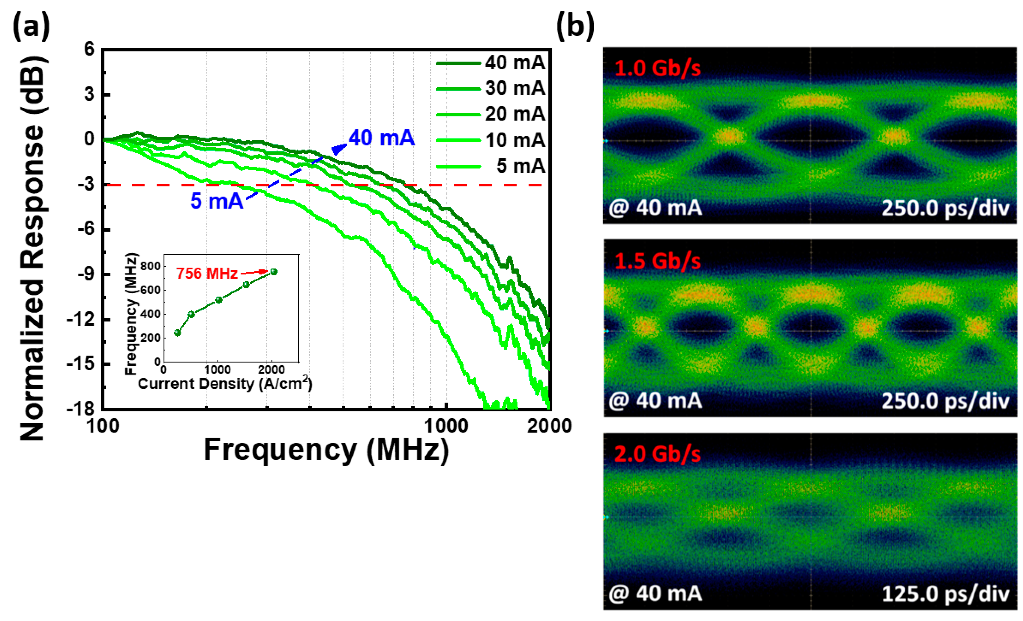
Dinh et al. [57]

Huang Chen et al. [60]
Hagger et al. [59]

Quan et al. [62]

Chao Shen et al. [63]
Corbett et al. [64]

Khoury et al. [65]
(11-22) InGaN/GaN blue LED
(20-21) InGaN/GaN green LED
(11-22) InGaN/GaN green
LED
(11-22) InGaN/GaN blue
LED
(20-2-1) InGaN/GaN super luminescent diode
(11-22) green LED on GaN template
(20-21) white InGaN LED on GaN/Sapphire template
4 mA

40 mA

92 A/cm2

20 mA

600 mA

30 mA

2 kA/cm2
1030 MHz

756 MHz

540 MHz

150 MHz

560 MHz

100 MHz

660 MHz
2.4 Gbps

1.5 Gbps

---

300 Mbps

---

---

---
Publisher’s Note: MDPI stays neutral with regard to jurisdictional claims in published maps and institutional affiliations.

