Sub-Picosecond Micromachining of Monocrystalline Silicon for Solar Cell Manufacturing


Abstract
1. Introduction
2. Experimental Setup
3. Results
4. Conclusions
Author Contributions
Funding
Conflicts of Interest
Data Availability
References
- Franta, B.; Mazur, E.; Sundaram, S.K. Ultrafast laser processing of silicon for photovoltaics. Int. Mater. Rev. 2017, 63, 227–240. [Google Scholar] [CrossRef]
- Carlson, D.E. Laser processing of solar cells. SPIE Solar Energy Technol. 2012, 8473, 847302. [Google Scholar] [CrossRef]
- Booth, H. Laser Processing in Industrial Solar Module Manufacturing. J. Laser Micro/Nanoeng. 2010, 5, 183–191. [Google Scholar] [CrossRef]
- Crouch, C.H.; Carey, J.E.; Warrender, J.M.; Aziz, M.J.; Mazur, E.; Génin, F.Y. Comparison of structure and properties of femtosecond and nanosecond laser-structured silicon. Appl. Phys. Lett. 2004, 84, 1850–1852. [Google Scholar] [CrossRef]
- Shen, M.Y.; Crouch, C.H.; Carey, J.E.; Mazur, E. Femtosecond laser-induced formation of submicrometer spikes on silicon in water. Appl. Phys. Lett. 2004, 85, 5694–5696. [Google Scholar] [CrossRef]
- Carey, J.E.; Crouch, C.H.; Shen, M.; Mazur, E. Visible and near-infrared responsivity of femtosecond-laser microstructured silicon photodiodes. Opt. Lett. 2005, 30, 1773–1775. [Google Scholar] [CrossRef]
- Huang, Z.; Carey, J.E.; Liu, M.; Guo, X.; Mazur, E.; Campbell, J.C. Microstructured silicon photodetector. Appl. Phys. Lett. 2006, 89, 033506. [Google Scholar] [CrossRef]
- Younkin, R.; Carey, J.E.; Mazur, E.; Levinson, J.A.; Friend, C.M. Infrared absorption by conical silicon microstructures made in a variety of background gases using femtosecond-laser pulses. J. Appl. Phys. 2003, 93, 2626. [Google Scholar] [CrossRef]
- Tull, B.R.; Carey, J.E.; Mazur, E.; McDonald, J.P.; Yalisove, S.M. Silicon Surface Morphologies after Femtosecond Laser Irradiation. MRS Bull. 2006, 31, 626–633. [Google Scholar] [CrossRef]
- Zhong, S.-L.; Wang, A. Rear emitter n-type passivated emitter, rear totally diffused silicon solar cell Structure. Appl. Phys. Lett. 2006, 88, 242102. [Google Scholar] [CrossRef]
- Sarnet, T.; Halbwax, M.; Torres, R.; Delaporte, P.; Sentis, M.; Martinuzzi, S.; Vervisch, V.; Torregrosa, F.; Etienne, H.; Roux, L.; et al. Femtosecond laser for black silicon and photovoltaic cells. Commer. Biomed. Appl. Ultrafast Lasers VIII 2008, 6881, 688119. [Google Scholar] [CrossRef]
- Dunsky, C. Laser Processes in PV Manufacturing: An Update. Industrial Laser Soultions for Manufacturing. 2011. Available online: http://www.industrial-lasers.com (accessed on 5 September 2020).
- Available online: https://www.directindustry.com/ (accessed on 8 October 2020).
- Bovatsek, J.M.; Patel, R.S. Highest-speed dicing of thin silicon wafers with nanosecond-pulse 355nm q-switched laser source using line-focus fluence optimization technique. In Proceedings of the SPIE LASE, San Francisco, CA, USA, 26–28 January 2010; p. 75850K. [Google Scholar]
- Neuenschwander, B.; Bucher, G.F.; Hennig, G.; Nussbaum, C.; Joss, B.; Muralt, M.; Zehnder, S.; Hunziker, U.W.; Schütz, P. Processing of dielectric materials and metals with PS laserpulses. In Proceedings of the International Congress on Applications of Lasers & Electro-Optics, Anaheim, CA, USA, 26–30 September 2010; p. 707. [Google Scholar]
- Liu, X.; Du, D.; Mourou, G. Laser ablation and micromachining with ultrashort laser pulses. IEEE J. Quantum Electron. 1997, 33, 1706–1716. [Google Scholar] [CrossRef]
- Rethfeld, B.; Sokolowski-Tinten, K.; Von Der Linde, D.; Anisimov, S. Timescales in the response of materials to femtosecond laser excitation. Appl. Phys. A 2004, 79, 767–769. [Google Scholar] [CrossRef]
- Kramer, T.; Remund, S.; Jäggi, B.; Schmid, M.; Neuenschwander, B. Ablation dynamics–from absorption to heat accumulation/ultra-fast laser matter interaction. Adv. Opt. Technol. 2018, 7, 129. [Google Scholar] [CrossRef]
- Garasz, K.; Kocik, M.; Petrov, T. Experimental investigations on ultrashort laser ablation for micro and nanomachining of materials. J. Physics Conf. Ser. 2019, 1186, 012028. [Google Scholar] [CrossRef]
- Photovoltaics Report. Fraunhofer Institute for Solar Energy Systems; FHG-SK: ISE-PUBLIC: Freiburg, Germany, 2019. [Google Scholar]
- Santbergen, R.; Van Zolingen, R. The absorption factor of crystalline silicon PV cells: A numerical and experimental study. Sol. Energy Mater. Sol. Cells 2008, 92, 432–444. [Google Scholar] [CrossRef]
- Shaheen, M.; Gagnon, J.E.; Fryer, B.J. Femtosecond laser ablation behavior of gold, crystalline silicon, and fused silica: A comparative study. Laser Phys. 2014, 24, 106102. [Google Scholar] [CrossRef]
- Boniecki, M.; Kamiński, P.; Wesołowski, W.; Krzyżak, K. Mechanical strength and fracture toughness of brittle monocrystalline and ceramic materials. Electron. Mater. 2016, 44, 8–16. [Google Scholar]
- Zeng, X.; Mao, X.; Greif, R.; Russo, R. Ultraviolet femtosecond and nanosecond laser ablation of silicon: Ablation efficiency and laser-induced plasma expansion. In Proceedings of the SPIE, Taos, NM, USA, 20 September 2004; Volume 5448, pp. 1150–1158. [Google Scholar]
- Lim, G.; Tuan, A.; Low, D.; Chen, Q. High quality laser microcutting of difficult-to-cut materials–copperand silicon wafer. In Proceedings of the ICALEO, Scottsdale, AZ, USA, 14–17 October 2002; p. 806103. [Google Scholar]
- Corboline, T.; Hoult, A.P. Laser machining of silicon using diode-pumped solid state & CO2 lasers. In Proceedings of the the ICALEO, Scottsdale, AZ, USA, 14–17 October 2002; p. 584220. [Google Scholar]
- Bonse, J.; Baudach, S.; Krüger, J.; Kautek, W.; Lenzner, M. Femtosecond laser ablation of silicon –modificationthresholds and morphology. Appied Phys. A 2002, 74, 19–25. [Google Scholar] [CrossRef]
- Rethfeld, B.; Ivanov, D.S.; Garcia, M.E.; Anisimov, S.I. Modelling ultrafast laser ablation. J. Phys. D Appl. Phys. 2017, 50, 193001. [Google Scholar] [CrossRef]
- Rämer, A.; Osmani, O.; Rethfeld, B. Laser damage in silicon: Energy absorption, relaxation, and transport. J. Appl. Phys. 2014, 116, 053508. [Google Scholar] [CrossRef]
- Clark, D. Lasers in solar cell production. Photonics Spectra 2009. Available online: https://www.photonics.com/Articles/Lasers_in_solar_cell_production/a40098 (accessed on 5 September 2020).


| TRUMPF TruMicro 5000 Series | COHERENT Monaco | IPG PHOTONICS GLPF Series | SPECTRA PHYSICS Spirit Series | |
|---|---|---|---|---|
| Operational mode | picosecond, short-pulse, femtosecond | femtosecond | short-pulse | femtosecond |
| Technology | solid-state | solid-state | fiber | solid-state |
| Spectrum | infrared | infrared, green | green | tunable, adjustable wavelength |
| Applications | industrial, for materials processing | industrial, cutting, for materials processing, drilling, pumping, for marking | cutting, drilling, for medical equipment, marking | industrial |
| Wavelength | 1030 nm | 517 nm, 1035 nm | 515 nm | 515 nm, 1,030 nm, 1040 nm |
| Power | Min.: 10 W Max.: 100 W | 20 W, 40 W | 5 W, 10 W, 20 W | Min.: 8 W, Max.: 100 W |
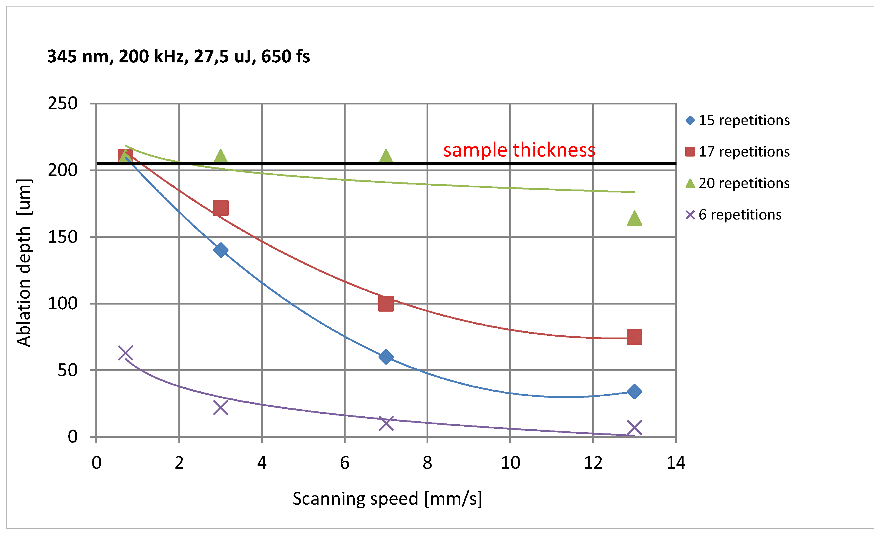
| V [mm/s] | Pattern Repetitions | P [W] | E [µJ] | Wavelength [nm] | Crater Width [µm] | Crater Depth [µm] |
|---|---|---|---|---|---|---|
| 7 mm/s | 15 | 5.5 | 27.5 | 343 | 55 | 60 |
| 7 mm/s | 17 | 5.5 | 27.5 | 343 | 75 | 100 |
| 7 mm/s | 20 | 5.5 | 27.5 | 343 | Cut trough | 210 |
Publisher’s Note: MDPI stays neutral with regard to jurisdictional claims in published maps and institutional affiliations. |
© 2020 by the authors. Licensee MDPI, Basel, Switzerland. This article is an open access article distributed under the terms and conditions of the Creative Commons Attribution (CC BY) license (http://creativecommons.org/licenses/by/4.0/).
Share and Cite
Garasz, K.; Kocik, M. Sub-Picosecond Micromachining of Monocrystalline Silicon for Solar Cell Manufacturing. Appl. Sci. 2020, 10, 7277. https://doi.org/10.3390/app10207277
Garasz K, Kocik M. Sub-Picosecond Micromachining of Monocrystalline Silicon for Solar Cell Manufacturing. Applied Sciences. 2020; 10(20):7277. https://doi.org/10.3390/app10207277
Chicago/Turabian StyleGarasz, Katarzyna, and Marek Kocik. 2020. "Sub-Picosecond Micromachining of Monocrystalline Silicon for Solar Cell Manufacturing" Applied Sciences 10, no. 20: 7277. https://doi.org/10.3390/app10207277
APA StyleGarasz, K., & Kocik, M. (2020). Sub-Picosecond Micromachining of Monocrystalline Silicon for Solar Cell Manufacturing. Applied Sciences, 10(20), 7277. https://doi.org/10.3390/app10207277