Mid-Infrared Grayscale Metasurface Holograms

 , and
, and 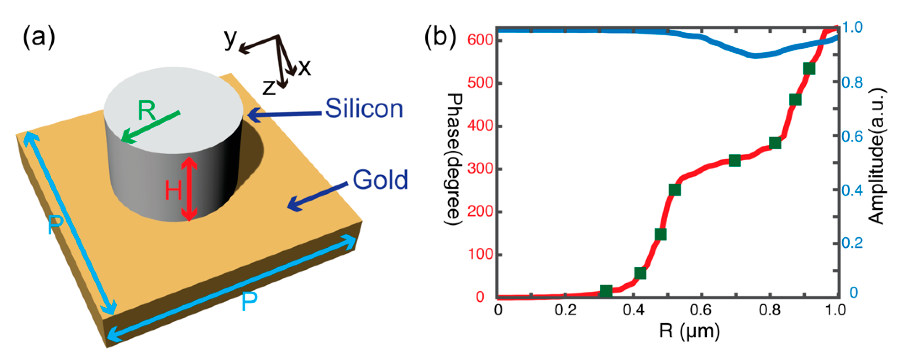
Abstract
1. Introduction
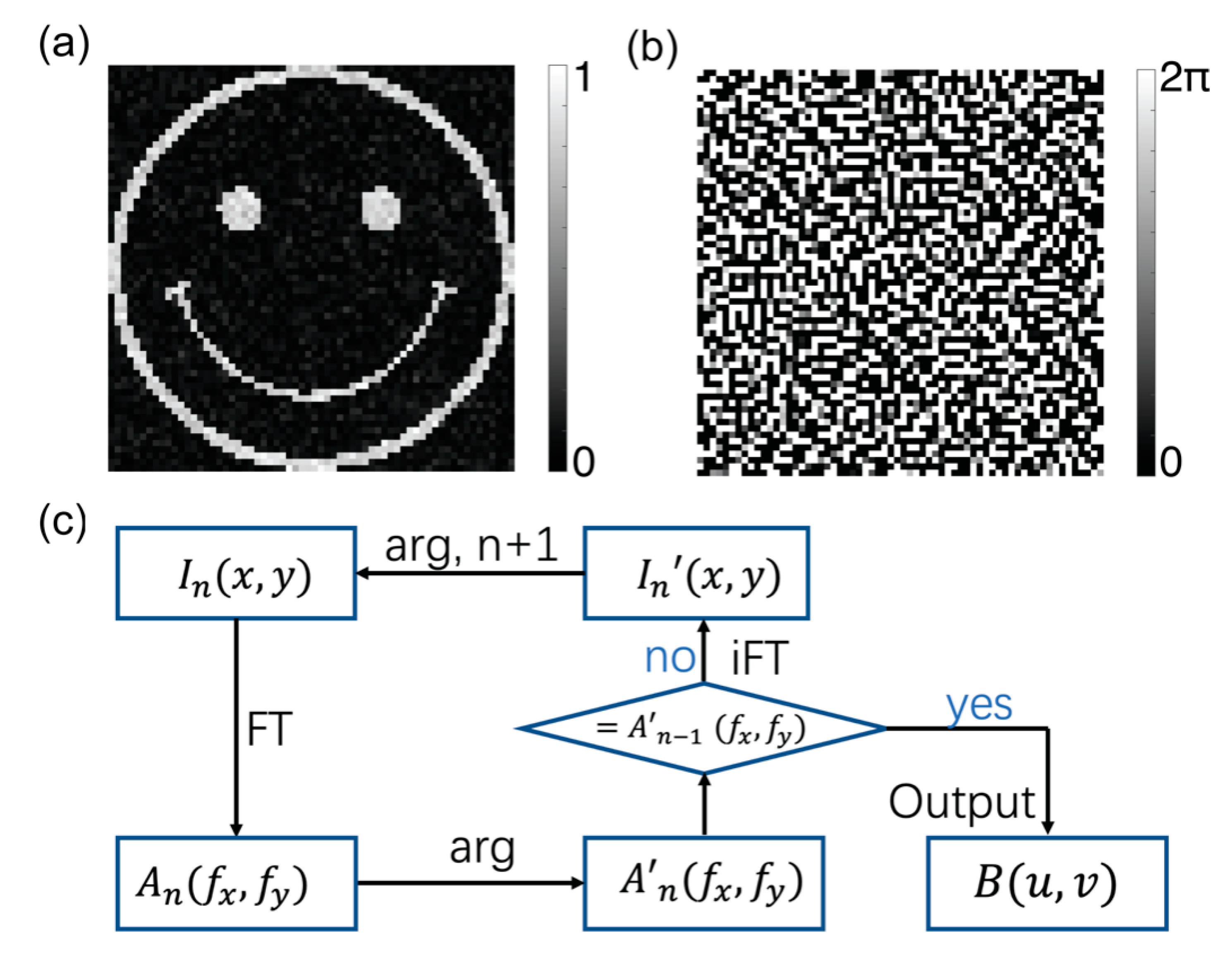
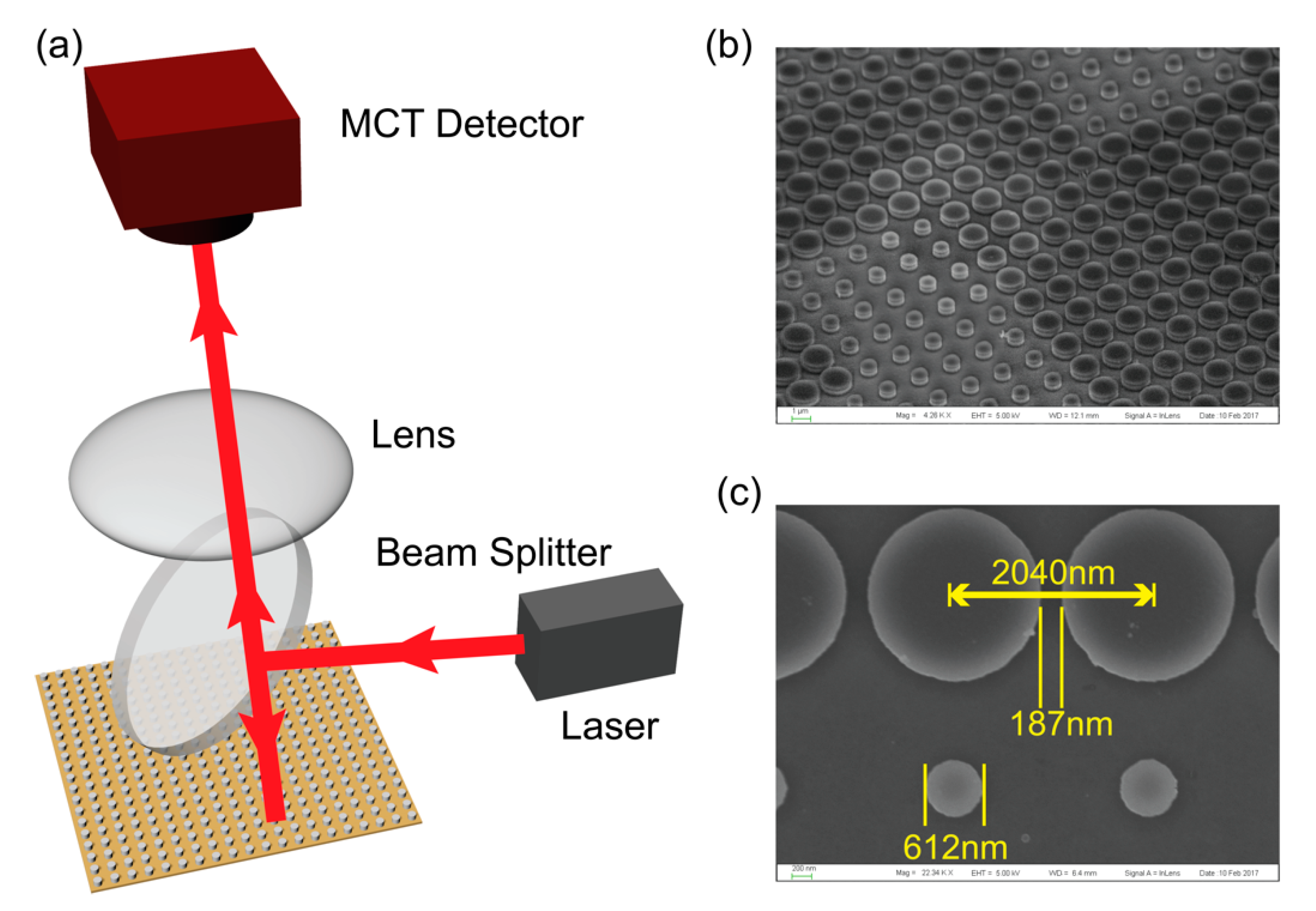
2. Materials and Methods
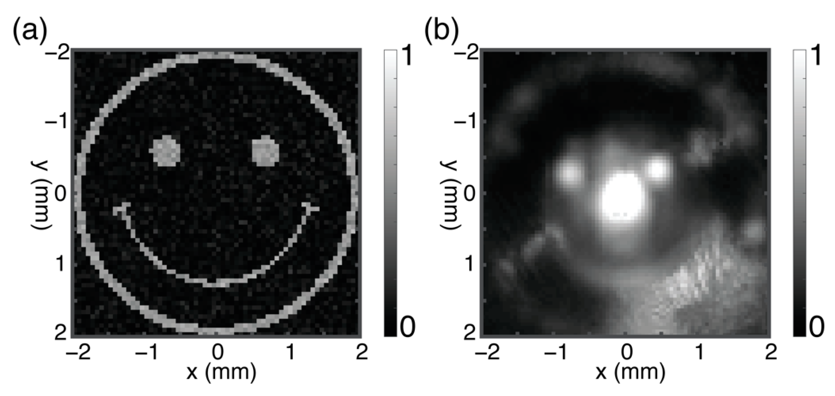
3. Results
4. Conclusions
Author Contributions
Funding
Acknowledgments
Conflicts of Interest
References
- Yu, N.; Genevet, P.; Kats, M.A.; Aieta, F.; Tetienne, J.-P.; Capasso, F.; Gaburro, Z. Light propagation with phase discontinuities: Generalized laws of reflection and refraction. Science 2011, 334, 333. [Google Scholar] [CrossRef] [PubMed]
- Neshevand, D.; Aharonovich, I. Optical metasurfaces: New generation building blocks for multi-functional optics. Light Sci. Appl. 2018, 7, 58. [Google Scholar] [CrossRef]
- Genevet, P.; Capasso, F.; Aieta, F.; Khorasaninejad, M.; Devlin, R. Recent advances in planar optics: From plasmonic to dielectric metasurfaces. Optica 2017, 4, 139. [Google Scholar] [CrossRef]
- Parsons, J.; Hendry, E.; Burrows, C.P.; Auguie, B.; Sambles, J.R.; Barnes, W.L. Localized surface-plasmon resonances in periodic nondiffracting metallic nanoparticle and nanohole arrays. Phys. Rev. B 2009, 79, 073412. [Google Scholar] [CrossRef]
- de Abajo, F.J.G. Colloquium: Light scattering by particle and hole arrays. Rev. Mod. Phys. 2007, 79, 1267. [Google Scholar] [CrossRef]
- Lalanne, P.; Astilean, S.; Chavel, P.; Cambril, E.; Launois, H. Design and fabrication of blazed binary diffractive elements with sampling periods smaller than the structural cutoff. JOSA A 1999, 16, 1143. [Google Scholar] [CrossRef]
- Huang, L.; Chen, X.; Muhlenbernd, H.; Li, G.; Bai, B.; Tan, Q.; Jin, G.; Zentgraf, T.; Zhang, S. Dispersionless Phase Discontinuities for Controlling Light Propagation. Nano Lett. 2012, 12, 5750. [Google Scholar] [CrossRef] [PubMed]
- Yu, N.; Capasso, F. Flat optics with designer metasurfaces. Nat. Mater. 2014, 13, 139. [Google Scholar] [CrossRef]
- Aieta, F.; Genevet, P.; Yu, N.; Kats, M.A.; Gaburro, Z.; Capasso, F. Out-of-Plane Reflection and Refraction of Light by Anisotropic Optical Antenna Metasurfaces with Phase Discontinuities. Nano Lett. 2012, 12, 1702. [Google Scholar] [CrossRef]
- Jahani, S.; Jacob, Z. All-dielectric metamaterials. Nat. Nanotechnol. 2016, 11, 23. [Google Scholar] [CrossRef]
- Lin, D.; Fan, P.; Hasman, E.; Brongersma, M.L. Dielectric gradient metasurface optical elements. Science 2014, 345, 298. [Google Scholar] [CrossRef] [PubMed]
- Kuznetsov, A.I.; Miroshnichenko, A.E.; Fu, Y.H.; Zhang, J.; Luk’yanchuk, B. Magnetic light. Sci. Rep. 2012, 2, 492. [Google Scholar] [CrossRef] [PubMed]
- Decker, M.; Staude, I.; Falkner, M.; Dominguez, J.; Neshev, D.N.; Brener, I.; Pertsch, T.; Kivshar, Y.S. High-Efficiency Dielectric Huygens’ Surfaces. Adv. Opt. Mater. 2015, 3, 813. [Google Scholar] [CrossRef]
- Arbabi, A.; Horie, Y.; Bagheri, M.; Faraon, A. Dielectric metasurfaces for complete control of phase and polarization with subwavelength spatial resolution and high transmission. Nat. Nanotechnol. 2015, 10, 937. [Google Scholar] [CrossRef]
- Kruk, S.; Hopkins, B.; Kravchenko, I.I.; Miroshnichenko, A.; Neshev, D.N.; Kivshar, Y.S. Invited Article: Broadband highly efficient dielectric metadevices for polarization control. APL Photonics 2016, 1, 030801. [Google Scholar] [CrossRef]
- Khorasaninejad, M.; Ambrosio, A.; Kanhaiya, P.; Capasso, F. Broadband and chiral binary dielectric meta-holograms. Sci. Adv. 2016, 2, e1501258. [Google Scholar] [CrossRef]
- Aieta, F.; Genevet, P.; Kats, M.A.; Yu, N.; Blanchard, R.; Gaburro, Z.; Capasso, F. Aberration-Free Ultrathin Flat Lenses and Axicons at Telecom Wavelengths Based on Plasmonic Metasurfaces. Nano Lett. 2012, 12, 4932. [Google Scholar] [CrossRef]
- Lin, R.J.; Su, V.-C.; Wang, S.; Chen, M.K.; Chung, T.L.; Chen, Y.H.; Kuo, H.Y.; Chen, J.-W.; Chen, J.; Huang, Y.-T.; et al. Achromatic metalens array for full-colour light-field imaging. Nat. Nanotechnol. 2019, 14, 227. [Google Scholar] [CrossRef]
- Cong, L.; Xu, N.; Gu, J.; Han, J.; Zhang, W. Highly flexible broadband terahertz metamaterial quarter-wave plate. Laser Photonics Rev. 2014, 8, 626. [Google Scholar] [CrossRef]
- Yu, N.; Aieta, F.; Genevet, P.; Kats, M.A.; Gaburro, Z.; Broadband, F.C.A. Background-Free Quarter-Wave Plate Based on Plasmonic Metasurfaces. Nano Lett. 2012, 12, 6328. [Google Scholar] [CrossRef]
- Huang, L.; Chen, X.; Muhlenbernd, H.; Zhang, H.; Chen, S.; Bai, B.; Tan, Q.; Jin, G.; Cheah, K.; Qiu, C.; et al. Three-dimensional optical holography using a plasmonic metasurface. Nat. Commun. 2013, 4, 2808. [Google Scholar] [CrossRef]
- Wang, L.; Kruk, S.; Tang, H.; Li, T.; Kravchenko, I.; Neshev, D.N.; Kivshar, Y.S. Grayscale transparent metasurface holograms. Optica 2016, 3, 1504. [Google Scholar] [CrossRef]
- Wang, B.; Dong, F.; Li, Q.-T.; Yang, D.; Sun, C.; Chen, J.; Song, Z.; Xu, L.; Chu, W.; Xiao, Y.-F.; et al. Visible-Frequency Dielectric Metasurfaces for Multiwavelength Achromatic and Highly Dispersive Holograms. Nano Lett. 2016, 16, 5235. [Google Scholar] [CrossRef]
- Genevet, P.; Capasso, F. Holographic optical metasurfaces: A review of current progress. Rep. Prog. Phys. 2015, 78, 024401. [Google Scholar] [CrossRef]
- Brown, B.R.; Lohmann, A.W. Complex Spatial Filtering with Binary Masks. Appl. Opt. 1966, 5, 967. [Google Scholar] [CrossRef]
- Bohren, C.F.; Huffman, D.R. Absorption and Scattering of Light by Small Particles; Wiley: New York, NY, USA, 1983. [Google Scholar]
- Taflove, A.; Hagness, S.C. Computational Electrodynamics: The Finite-Difference Time-Domain Method, 3rd ed.; Artech House: Norwood, MA, USA, 2000. [Google Scholar]
- Helgert, C.; Menzel, C.; Rockstuhl, C.; Pshenay-Severin, E.; Kley, E.-B.; Chipouline, A.; Tünnermann, A.; Lederer, F.; Pertsch, T. Polarization-independent negative-index metamaterial in the near infrared. Opt. Lett. 2009, 34, 704. [Google Scholar] [CrossRef]
- Li, T.; Wang, S.; Zhang, X.-L.; Deng, Z.-L.; Hang, Z.H.; Sun, H.-B.; Wang, G.P. Non-uniform annular rings-based metasurfaces for high-efficient and polarization-independent focusing. App. Phys. Lett. 2015, 107, 251107. [Google Scholar] [CrossRef]
- Schmitt, N.; Georg, N.; Briere, G.; Loukrezis, D.; Heron, S.; Lanteri, S.; Klitis, C.; Sorel, M.; Romer, U.; Gersem, H.D.; et al. Optimization and uncertainty quantification of gradient index metasurfaces [Invited]. Opt. Mater. Express 2019, 9, 892. [Google Scholar] [CrossRef]
- So, S.; Rho, J. Designing nanophotonic structures using conditional deep convolutional generative adversarial networks. Nanophotonics 2019, 8, 12551261. [Google Scholar] [CrossRef]
- Ong, J.R.; Chu, H.S.; Chen, V.H.; Zhu, A.Y.; Genevet, P. Freestanding dielectric nanohole array metasurface for mid-infrared wavelength applications. Opt. Lett. 2017, 42, 2639. [Google Scholar] [CrossRef]
- Elsawy, M.M.R.; Lanteri, S.; Duvigneau, R.; Briere, G.; Mohamed, M.S.; Genevet, P. Global optimization of metasurface designs using statistical learning methods. Sci. Rep. 2019, 9, 17918. [Google Scholar] [CrossRef]
- Peurifoy, J.; Shen, Y.; Jing, L.; Yang, Y.; Cano-Renteria, F.; DeLacy, B.G.; Joannopoulos, J.D.; Tegmark, M.; Soljacic, M. Nanophotonic particle simulation and inverse design using artificial neural networks. Sci. Adv. 2018, 4, eaar4206. [Google Scholar] [CrossRef]
- Jiang, J.; Fan, J.A. Global Optimization of Dielectric Metasurfaces Using a Physics-Driven Neural Network. Nano Lett. 2019, 19, 5366. [Google Scholar] [CrossRef]


© 2020 by the authors. Licensee MDPI, Basel, Switzerland. This article is an open access article distributed under the terms and conditions of the Creative Commons Attribution (CC BY) license (http://creativecommons.org/licenses/by/4.0/).
Share and Cite
Wu, K.; Kossowski, N.; Qiu, H.; Wang, H.; Wang, Q.; Genevet, P. Mid-Infrared Grayscale Metasurface Holograms. Appl. Sci. 2020, 10, 552. https://doi.org/10.3390/app10020552
Wu K, Kossowski N, Qiu H, Wang H, Wang Q, Genevet P. Mid-Infrared Grayscale Metasurface Holograms. Applied Sciences. 2020; 10(2):552. https://doi.org/10.3390/app10020552
Chicago/Turabian StyleWu, Kedi, Nicolas Kossowski, Haodong Qiu, Hong Wang, Qijie Wang, and Patrice Genevet. 2020. "Mid-Infrared Grayscale Metasurface Holograms" Applied Sciences 10, no. 2: 552. https://doi.org/10.3390/app10020552
APA StyleWu, K., Kossowski, N., Qiu, H., Wang, H., Wang, Q., & Genevet, P. (2020). Mid-Infrared Grayscale Metasurface Holograms. Applied Sciences, 10(2), 552. https://doi.org/10.3390/app10020552