A Conceptual Investigation at the Interface between Wireless Power Devices and CMOS Neuron IC for Retinal Image Acquisition


Abstract
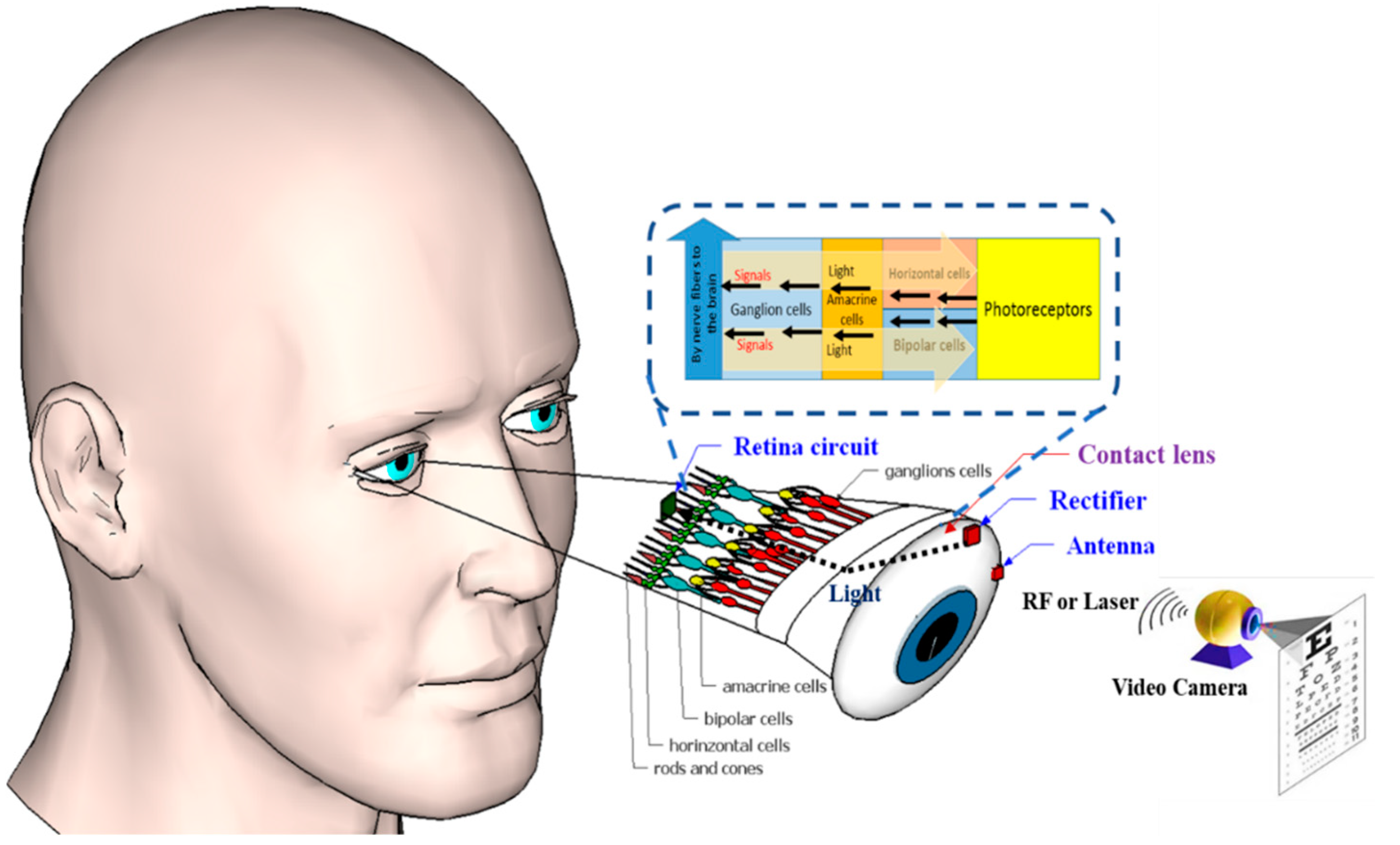
:1. Introduction
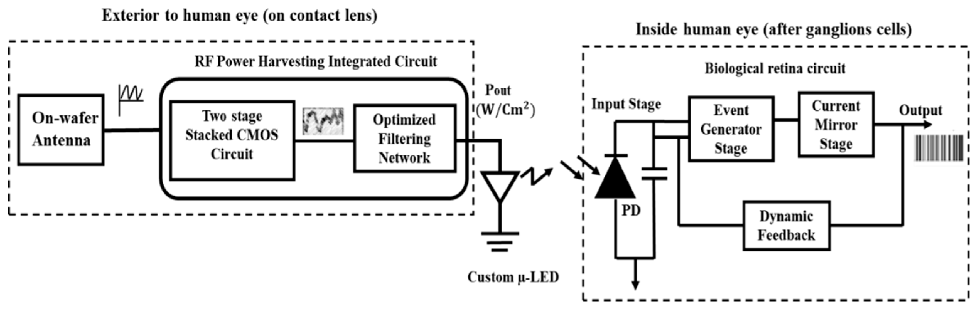
2. Design and Implementation
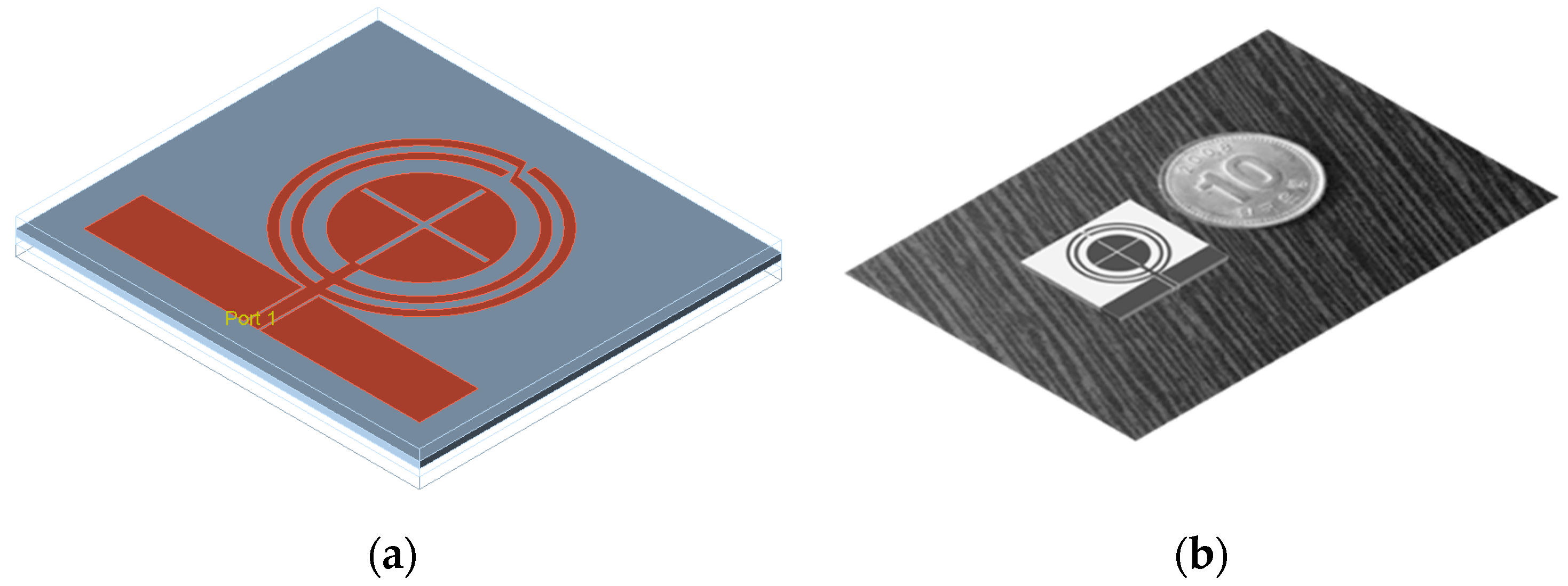
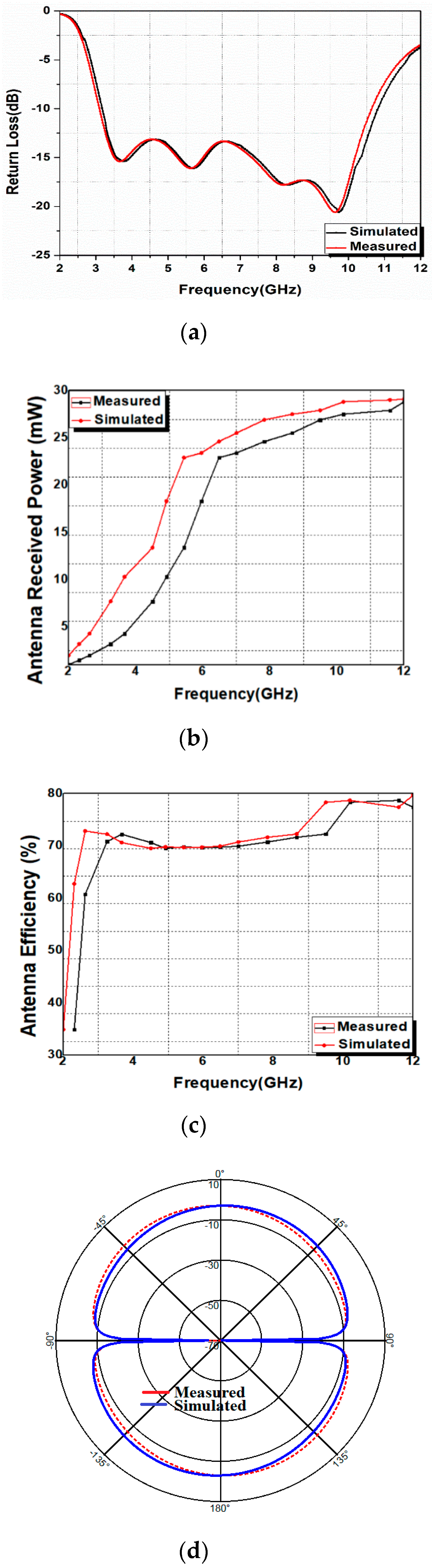
2.1. Antenna Design-I with Performance Evaluation
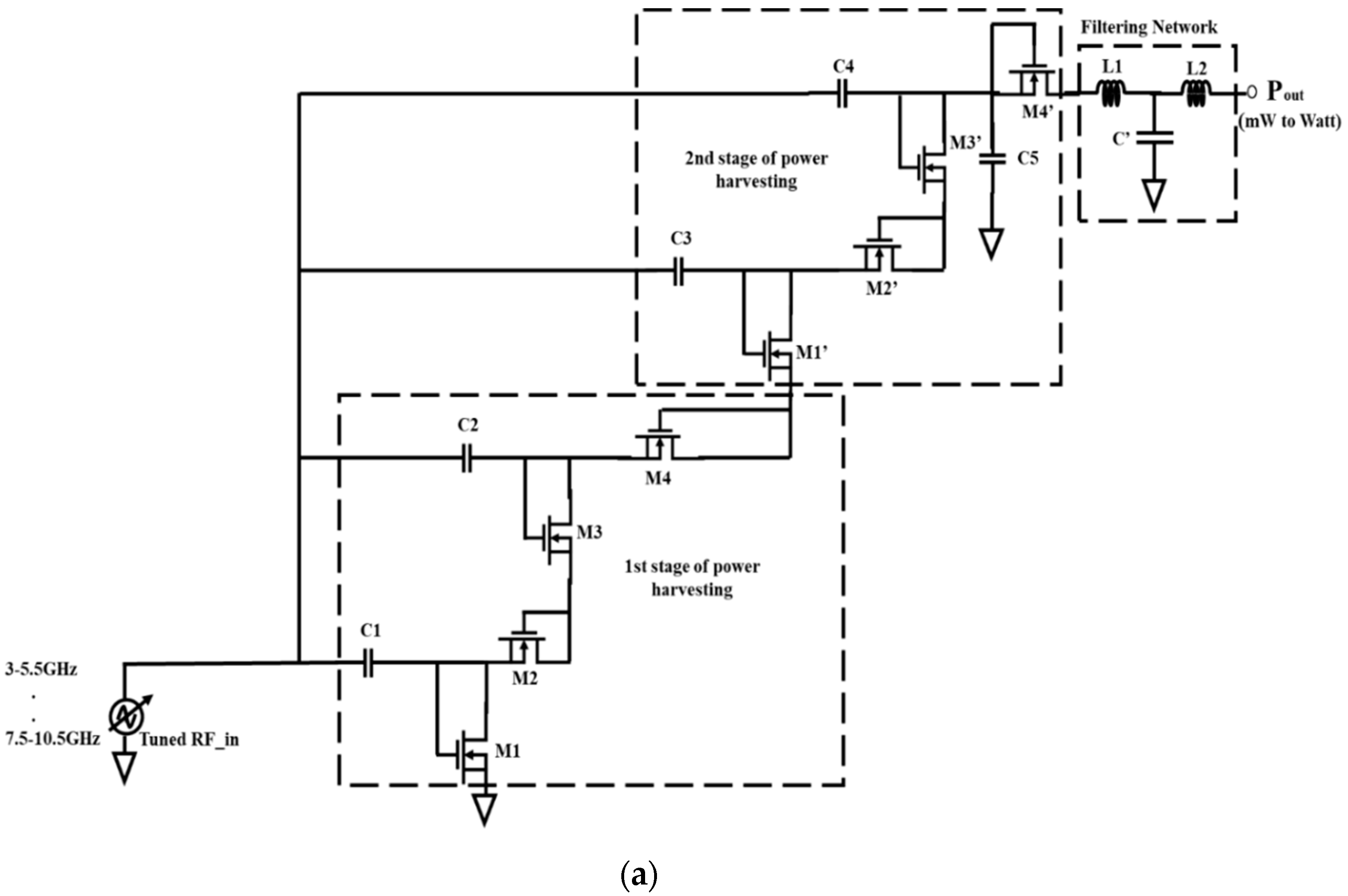
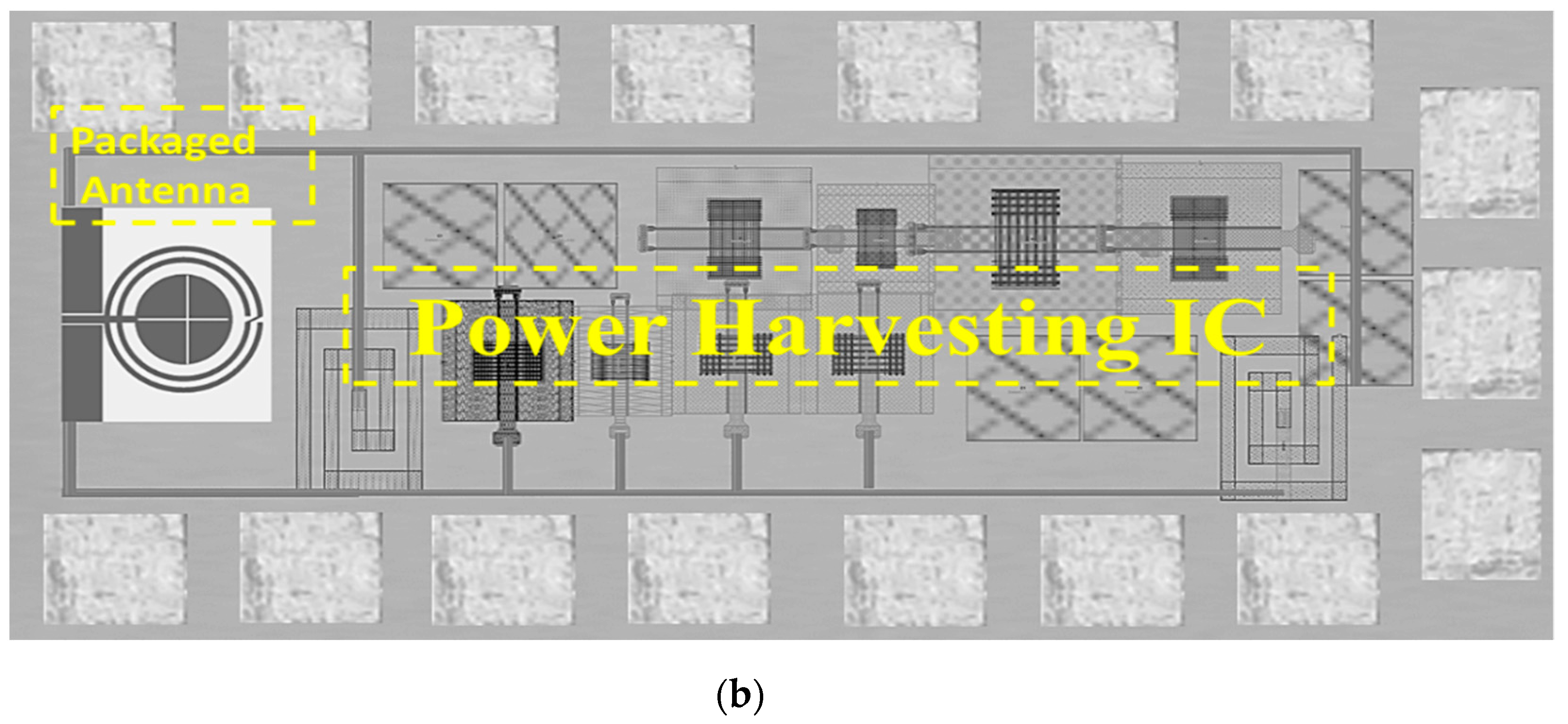
2.2. RF Power Harvesting Design-II
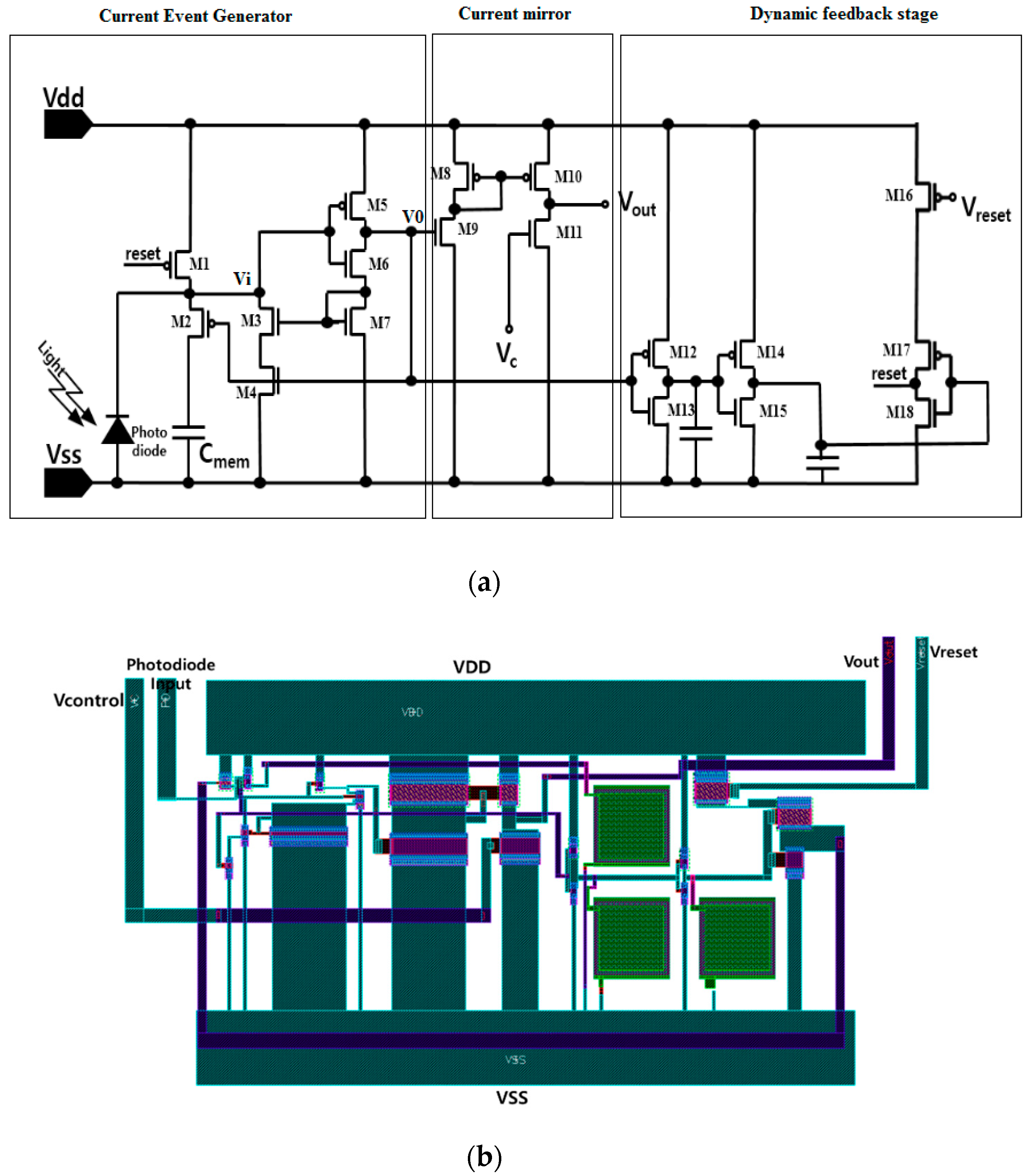
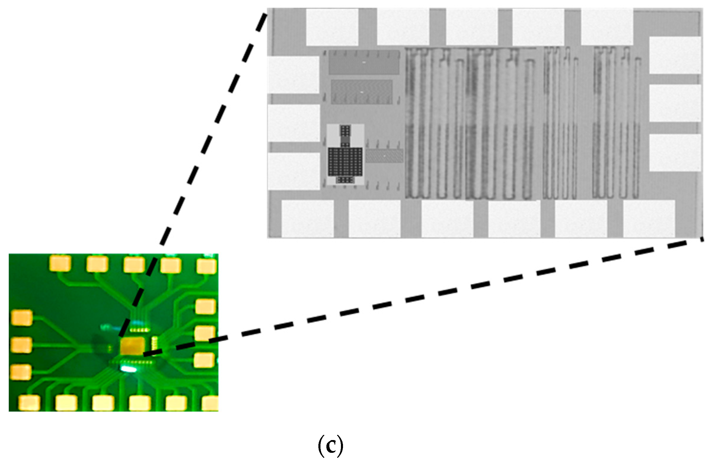
2.3. CMOS Retina Neuron IC: Design-III
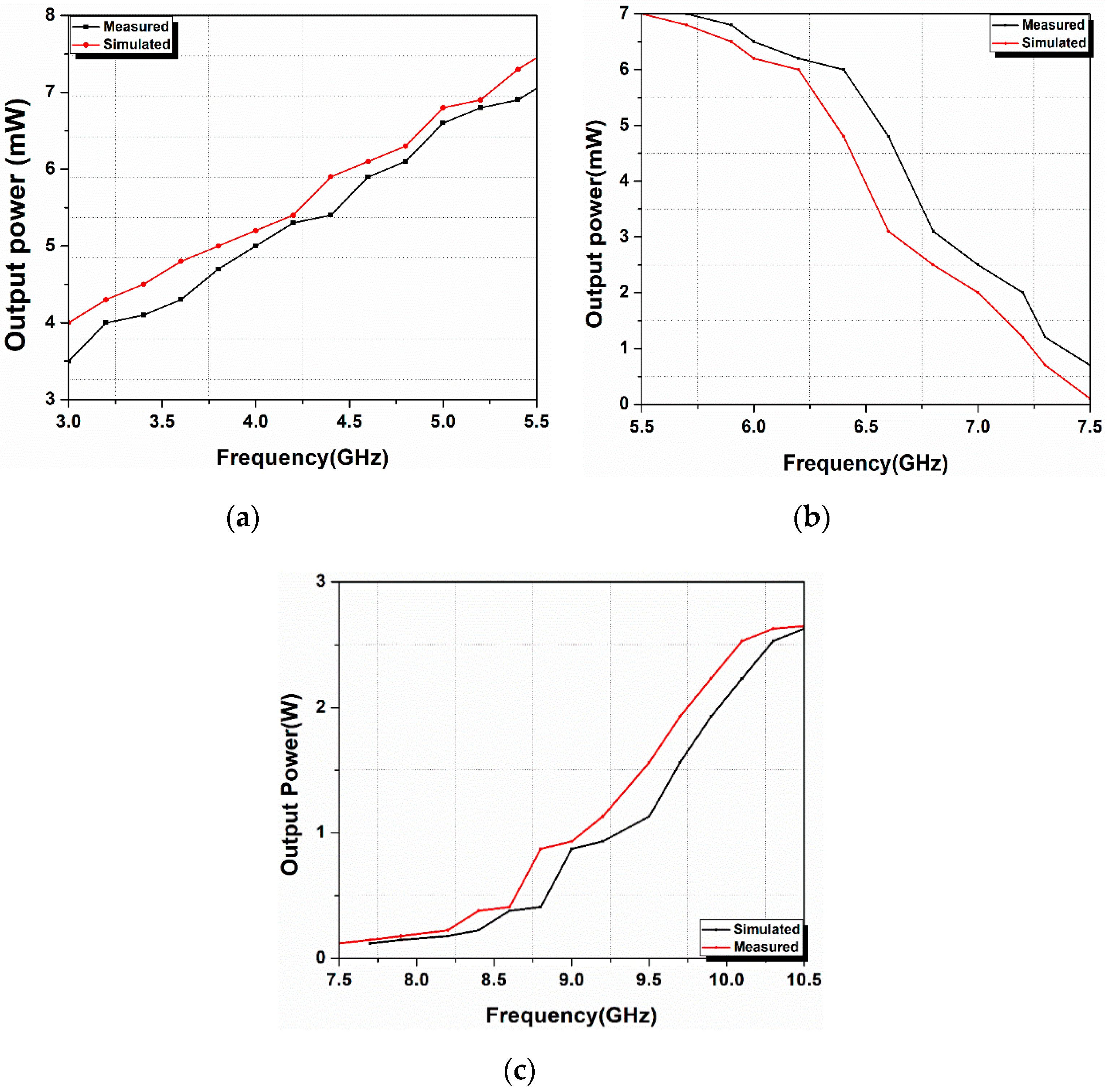
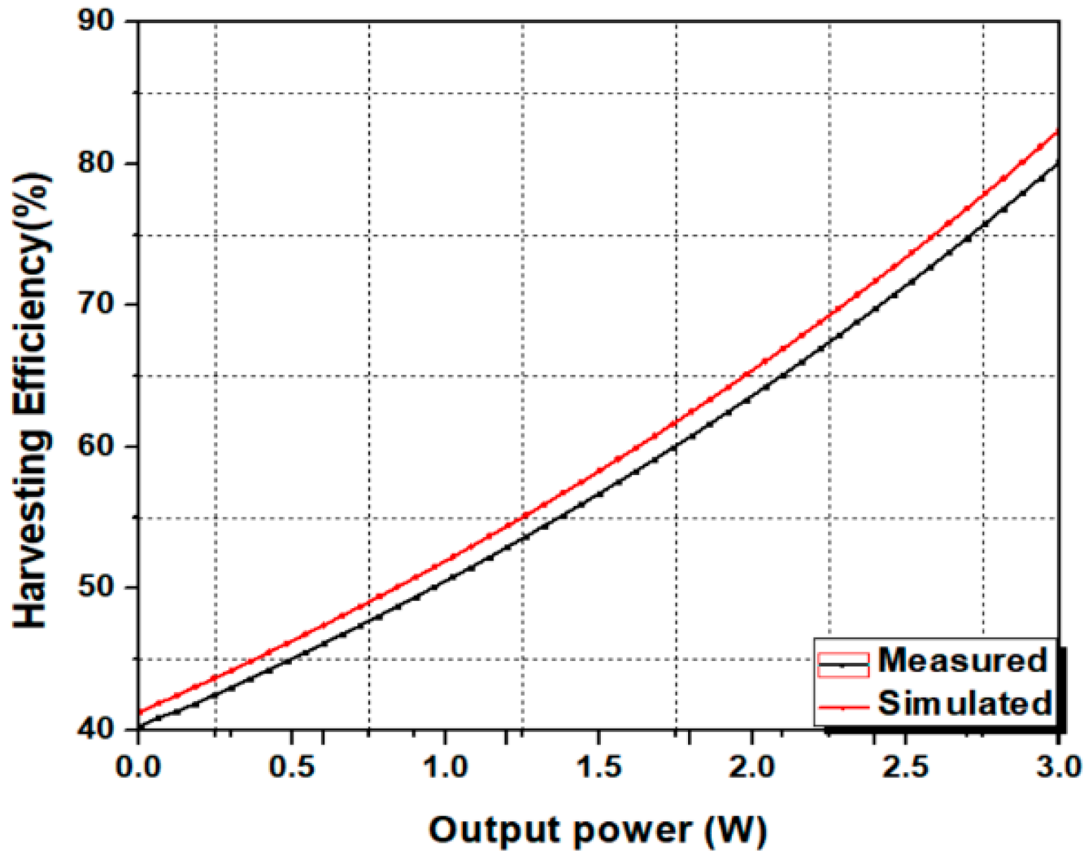
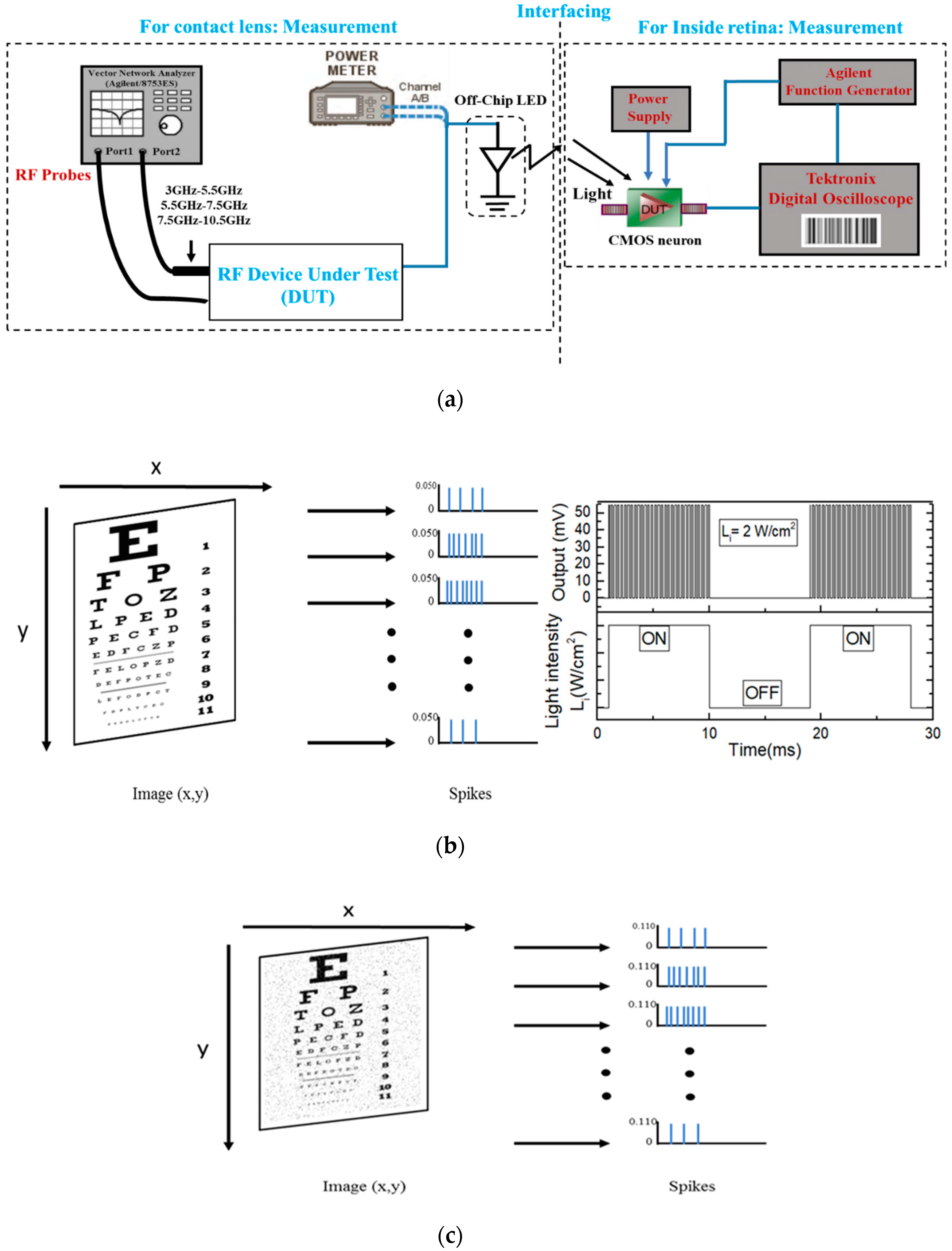
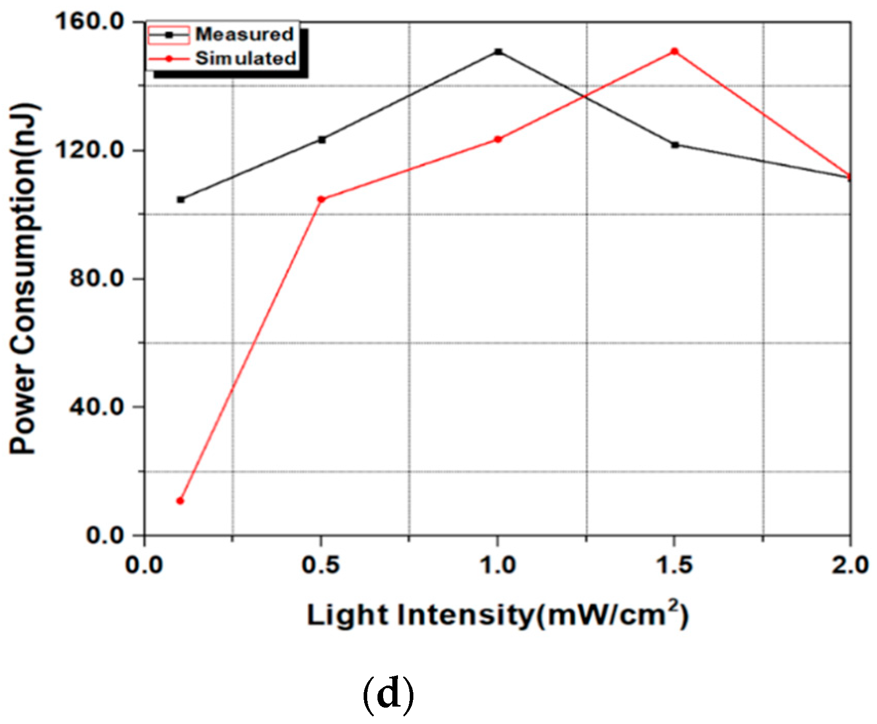
3. Results and Discussion
4. Conclusions
Author Contributions
Funding
Conflicts of Interest
References
- Mathieson, K.; Loudin, J.; Goetz, G.; Huie, P.; Wang, L.; Kamins, T.I.; Galambos, L.; Smith, R.; Harris, J.S.; Sher, A.; et al. Photovoltaic retinal prosthesis with high pixel density. Nat. Photon. 2012, 6, 391–397. [Google Scholar] [CrossRef] [PubMed]
- Lane, S.S.; Kuppermann, B.D. The implantable miniature telescope for macular degeneration. Curr. Opin. Ophthalmol. 2006, 17, 94–98. [Google Scholar] [CrossRef] [PubMed]
- Al-Shidaifat, A.; Kumar, S.; Song, H.-J. Voltage regulation of retina neuron model with dynamic feedback for biological acquisition image. BioChip J. 2017, 11, 300–307. [Google Scholar] [CrossRef]
- Wang, G.; Liu, W.; Sivaprakasam, M.; Kendir, G.A. Design and analysis of an adaptive transcutaneous power telemetry for biomedical implants. IEEE Trans. Circuits Syst. I Regul. Pap. 2005, 52, 2109–2117. [Google Scholar] [CrossRef]
- Ghovanloo, M.; Najafi, K. A modular 32-site wireless neural stimulation microsystem. IEEE J. Solid-state Circuits 2004, 39, 2457–2466. [Google Scholar] [CrossRef]
- Akin, T.; Najafi, K.; Bradley, R. A wireless implantable multichannel digital neural recording system for a micromachined sieve electrode. IEEE J. Solid-State Circuits 1998, 33, 109–118. [Google Scholar] [CrossRef] [Green Version]
- Liu, W.; Humayun, M.S. Retinal prosthesis. In Proceedings of the IEEE International Solid-State Circuits Conference Digest Technical Papers, San Francisco, CA, USA, 15–19 February 2004; IEEE: Piscataway Township, NJ, USA, 2004; pp. 218–219. [Google Scholar]
- Ortmanns, M.; Rocke, A.; Gehrke, M.; Tiedtke, H.-J. A 232-channel epiretinal stimulator ASIC. IEEE J. Solid-State Circuits 2007, 42, 2946–2959. [Google Scholar] [CrossRef]
- Chen, K.; Yang, Z.; Hoang, L.; Weiland, J.; Humayun, M.; Liu, W. An integrated 256-channel epiretinal prosthesis. IEEE J. Solid State Circuits 2010, 45, 1946–1956. [Google Scholar] [CrossRef]
- Kelly, S.K.; Shire, D.B.; Chen, J.; Doyle, P.; Gingerich, M.D.; Cogan, S.F.; Drohan, W.A.; Behan, S.; Theogarajan, L.S.; Wyatt, J.L.; et al. A hermetic wireless subretinal neurostimulator for vision prostheses. IEEE Trans. Biomed. Eng. 2011, 58, 3197–3205. [Google Scholar] [CrossRef] [PubMed] [Green Version]
- Chakrabartty, S.; Acharjee, S.; Al-Shidaifat, A.; Biswas, M.; Song, H. Gd-Doped HfO 2 Memristor Device, Evaluation Robustness by Image Noise Cancellation and Edge Detection Filter for Neuromorphic Computing. IEEE Access 2019, 7, 157922–157932. [Google Scholar] [CrossRef]
- Jung, L.H.; Shany, N.; Lehmann, T.; Preston, P.; Lovell, N.H.; Suaning, G.J. Towards a chip scale neurostimulator: System architecture of a current-driven 98 channel neurostimulator via a two-wire inter-face. In Proceedings of the International Conference IEEE Engineering in Medicine and Biology Society, Boston, MA, USA, 30 August–3 September 2011; IEEE: Piscataway Township, NJ, USA, 2011; pp. 6737–6740. [Google Scholar]
- Zrenner, E.; Bartz-Schmidt, K.U.; Benav, H.; Besch, D.; Bruckmann, A.; Gabel, V.-P.; Gekeler, F.; Greppmaier, U.; Harscher, A.; Kibbel, S.; et al. Subretinal electronic chips allow blind patients to read letters and combine them to words. Proc. R. Soc. B Biol. Sci. 2010, 278, 1489–1497. [Google Scholar] [CrossRef] [PubMed]
- Tokuda, T.; Takeuchi, Y.; Sagawa, Y.; Noda, T.; Sasagawa, K.; Nishida, K.; Fujikado, T.; Ohta, J. Development and in-vivo demonstration of CMOS-based multichip retinal stimulator with simultaneous multisite stimulation capability. IEEE Trans. Biomed. Circuits Syst. 2010, 4, 445–453. [Google Scholar] [CrossRef] [PubMed]
- Chen, K.; Lo, Y.-K.; Liu, W. A 37.6mm2 1024-channel high-compliance voltage SoC for epiretinal prostheses. In Proceedings of the IEEE International Solid-State Circuits Conference Digest Technical Papers, San Francisco, CA, USA, 17–21 February 2013; IEEE: Piscataway Township, NJ, USA, 2013; pp. 294–295. [Google Scholar]
- Al-Shidaifat, A.; Chakrabartty, S.; Kumar, S.; Acharjee, S.; Song, H. A Novel Characterization and Performance Measurement of Memristor Devices for Synaptic Emulators in Advanced Neuro-Computing. Micromachines 2020, 11, 89. [Google Scholar] [CrossRef] [PubMed] [Green Version]
- Monge, M.; Raj, M.; Honarvar-Nazari, M.; Chang, H.C.; Zhao, Y.; Weiland, J.; Humayun, M.; Tai, Y.; Emami-Neyestanak, A. A fully intraocular 0.0169 mm2/pixel 512-channel self-calibrating epiretinal prosthesis in 65nm CMOS. In Proceedings of the IEEE International Solid-State Circuits Conference Digest Technical Papers, San Francisco, CA, USA, 17–21 February 2013; IEEE: Piscataway Township, NJ, USA, 2013; pp. 296–297. [Google Scholar]
- Mokwa, W.; Goertz, M.; Koch, C.; Krisch, I.; Trieu, H.-K.; Walter, P. Intraocular epiretinal prosthesis to restore vision in blind humans. In Proceedings of the International Conference IEEE Engineering in Medicine and Biology Society, Vancouver, BC, Canada, 20–25 August 2008; IEEE: Piscataway Township, NJ, USA, 2008; pp. 5790–5793. [Google Scholar]
- Leonardi, M.; Leuenberger, P.; Bertrand, D.; Bertsch, A.; Renaud, P. A soft contact lens with a MEMS strain gage embedded for intraocular pressure monitoring. In Proceedings of the 12th International Conference on Solid-State Sensors, Actuators and Microsystems. Digest of Technical Papers, Boston, MA, USA, 8–12 June 2003; IEEE: Piscataway Township, NJ, USA, 2003; Volume 2, pp. 1043–1046. [Google Scholar]
- Stangel, K.; Kolnsberg, S.; Hammerschmidt, D.; Hosticka, B.; Trieu, H.; Mokwa, W. A programmable intraocular CMOS pressure sensor system implant. IEEE J. Solid-State Circuits 2001, 36, 1094–1100. [Google Scholar] [CrossRef]
- Cong, H.; Pan, T. Microfabrication of conductive PDMS on flexible substrates for biomedical applications. In Proceedings of the IEEE International Conference Nano/Micro Engineered and Molecular Systems, Shenzhen, China, 5–8 January 2009; IEEE: Piscataway Township, NJ, USA, 2009; pp. 731–734. [Google Scholar]
- Jow, U.-M.; Ghovanloo, M. Optimization of data coils in a multiband wireless link for neuroprosthetic implantable devices. IEEE Trans. Biomed. Circuits Syst. 2010, 4, 301–310. [Google Scholar]
- Chae, M.S.; Yang, Z.; Yuce, M.R.; Hoang, L.; Liu, W. A 128-channel 6mW wireless neural recording IC with spike feature extraction and UWB transmitter. IEEE Trans. Neural Syst. Rehabil. Eng. 2009, 17, 312–321. [Google Scholar] [CrossRef] [PubMed]
- Zamani, H.; Mohseni, P. A high-speed circuit architecture for IR-UWB transmission off ast-scan cyclic voltammetry in 0.35µm CMOS. In Proceedings of the IEEE Annual International Conference Engineering in Medicine and Biology Society, Buenos Aires, Argentina, 30 August–4 September 2010. [Google Scholar]
- Razavi, B. Design of Analog CMOS Integrated Circuits; McGraw-Hill: New York, NY, USA, 2000. [Google Scholar]
- Balint, P.; Kasabov, N.; Kiss, R.M. Selection and optimization of temporal spike encoding methods for spiking neural networks. IEEE Trans. Neural Netw. Learn. Syst. 2019, 31, 358–370. [Google Scholar]
- Lo, Y.; Chen, K.; Gad, P.; Liu, W. A Fully-Integrated High-Compliance Voltage SoC for Epi-Retinal and Neural Prostheses. IEEE Trans. Biomed. Circuits Syst. 2013, 7, 761–772. [Google Scholar] [PubMed]
- Kang, H.; Abbasi, W.H.; Kim, S.-W.; Kim, J. Fully Integrated Light-Sensing Stimulator Design for Subretinal Implants. Sensors 2019, 19, 536. [Google Scholar] [CrossRef] [PubMed] [Green Version]

| Component | Dimension |
|---|---|
| M1 | 40/0.18 µm |
| M2 | 23.5/0.18 µm |
| M3 | 112/0.18 µm |
| M4 | 58/0.18 µm |
| M1′ | 38/0.18 µm |
| M2′ | 23.5/0.18 µm |
| M3′ | 10/0.18 µm |
| M4′ | 28/0.18 µm |
| C1 | 46 pF |
| C2 | 10 pF |
| C3 | 12 pF |
| C4 | 80 pF |
| C5 | 20 fF |
| L1 | 0.5 nH |
| L2 | 0.267 nH |
| C’ | 112 fF |
| Design-I, II & III | Current Work | [27] | [28] |
|---|---|---|---|
| CMOS process (µm) | 0.065 | 0.18 | 0.35 |
| UWB Antenna | Bio-compatible telemetry Frequency range = 3.1 GHz to 10.7 GHz Data rate = 2 Mpbs | DPSK data telemetry Data rate = 2 Mpbs | - |
| RF Power harvesting IC | On-chip transistor, L.V Efficiency = 40% to 80% | On-chip transistor, H.V | - |
| CMOS neuron retina | SoC (System on a chip) Chip area = 1.1 × 2.1 mm2 Power consumption = 110 nW | SoC Chip area = 5.7 × 6.6 mm2 | SoC Chip area = 4.3 × 3.2 mm2 |
| Application | Retinal Image Acquisition | Epi-Retinal and Neural Prostheses | Subretinal Implants |
© 2020 by the authors. Licensee MDPI, Basel, Switzerland. This article is an open access article distributed under the terms and conditions of the Creative Commons Attribution (CC BY) license (http://creativecommons.org/licenses/by/4.0/).
Share and Cite
Al-Shidaifat, A.; Kumar, S.; Chakrabartty, S.; Song, H. A Conceptual Investigation at the Interface between Wireless Power Devices and CMOS Neuron IC for Retinal Image Acquisition. Appl. Sci. 2020, 10, 6154. https://doi.org/10.3390/app10186154
Al-Shidaifat A, Kumar S, Chakrabartty S, Song H. A Conceptual Investigation at the Interface between Wireless Power Devices and CMOS Neuron IC for Retinal Image Acquisition. Applied Sciences. 2020; 10(18):6154. https://doi.org/10.3390/app10186154
Chicago/Turabian StyleAl-Shidaifat, AlaaDdin, Sandeep Kumar, Shubhro Chakrabartty, and Hanjung Song. 2020. "A Conceptual Investigation at the Interface between Wireless Power Devices and CMOS Neuron IC for Retinal Image Acquisition" Applied Sciences 10, no. 18: 6154. https://doi.org/10.3390/app10186154
APA StyleAl-Shidaifat, A., Kumar, S., Chakrabartty, S., & Song, H. (2020). A Conceptual Investigation at the Interface between Wireless Power Devices and CMOS Neuron IC for Retinal Image Acquisition. Applied Sciences, 10(18), 6154. https://doi.org/10.3390/app10186154