Featured Application
The contribution of this paper is to propose a dual-stream convolutional neural network (CNN) using two solder regions for inspections of surface mount technology (SMT) assembly defects. We extract two solder regions from a printed circuit board (PCB) image and input them to a dual-stream CNN that is constructed for defect classification. The proposed method helps manufacturers efficiently classify and manage defects in an automatic optical inspection system in the SMT line. In addition, since the proposed method uses the solder region for inspection, it can be applied to the inspection of all components having a solder region mounted on the PCB.
Abstract
The automated optical inspection of a surface mount technology line inspects a printed circuit board for quality assurance, and subsequently classifies the chip assembly defects. However, it is difficult to improve the accuracy of previous defect classification methods using full chip component images with single-stream convolutional neural networks due to interference elements such as silk lines included in a printed circuit board image. This paper proposes a late-merge dual-stream convolutional neural network to increase the classification accuracy. Two solder regions are extracted from a printed circuit board image and are input to a convolutional neural network with a merge stage. A new convolutional neural network structure is then proposed that is able to classify for defects. Since defect features are concentrated in solder regions, the classification accuracy is increased. In addition, the network weight is reduced due to a reduction of the input data. Experimental results for the proposed method show a 5.3% higher performance in F1-score than a single-stream convolutional neural network based on full chip component images.
1. Introduction
Surface mount technology (SMT) is a manufacturing method used to produce electronic circuits by assembling components onto the surface of a printed circuit board (PCB). Using SMT, solder paste is applied to the surface of a circuit board, a surface mount component (SMC) is installed, and the solder is then melted to produce the PCB. The automated optical inspection (AOI) machine of an SMT line inspects for assembly defects in the PCB, using a camera and classifies defects according to type. After classification, defects are used for maintenance tasks to identify root causes in the assembly and to improve the process sequence. In recent years, 3D AOI has become widespread, although 2D AOI remains commonly used due to its high economic efficiency.
Figure 1 shows a defect in a SMT assembly line obtained using a light-emitting diode (LED) light system. SMT assembly defects can occur either in the package or in the solder region. The defect is labeled as missing when the chip component is not in place according to the PCB design. The Manhattan defect occurs when the chip component is erected horizontally, and the Tombstone defect occurs when the chip component stands vertically on one solder, with the other side being separated from the solder. An over-soldering defect occurs when the amount of solder is higher than normal; an under-soldering defect occurs when the solder is less than a normal defect. The missing component, Manhattan defect and Tombstone defect can be considered package defects, while over-soldering and under-soldering are defects in the solder region.
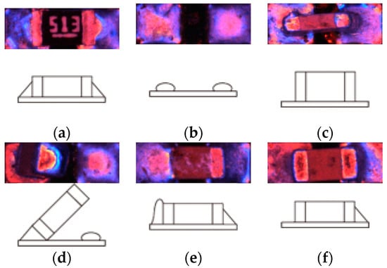
Figure 1.
Defects in the surface mount technology (SMT) assembly line: (a) normal (b) missing (c) Manhattan (d) Tombstone (e) over-solder, and (f) under-solder.
Two-dimensional AOI-based inspection methods include printed circuit board inspection, component detection, and defect classification [1,2,3,4,5,6,7,8,9,10,11,12,13,14,15,16]. In this paper, the defect classification method in the SMT line can be divided into non-learning-based and learning-based methods. Non-learning-based defect classification compares the threshold values of the template, features, and so on [4,5,6,7,8,9]. For instance, H. Xie [4] proposed a defect classification method using the difference in images between the input image and the reference image. First, the variance of gray of each defect is obtained from the training image dataset. Then, differences between a reference image for each defect and the input image are obtained. H. Xie [4] classified defects by comparing the differences between images and the variance of gray of each defect. H. Wu [5] proposed a method for discriminating defects by extracting a chip component region. They segmented the chip electrode region by applying the Otsu binarization algorithm to the red color channel of the chip component image. They first extracted the vertical projection and horizontal projection histograms from the binarized image, and then extracted the location of the chip component using the gradient of the vertical and horizontal projection histograms. Defect identification is performed by comparing the extracted chip component’s location with the PCB design. F. Wu [6] proposed a method for classifying defects in IC chip leads. They divided the IC chip leads into subregions and obtained the ratio and center of gravity of the highlight regions from each subregion. A highlight region is a set of pixels above a certain pixel threshold in a subregion. Each subregion and its features are defined as ‘logical features’. A decision tree based on logical features is then used to classify defects.
Learning-based methods classify defects through features such as the average pixel value of each red, green and blue (RGB) channel and the highlight value of each RGB channel [10,11,15,16], and normalized-cross-correlation (NCC) [10,11] extracted from massive chip component defect datasets obtained using an LED light system. The model analyzes and learns these features then classifies the new input data [10,11,12,13,14,15,16]. H. Wu [10] proposed a Bayesian classifier and support-vector machine (SVM)-based defect classification method. They extracted the features described above from the solder region and classified them using a Bayesian classifier and SVM. The chip components were first classified as either normal or non-normal using Bayesian classifier, and the defect type of non-normal was classified using SVM. F. Wu [12] proposed a defect classification method using color grades, to be used in conjunction with features of the above method. The color grades that describe the color sequence from one side to the other in a pointed region have different RGB patterns depending on the defect. They improved defect classification performance using color grades and decision trees. While the learning-based classification method generates a complex and detailed model considering the accumulated data, the non-learning-based method simply compares thresholds such as an NCC of template matching. Similarly, H. Wu [11] proposed a classification model that uses the loss of multilayer perceptron (MLP) in the genetic algorithm to select optimal features. Song [15] further segmented the image into detailed regions to extract the features within. They specified nine subregions by considering the structure of the chip component. They extracted the average pixel value of each RGB channel and the highlight value of each RGB channels from the subregion. They then used the MLP to classify the defects found.
Learning-based methods are a recent advance in the field of defect classification. In particular, convolutional neural network (CNN) specialize in visual imagery; they are used in fields such as object detection, classification [17,18,19,20], and defect detection [21,22,23]. Q. Xie et al., [21] proposed a two-level hierarchical CNN system for the inspection of sewer defects. A normal-defect labeling CNN first classifies the input image as other than normal, and the inter-defect labeling CNN then classifies types of defects other than normal. The normal-defect labeling CNN classifies the input image into two types, normal and abnormal, and the inter-defect labeling CNN classifies the abnormal defect types. In terms of system structure, the method of Q. Xie [21] can be said to be similar to that of H. Wu [10]. H. Yang [23] subsequently proposed a multi-scale feature clustering autoencoder (MS-FCAE) for the defect inspection of fabrics and metal surfaces. They detected defects using the differences between the original images and the image restored image using an autoencoder. They improved the accuracy of defect detection by increasing the restoration performance of the autoencoder using clustering on the latent vector.
A number of studies that use CNN to classify defects in a surface mount device (SMD) assembly [24,25] currently exist. For example, N. Cai [24] proposed a cascaded CNN for the detection of soldering defects. The solder region of a chip component was divided into several regions, and the CNN corresponding to these regions were connected. Defects were then classified based on the output of the CNN. However, these methods were only able to detect defects occurring in the solder region, and not in the package region. Although previous methods could determine whether there was a defect or not, they were unable to classify defects by type. Y. G. Kim [25] proposed a CNN that could detect and classify defects in both the soldering and package region using a single-stream CNN. However, the chip component image included the silk line background, which is unnecessary for defect classification. Therefore, this model can become inefficient as it includes irrelevant items in the image. In addition, the single-stream CNN-based defect classification model uses the full chip component image. This input image contains background that is not related to the defect of chip components, such as silk lines and circuit patterns. As such, in the training step, the weight of the convolution layer for the background can be higher than the weight of the actual defect region. In this case, there is a possibility that the CNN model will overfit the training dataset.
This paper proposes a new dual-stream CNN using two solder regions in the chip component image. It has a parallel stream-based CNN, and they merge after their own processing steps, as most defects feature in the chip component are included in the solder regions. For example, missing defects can be distinguished by the presence or absence of electrodes in the solder region. Tombstone and Manhattan defects can also be distinguished by the size of the solder region. Therefore, the proposed method can detect both soldering and packaging defects. We then used a merge step to combine the results of the dual-stream CNN. Merging refers to the process of combining two streams into one stream, as the proposed method uses a multiple-input single-output (MISO) structure in which two solder regions are used as the input and one defect type as the output. After the merge, the convolution layer is found. Through the convolution operation, the feature map having a high weight is transferred to the bottom layer, and the feature map having a low weight disappears during inference. This series of steps is similar to a kind of feature section. Here, merging is classified into two types: early merge and late merge. An early merge means performing the merge at the convolution layer level. The output feature map of the convolution layer, which is the front part of the CNN, is a low-level feature. Early merge combines the low-level feature map output from the convolution layer of each stream into one feature map. Late merge means performing the merge in the fully connected layer stage. The output feature map of the fully connected layer is a high-level feature because the fully connected layer is located at the end of the CNN. Late merge combines the high-level feature map output from the fully connected layer of each stream into one feature map.
The contributions of this paper can be summarized as follows:
- We propose an inspection method that is optimized for classifying chip component defects using two solder regions. We propose a system that extracts features by dividing two solder region images into each stream.
- We present experimental results according to the merge structure in a dual-stream CNN. We propose a CNN structure that is optimized for the defect classification of chip components by comparing an early-merge method in which the merge is performed in the convolution layer with a late-merge method in the fully connected layer.
- In terms of the chip defect classification, the proposed method achieves a higher accuracy and F1-score than a single-stream CNN based on the full chip component image.
The structure of this paper is as follows. Section 2 defines the assembly defect classification problem and Section 3 illustrates the light system used in this paper. Section 4 describes the structure of the assembly defect classification system. Section 5 describes the algorithm used for extracting the solder regions. Section 6 describes the proposed CNN structure. Section 7 presents the results of the experiments and analyzes their accuracy. Finally, Section 8 summarizes this paper.
2. Problem Definition
In this paper, the chip component consists of two solder regions and a package region, including a chip capacitor, chip diode, chip register, and tantalum capacitor. Figure 2a shows an image of these components. Chip capacitors, diodes, chip resistance, and tantalum capacitors are in order from the left. Components vary in size from 0.6 mm × 0.3 mm to 3.2 mm × 1.6 mm. Figure 2b shows the structure of the chip component, consisting of two solders and one package.
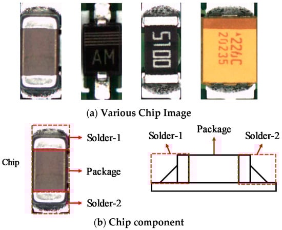
Figure 2.
Chip components: (a) various chip components mounted on the printed circuit board (PCB), (b) top view (left) and side view (right) of chip component.
Each pixel vector of the image input from the illumination system includes red, green, and blue pixel values.
The chip component image is defined as:
The channel image for each color channel of chip component image , , is expressed as a matrix.
For the defect types, the defect type number is defined as . Then, the set of defect types is as follows.
3. Light-Emitting Diode (LED) Light System
Figure 3 shows the dome-type illumination system. The system is used to obtain chip component images from the PCB. The illumination system has three colored LEDs: the red lights positioned vertically emphasize the flat area of the component, and the blue lights placed horizontally illuminate the beveled area of the component. The green lights emphasize the soft area of the component. Each light has a different irradiation angle; therefore, the color value is different according to the gradient of the surface. In the chip component image, the closer to red, the larger the gradient; and the closer to blue, the lower the gradient. We can then use the color value of the chip component image as gradient information. We can also indirectly infer the height of the chip components through this gradient.
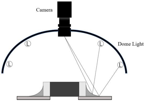
Figure 3.
Red, green and blue (RGB) light system using light-emitting diode (LED) lights.
4. System Structure
SMT assembly defects can be classified by CNN, a deep neural network that has shown high performance in image recognition and processing. Figure 4 shows the structures of CNN for SMT assembly defect classification. In both cases, the probability of the occurrence of each defect type can be obtained. The defect type for the input image is defined as:
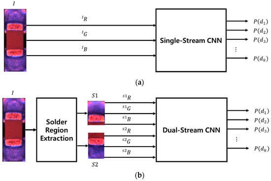
Figure 4.
Input and output structures of convolutional neural networks (CNNs) for defect classification: (a) single-stream CNN; (b) dual-stream CNN.
Figure 4a is an assembly defect classification system having a single-stream CNN that uses the color channel images (, , and ) of each chip component image as inputs. Although the chip component image includes both the package and solder regions, it cannot exclude the silk line background. Figure 5 shows the PCB patterns included in the background region of the chip component image.
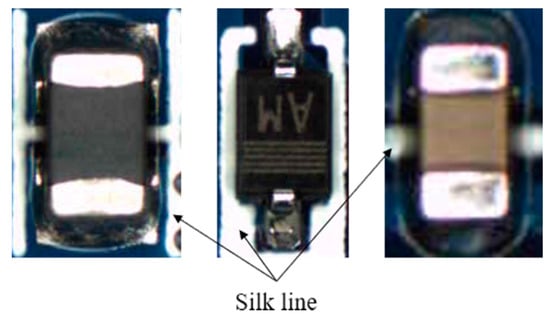
Figure 5.
PCB background patterns in chip component images. The silk line is printed on the PCB to provide additional information about the component. Silk lines can adversely affect defect classifications because of their similarity to solder region.
Figure 4b shows the structure of the assembly defect classification system with the dual-stream CNN. The inputs included the two solder region images ( and ) extracted from the chip component image , and the color channel image (, , and ; and , , and ). Note that the solder region image does not include the silk line, which disrupts the feature extraction of CNN.
As described in the Introduction, most defect features are distributed in the solder region in the component, and as such the two solder regions can be used to classify both the package and solder defects. Figure 6 shows the solder region image based on defect type, wherein the defect feature is distributed in the solder region. Removing unnecessary PCB patterns can reduce the chance of misclassification in solder region extraction, and thereby increase its accuracy. In addition, the size of the chip component image can also be reduced. This optimization simplifies the CNN internal structure, reducing the overall weight capacity and computational time.
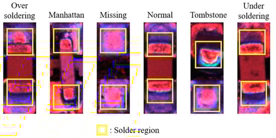
Figure 6.
Solder region of chip image. The solder region has different shapes according to the defect type. In the above images, the closer the pixel value is to red, the flatter the slope, and the closer to blue, the smoother the slope. It is easy to classify the defect by only considering the solder region of the chip image, because the defect features are gathered in the solder region. This is especially true for solder defects such as over-soldering and under-soldering.
5. Solder Region Extraction
Solder region extraction is the process of extracting the image of the solder region in each chip component image from the PCB image acquired by the camera.
5.1. Chip Component Region Extraction
To extract the chip component image from the PCB image, we first need the position and size of each component. The Gerber format is commonly used for PCB manufacturing, but it can also be used to extract the location and size of the solder regions for each chip component [26]. The chip component image extraction process occurs in three steps: the PCB image and the solder region data from the Gerber format is loaded; the solder region for each chip component is merged and the chip component region is then obtained by extending the ratio to the merged region; and the chip component image corresponding to each chip component region from the PCB image is finally extracted.
Figure 7 shows the PCB image of a chip component consisting of the package region, solder region, silk line, and component. To detect assembly defects, the chip component region is set to an extended region rather than being limited to the solder region. The extended region includes various pattern images in the PCB, such as silk lines. This background is excluded in the solder region extraction step.
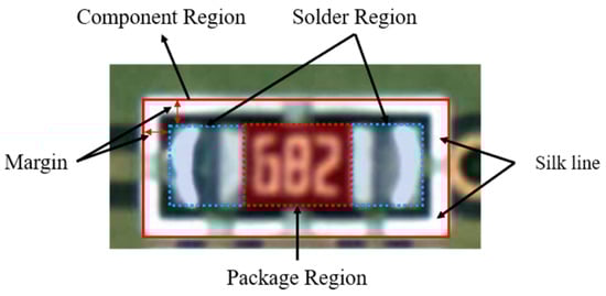
Figure 7.
Solder region of the chip component. The area marked with a blue square is the solder region, and the area, marked with a red square is the package region. The white area around the solder and package region is the silk line.
5.2. Solder Region Extraction
First, the chip component image , an RGB image, is converted into a grayscale image .
where,
The horizontal projection for is then obtained using Equation (8).
Figure 8a,b show the chip component image and horizontal projection of the chip component image, respectively. As the solder region of the chip component is brighter than the package region, the horizontal projection is divided into two regions: dark (middle) and bright (top and bottom).
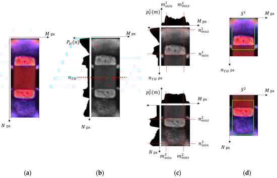
Figure 8.
Solder region extraction of SMT chip image where ‘px’ refers to pixels: (a) chip component image, (b) gray scale image showing horizontal split of chip component, (c) vertical and horizontal projections, and (d) result of solder region extraction.
From the horizontal projection, the split point () for dividing the chip component region into two regions is calculated. The split point is the coordinate of the n-axis (y-axis) that divides the chip component into two regions. As shown in Figure 6, normal chip components have similar vertical projection values both above and below. However, since defects such as under-solder, over-solder, and Tombstone have different color distributions in the upper and lower solder regions, it is necessary to divide the chip component into two regions for accurate solder region extraction. In the horizontal projection shown in Figure 8b, the chip component is divided into two regions. We then used the Otsu method [27] on the horizontal projection to obtain the threshold value and used it as the split point
Based on the split point, the horizontal projection is divided into and .
The vertical projection and for are also obtained.
Figure 8c shows the horizontal and vertical projections of the chip component image divided into dark and bright sections. In the figure, the region where the brightness value changes abruptly in each projection denotes the boundary of the solder region. Let the minimum and maximum values of the horizontal projection be (), respectively; and the minimum and maximum values of the vertical projection be (), respectively. The solder region () is then defined by Equation (11).
Figure 8d shows the solder region image extracted by the minimum and maximum values of the horizontal and vertical projections.
6. Convolutional Neural Network (CNN) Structure
CNN is a machine-learning method that generates a model by extracting and analyzing the features of the input image data. Commonly, a single-stream CNN that takes one image datum is used, but this paper will examine a dual-stream CNN that uses two solder regions as the input data.
6.1. Single-Stream CNN
Figure 9 shows the structure of a single-stream CNN. Most CNNs, such as AlexNet [28] and VGGNet [29], have a single-stream structure. The input data of the single-stream CNN consists of the , and channel image of the chip component image. Each color channel of the input data has a size of 64 × 64 pixels.
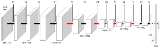
Figure 9.
Structure of a single-stream CNN.
In Figure 9, C#, P#, and R# represent a convolutional layer, max pooling layer, and ResBlock layer of Figure 10, respectively. The convolution layer C# has a kernel size of 3 × 3, padding = 1, and stride = 1. The max pooling layer P# has a kernel size of 2 × 2, padding = 0, and stride = 2. The ReLu function was used as the activation function of the convolution layer and the fully connected layer. Unless otherwise noted, the convolution layer and max pooling layer will have the same configuration.
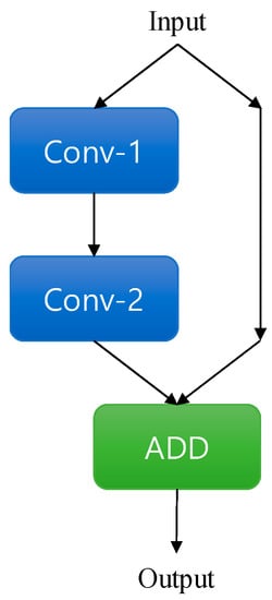
Figure 10.
ResBlock structure. ResBlock consists of two convolution layers: the output of the ResBlock is the sum of the input feature and the output of the last convolution layer.
First, for local feature extraction, the input data are converted into a feature map 64. × 64 × 64 in size through C1. After the initial conversion, the feature map is again converted into a 64 × 64 × 384 feature map through two convolution layers C2 and C3. The output feature map of C3 passes through C4, and then for global feature extraction scales down to 32 × 32 × 512 through the max pooling layer P1. It is converted into a feature map 16 × 16 × 512 in size through C5 and P2. To avoid the gradient-vanishing problem, ResBlock layers [30] R1 and R2, are attached at the rear of the network. R1 and R2 in Figure 10 show the structure of the ResBlock layers used in this paper. The feature map is converted into 8 × 8 × 512 size through R1 and P3, and 4 × 4 × 512 through R2 and P4. For the fully connected layer input, the feature map output of C6 passes through a 4 × 4 convolution layer C7 with padding = 0 and is converted to 1 × 1 × 512. A probability value for six types of defect is finally output through a fully connected layer having a size of 1 × 1 × 1024. Table 1 shows the detailed structure of the ResBlock layers R1 and R2 used in this paper.

Table 1.
Layer configuration of CNN.
The reason that our proposed method uses a 3 × 3 kernel size for the convolution layer is because the computational efficiency per receptive field is highest for this the kernel size. Since the computational power of the convolution layer is the sum of the product of the kernel weight and the input value, the computational power of the convolution layer is the square of the kernel size. For example, when the computation power of a 3 × 3 convolution layer is ; similarly, the computational power of a 5 × 5 convolution layer is . Two 3 × 3 convolution layers are required to have the same receptive field as a 5 × 5 convolution layer only using the 3 × 3 convolution layer. At this time, since the calculation of two 3 × 3 convolution layers is , the computational efficiency per receptive field is better than that of the 5 × 5 convolution layer. For these reasons, we used a 3 × 3 kernel size. We used padding because it maintains the size of the output feature map. With the 3 × 3 convolution layer, the size of the output feature map decreases. If padding size is set to ‘0′, the output has very small feature maps in the early stages of CNN. It will adversely affect the performance of CNN. Here, we set the padding size to ‘1′ to prevent degradation of CNN performance.
Common pooling methods include max pooling and average pooling. Max pooling selects the maximum value from the kernel, and average pooling calculates the average of the kernel values for pooling. In this paper, ReLu is used as the activation function, and a number of ‘0′ values are output due to the ReLu function. At this time, if average pooling is used, a down-scale weighting phenomenon occurs in which strong weights are reduced by the average operation, potentially leading to overall performance degradation in the model. Therefore, we used max pooling in the proposed method, which is less affected by down-scale weighting.
, , and are obtained by extending the solder region. The image size increases with the margin used, with the size of the single-stream CNN using it increasing proportionally. In addition, the extended regions of , , and include various background regions in the PCB such as the silk line. This may hinder the performance of the CNN since the background region is included in the defect classification.
6.2. Dual-Stream CNN
Dual-stream CNN generates a classification model using two solder images ( and ), which consist of the color channel image (, , and ; and , , and ). Figure 11 shows two different structure of dual-stream CNN. Each input datum has a size of 32 × 32 pixels. The output of the final stage of the dual-stream CNN is the probability value for each defect, similar to that of the single-stream CNN.
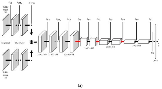
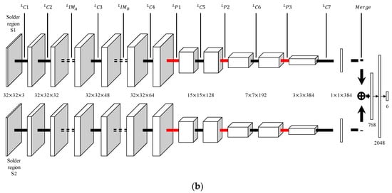
Figure 11.
Structures for dual-stream CNNs. (a) Early-merge dual-stream CNN. The merge is located at the convolution layer of the network. (b) Late-merge dual-stream CNN. The merge is located at the front of the fully connected layer.
The feature value is the output value extracted by calculating the weight and bias value in a layer included in a deep-learning network. The feature value for the input data in the CNN is defined by Equation (12).
where is the weight of the kernel, are the kernel sizes, σ is the activation function, and and are the location of the input data used to calculate the feature map. The feature matrix consists of output values of the deep-learning network in a 2D image. Let the kernel stride be , and padding be . The feature matrix is then defined as follows:
In general, the deep-learning network layer consists of a multichannel kernel. Therefore, the feature matrix is output in multiple channels called the feature map. Let the number of layers be , the number of kernels be , and the output feature matrix for each kernel be make up the feature map of the output layer .
Consequently, merging is the process of combining different feature maps into one map. To calculate for the merge result , let the number of kernels of the output layer be , and the feature map output from output layers with kernel channels be .
where,
By merging feature maps from different layers, multiple low-dimensional feature maps can be combined into a single high-dimensional feature map. This high-dimensional feature map can them be used to extract the global features directly related to defect classification, thereby improving the classification accuracy of the CNN model. Merging also simplifies the CNN layer by unifying feature maps, as dual-stream CNNs have a multi-stream structure with multiple layer branches. However, after merging, feature maps can be integrated into a single-stream structure with a single layer branch. Merging also reduces the weight of the CNN model by converting the CNN model from a two-stream structure to a single-stream structure.
6.2.1. Early-Merge Dual-Stream CNN
An early-merge dual-stream CNN is a network structure in which the merge is performed in front of the network (Figure 11a). In an early-merge dual-stream CNN, the input data is converted into 32 × 32 × 32 feature maps through . Each feature map output from passes through an inception module (IM) [31]. The IM has a wide reception field, as it combines convolution layers having various kernel sizes, allowing for efficient feature map extraction. and (Figure 12 and Table 1) represent the structure of the inception module used in this paper.
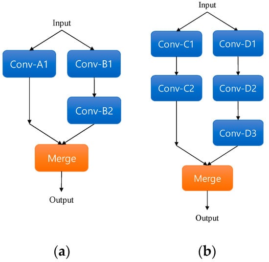
Figure 12.
Inception module (IM) structure: (a) structure of and layer, (b) structure of and layer.
Through merging, each 32 × 32 × 32 feature map extracted from the is transformed into a single feature map of 32 × 32 × 64. After extraction and transformation, the size of the feature map is converted to 32 × 32 × 48 through . The resulting feature map is of size 32 × 32 × 64 through . Through three convolution layers ( and ) and max pooling layers ( and ), the feature maps are sequentially converted to 15 × 15 × 192, 7 × 7 × 210, and 3 × 3 × 768. At the last convolution layer , the 3 × 3 × 768 feature map output through is converted into a 1 × 1 × 768 feature map for input into the fully connected layer.
6.2.2. Late-Merge Dual-Stream CNN
The difference between late-merge dual-stream CNN and early-merge dual-stream CNN is that late-merge dual-stream CNN merges immediately before the fully connected layer. Figure 11b shows the structure of a late-merge dual-stream CNN.
The input data of the late-merge dual-stream CNN are converted into a 32 × 32 × 32 feature map through the and convolution layer. The feature map then goes through two inception modules ( and ) and two convolution layers ( and ). The 32 × 32 × 64 feature map which is output from , which passes through convolution layers and and the max pooling layer and . Accordingly, the size of the feature map changes, in the order of 15 × 15 × 128, 7 × 7 × 192, and 3 × 3 × 384. In the last convolution layer , we transformed the feature map of each layer into a 1 × 1 × 384 feature map. After the last convolution layer, two 1 × 1 × 384 feature maps are merged to obtain a 1 × 1 × 768 feature map. The feature map output from the merge then proceeds to the fully connected layer.
The dual-stream CNN reduced the weight of the network via the smaller input data size in comparison to single-input CNN. The actual solder region is smaller than 32 × 32 pixels. However, input data less than 32 × 32 pixels in size degrades the classification performance of CNN. Therefore, through experiment the optimal size of the input data was determined to be 32 × 32 pixels. In addition, unlike the chip component image used as the input of a single-input CNN, the solder region no longer includes the silk line background that is unnecessary for classifying defects. This further increases the accuracy of defect classification in a dual-stream CNN.
6.3. Training
The training step is a process of adjusting the weight of the convolution and the fully connected layer so that the CNN is able to classify the defect type of the chip component image. The training consists of five steps.
- Training data consisting of a full chip component image and a one-hot encoded ground truth is loaded.
- Two solder regions and are extract via the vertical and horizontal projection of full chip component images (Section 5). Use two solder regions and as the input of each stream of the dual-stream CNN.
- The solder region is converted into a feature vector of the same size as the one-hot encoded ground truth, using the convolution layer, pooling layer, and inception layer of the dual-stream CNN.
- The cross-entropy loss between the output of dual-stream CNN and the ground truth is calculated.
- The weight of the dual-stream CNN is updated by backpropagation [32], and the cross-entropy loss is optimized using the Adam [33] algorithm.
- Steps 2–5 are repeated in order to the desired epoch.
7. Experimental Result
7.1. Experimental Set-Up
We used 11,147 chip component image data sets exhibiting the six SMT assembly defects. Figure 1 shows the chip component defects used in this paper, and Table 2 shows the dataset used to train and test the CNNs mentioned in this paper. Of these, 6838 sets were used as training data and the remaining 4309 were used as test data. The Microsoft Cognitive Toolkit (CNTK), was used for learning and testing CNNs, and nvidia titan xp was used for training and testing. The learning rate of CNN was the same for all CNNs with . The mini-batch size of the CNN was equal to 20 and the number of epochs was 100.
Table 2.
SMT defect dataset.
First, we divided the chip component dataset into a training dataset and a testing dataset. Using the training dataset, we then trained single-stream CNN and dual-stream CNN, respectively. We computed the precision, recall, and F1-score using the trained model and testing datasets. We repeated the experiment 5 times and have presented the average value as the experiment result.
7.2. Comparison of CNN Structures
First, we compared the classification performance according to the CNN structure. To evaluate the performance according to the merge point of the network, we implemented both single and dual-stream CNN. The structures of the CNNs are shown in Figure 9 and Figure 11. Each early- and late-merge dual-stream CNN has the same weight.
Table 3 shows the results of the classification performance according to the network structure. For the average accuracy and recall, the difference is small at 0.1%. However, the late-merge dual-stream CNN displayed a 10.1% higher performance due to differences in precision and had a 5.3% higher F1-score. The single-stream CNN had a 4.8% higher F1-score than early-merge dual-stream CNN, but a 5.3% lower F1-scores than late-merge dual-stream CNN. Please refer to appendix A below for more information.
Table 3.
Performance of classification for CNN structure.
Table 4 shows the inference times and network weight for the single-stream and late-merge dual-stream CNN. In the table, the late-merge dual-stream CNN takes 2.3 ms longer than the single-stream CNN during image transformation. However, the inference time of the late-merge dual-stream CNN is 3 ms faster than the single stream CNN. When comparing the total time required, the proposed method is 0.3 ms faster than the conventional method. As for weight, the proposed method is about 4000 KB lower than that of the single-stream CNN. This difference is due to the fact that single-stream CNN have a larger network structure, as they insert the entire chip component image into the network. In contrast, dual-stream CNN can reduce the size of the network because they only use the solder region image, which contains only the information necessary for classification.
Table 4.
Inference time and weight of networks.
7.3. Comparison between Machine-Learning Methods and CNN
For an additional performance comparison, we compared the existing machine-learning method with the proposed method. Decision trees, SVM, and MLP were compared to the late-merge dual-stream CNN. As decision trees, SVM, and MLP require their unique feature extraction methods and parameters for learning and testing, the feature extraction methods and learning details of previous machine learning studies were conducted with reference to the method used in [16].
Table 5 shows the experimental results with the previous network. Compared to the existing machine-learning method, the late-merge dual-stream CNN method showed a higher F1-score of at least 6.1%, and up to 44.3%. In terms of precision, the proposed method showed a slightly higher performance at 3.6% than the SVM with the highest precision in the non-CNN based method. As for recall, we can see that the proposed method shows a 7.6% higher performance than SVM.
Table 5.
Performance of classification by machine-learning methods.
7.4. Discussion
ResBlock is a module that combines a convolution layer and skip connection. ResBlock’s skip connection transfers the features output from the convolution layer directly to the back layer, minimizing the loss of features that are not considered in the calculation of the convolution layer. We further describe the results of the ResBlock in Appendix B.
The late-merge dual-stream CNN showed 10.1% higher performance due to differences in precision and a 5.3% higher F1-score. These improvements are due to the lack of high-level local features. In early-merge dual-stream CNN, the merge proceeds when the local feature for each solder region is not sufficiently extracted. In contrast, a late-merge dual-stream CNN proceeds with merging after extracting enough high-dimensional local features. A single-stream CNN extracts more local features than early-merge dual-stream CNN, but their defect classification performance is lower because the background regions are not excluded from the chip component image. The late-merge dual-stream CNN method showed 6.1% higher results in F1-score than SVM. This result seems to be due to the removal of the background region of the PCB, such as silk lines and patterns. The disadvantage of the previous machine-learning method is that the feature extraction region is fixed. As an improvement, the dual-stream CNN extracts core features related to defects by extracting solder regions having defect features concentrated on the convolution layer. Through this process, this paper achieved both a high defect classification performance and a reduction in network weight.
In some samples, however, the dual-stream CNN did not correctly classify defects that were correctly classified by a single-stream CNN. In Figure 13, the entire chip component image can be classified with the naked eye, but the solder region alone makes it difficult to classify the difference between the two defects. This phenomenon becomes more prominent with microchips and can be attributed to the small size of the chip component image. As the pixels of the camera are fixed, a smaller component will have a smaller image. Solder regions that can be obtained using low-resolution chip component images are limited, thereby limiting the defect information that can be obtained. Consequently, a small chip component image will make it harder to extract the solder region.
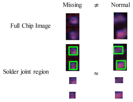
Figure 13.
Failure case in defect classification using a dual-input CNN.
8. Conclusions
In this paper, we proposed a CNN model that combines two solder regions as inputs. We extracted solder regions based on vertical and horizontal projections and then constructed a CNN model. Through defect classification experiments, we confirmed that this late-merge dual-stream CNN has a higher performance and lower weight than can be obtained by conventional methods. The proposed method improved the F1-score by 5.3% compared to single-stream CNN and reduced the weight by about 4000 KB. In addition, the inference time of the proposed method was slightly faster, about 0.3 ms, compared to a single-stream CNN. However, the proposed method requires an accurate solder region extraction. In addition, due to the loss of low-level features, the classification performance of defects was inferior to that of a single-stream CNN for some defects such as missing defects.
Notable advantages and disadvantages of our paper can be summarized as follows.
Advantages:
- The proposed method achieves a higher accuracy and F1-score than single-stream CNN based on a full chip component image.
- The weight of the model is less than for single-stream CNN.
- The proposed method has a faster inference speed than single-stream CNN.
Disadvantages:
- The proposed method requires accurate solder region detection.
- The classification accuracy of single-stream CNN is higher for some defects.
In the future, it would be useful to study both partial and full images, as defect classification performance can be increased by using features extracted from these images. In addition, it is likely possible to reduce the inference time of the proposed method by using only the feature region in which the defect appears as the input of the CNN.
Author Contributions
Conceptualization, Y.-G.K., and T.-H.P.; methodology, Y.-G.K.; project administration, T.-H.P.; All authors have read and agreed to the published version of the manuscript.
Funding
This research was supported by the MSIT (Ministry of Science and ICT), Korea, under the Grand Information Technology Research Center support program (IITP-2020-0-01462) supervised by the IITP (Institute for Information & communications Technology Planning & Evaluation)
Conflicts of Interest
The authors declare no conflict of interest.
Appendix A
Figure A1 shows the confusion matrix of single-stream and dual-stream CNN and Table A1, Table A2 and Table A3 show the true positive (TP), false positive (FP), and false negative (FN) of the classification results. Single-stream CNN and early-merge dual-stream CNN displayed higher FN and FP ratios for under-solder defects than the proposed method. Subsequently, the precision and recall are lower than for the proposed method, and it also affects the F1-score. On the other hand, the proposed method has a lower FP and FN for the under-solder. This result indicates that the high-level feature is effective for classifying defects similar to normal. In the early merge, unlike other methods, it can be seen that the classification accuracy of missing defects and Tombstone defects is high, thus confirming that the combination of low-level features is effective for the classification of defects such as missing defect, which is different from normal.

Figure A1.
Confusion matrix for single-stream CNN (left), early-merge dual-stream CNN (center), late-merge dual-stream CNN (right).
Figure A1.
Confusion matrix for single-stream CNN (left), early-merge dual-stream CNN (center), late-merge dual-stream CNN (right).

Table A1.
Classification results of single-stream CNN.
Table A1.
Classification results of single-stream CNN.
| Measure | TP | FN | FP | |
|---|---|---|---|---|
| Defect | ||||
| Over-Solder | 36 | 0 | 14 | |
| Manhattan | 34 | 1 | 8 | |
| Missing | 559 | 21 | 24 | |
| Normal | 3195 | 68 | 34 | |
| Under-Solder | 192 | 31 | 37 | |
| Tombstone | 168 | 4 | 8 | |
Table A2.
Classification results of early-merge dual-stream CNN.
Table A2.
Classification results of early-merge dual-stream CNN.
| Method | TP | FN | FP | |
|---|---|---|---|---|
| Measure | ||||
| Over-Solder | 33 | 3 | 4 | |
| Manhattan | 33 | 2 | 7 | |
| Missing | 580 | 0 | 29 | |
| Normal | 3054 | 209 | 70 | |
| Under-Solder | 138 | 85 | 175 | |
| Tombstone | 172 | 0 | 14 | |
Table A3.
Classification results of late-merge dual-stream CNN.
Table A3.
Classification results of late-merge dual-stream CNN.
| Method | TP | FN | FP | |
|---|---|---|---|---|
| Measure | ||||
| Over-Solder | 34 | 2 | 1 | |
| Manhattan | 35 | 0 | 0 | |
| Missing | 513 | 67 | 4 | |
| Normal | 3253 | 10 | 75 | |
| Under-Solder | 210 | 13 | 8 | |
| Tombstone | 171 | 1 | 5 | |
Appendix B
Table A4 shows the experimental results of the proposed method with and without ResBlock applied in a late-merge dual-stream CNN. The CNN without ResBlock is the same as the proposed method, except that the skip connection is removed from ResBlock. Both methods were tested using the same experimental environment as the 7.1 Experimental Set-up. The proposed method with ResBlock showed higher performance in terms of average accuracy, precision, recall, and F1-score by 1.8%, 8.6%, 1.8%, and 5.3%, respectively.
Table A4.
Performance of ResBlock.
Table A4.
Performance of ResBlock.
| Method | Late-Merge Dual-Stream | ||
|---|---|---|---|
| Measure | Without ResBlock | With ResBlock | |
| Average Accuracy (%) | 94.2% | 96.0% | |
| Precision (%) | 89.3% | 97.9% | |
| Recall (%) | 94.2% | 96.0% | |
| F1-score (%) | 91.7% | 97.0% | |
References
- Jing, L.; Jinan, G.; Zedong, H.; Jia, W. Application research of improved yolo v3 algorithm in PCB electronic component detection. Appl. Sci. 2019, 9, 3750. [Google Scholar]
- Yajun, C.; Peng, H.; Min, G.; Erhu, Z. Automatic feature region searching algorithm for image registration in printing defect inspection systems. Appl. Sci. 2019, 9, 4838. [Google Scholar]
- Yuk, E.H.; Park, S.H.; Park, C.S.; Baek, J.G. Feature-learning-based printed circuit board inspection via speeded-up robust features and random forest. Appl. Sci. 2018, 8, 932. [Google Scholar] [CrossRef]
- Xie, H.; Kuang, Y.; Zhang, X. A High Speed AOI Algorithm for Chip Component Based on Image Difference. In Proceedings of the IEEE International Conference on Information Automation, Zhuhai, Macau, China, 22–25 June 2009; pp. 969–974. [Google Scholar]
- Wu, H.; Feng, G.; Li, H.; Zeng, X. Automated Visual Inspection of Surface Mounted Chip Components. In Proceedings of the International Conference on Mechatronics and Automation, Xi’an, China, 4–7 August 2010; pp. 1789–1794. [Google Scholar]
- Wu, F.; Zhang, X. Feature-extraction-based inspection algorithm for IC solder joints. IEEE Trans. Compon. Packag. Manuf. Technol. 2011, 1, 689–694. [Google Scholar]
- Cai, N.; Lin, J.; Ye, Q.; Wang, H.; Weng, S.; Ling, B.W.K. Automatic optical inspection system based on an improved visual background extraction algorithm. IEEE Trans. Compon. Packag. Manuf. Technol. 2016, 6, 161–172. [Google Scholar]
- Ye, Q.; Cai, N.; Li, J.; Li, F.; Wang, H.; Chen, X. IC solder joint inspection based on an adaptive-template method. IEEE Trans. Compon. Packag. Manuf. Technol. 2018, 8, 1121–1127. [Google Scholar] [CrossRef]
- Hongwei, X.; Xianmin, Z.; Yongcong, K.; Gaofei, O. Solder joint inspection method for chip component using improved AdaBoost and decision tree. IEEE Trans. Compon. Packag. Manuf. Technol. 2011, 1, 2018–2027. [Google Scholar] [CrossRef]
- Wu, H.; Zhang, X.; Xie, H.; Kuang, Y.; Ouyang, G. Classification of solder joint using feature selection based on Bayes and support vector machine. IEEE Trans. Compon. Packag. Manuf. Technol. 2013, 3, 516–522. [Google Scholar] [CrossRef]
- Wu, H.; Zhang, X.; Kuang, Y.; Ouyang, G.; Xie, H. Solder joint inspection based on neural network combined with genetic algorithm. Optik 2013, 124, 4110–4116. [Google Scholar]
- Wu, F.; Zhang, X. An inspection and classification method for chip solder joints using color grads and Boolean rules. Int. J. Robot. Comput. Integr. Manuf. 2014, 30, 517–526. [Google Scholar] [CrossRef]
- Acciani, G.; Brunetti, G.; Fornarelli, G. A multiple neural network system to classify solder joints on integrated circuits. Int. J. Comput. Intell. Res. 2006, 2, 337–348. [Google Scholar] [CrossRef]
- Acciani, G.; Brunetti, G.; Fornarelli, G. Application of neural networks in optical inspection and classification of solder joints in surface mount technology. IEEE Trans. Ind. Informat. 2006, 2, 200–209. [Google Scholar] [CrossRef]
- Song, J.D.; Kim, Y.G.; Park, T.H. Defect classification method of PCB solder joint by color features and region segmentation. J. Control Robot. Syst. 2017, 23, 1086–1091. [Google Scholar] [CrossRef]
- Song, J.D.; Kim, Y.G.; Park, T.H. SMT Defect classification by feature extraction region optimization and machine learning. Int. J. Adv. Manuf. Technol. 2019, 101, 1303–1313. [Google Scholar] [CrossRef]
- Nakazawa, T.; Kulkarni, D.V. Wafer map defect pattern classification and image retrieval using convolutional neural network. IEEE Trans. Semicond. Manuf. 2018, 31, 116–123. [Google Scholar] [CrossRef]
- Yang, H.; Song, K.; Tao, B.; Yin, Z. Transfer-learning-based online Mura defect classification. IEEE Trans. Semicond. Manuf. 2018, 31, 116–123. [Google Scholar] [CrossRef]
- Cheon, S.J.; Lee, H.K.; Kim, C.O.; Lee, S.H. Convolutional neural network for wafer surface defect classification and the detection of unknown defect class. IEEE Trans. Semicond. Manuf. 2019, 32, 163–170. [Google Scholar] [CrossRef]
- Di, H.; Ke, X.; Peng, Z.; Dongdong, Z. Surface defect classification of steels with a new semi-supervised learning method. Opt. Lasers Eng. 2019, 1777, 40–48. [Google Scholar] [CrossRef]
- Xie, Q.; Li, D.; Xu, J.; Yu, Z.; Wang, J. Automatic detection and classification of sewer defects via hierarchical deep learning. IEEE Trans. Autom. Sci. Eng. 2019, 16, 1836–1847. [Google Scholar] [CrossRef]
- Li, Y.; Zhao, W.; Pan, J. Deformable patterned fabric defect detection with fisher criterion-based deep learning. IEEE Trans. Autom. Sci. Eng. 2017, 14, 1256–1264. [Google Scholar] [CrossRef]
- Yang, H.; Chen, Y.; Song, K.; Yin, Z. Multiscale feature-clustering-based fully convolutional autoencoder for fast accurate visual inspection of texture surface defects. IEEE Trans. Autom. Sci. Eng. 2019, 16, 1450–1467. [Google Scholar] [CrossRef]
- Cai, N.; Cen, G.; Wu, J.; Li, F.; Wang, H.; Chen, X. SMT solder joint inspection via a novel cascaded convolutional neural network. IEEE Trans. Autom. Sci. Eng. 2018, 8, 670–677. [Google Scholar] [CrossRef]
- Kim, Y.G.; Park, T.H. Defect classification of SMD defect based on deep learning. In Proceedings of the Conference on Information and Control Systems, Mokpo, Korea, 26–28 October 2017; pp. 15–16. [Google Scholar]
- Williams, A. Build Your Own Printed Circuit Board, 1st ed.; McGraw-Hill Professional: New York, NY, USA, 2003; p. 121. [Google Scholar]
- Otsu, N. A threshold selection method from gray level histograms. IEEE Trans. Syst. Man Cybern. Syst. 1979, 9, 62–66. [Google Scholar] [CrossRef]
- Krizhevsky, A.; Sutskever, I.; Hinton, G.E. ImageNet Classification with Deep Convolutional Neural Networks. In Proceedings of the International Conference on Neural Information Processing Systems 2012 (NIPS 2012), Lake Tahoe, NV, USA, 3–8 December 2012; pp. 1–9. [Google Scholar]
- Saimonyan, K.; Zisserman, A. Very deep convolutional networks for large-scale image recognition. arXiv 2014, arXiv:1409.1556. [Google Scholar]
- He, K.; Zhang, X.; Ren, S.; Sun, J. Deep Residual Learning for Image Recognition. In Proceedings of the IEEE Conference on Computer Vision and Pattern Recognition 2016, Las vegas, NV, USA, 26 June–1 July 2016; pp. 770–778. [Google Scholar]
- Szegedy, C.; Loffe, S.; Vanhoucke, V.; Alemi, A. Inception-v4, inception-resnet and the impact of residual connections on learning. arXiv 2017, arXiv:1602.07261v2. [Google Scholar]
- Rumelhart, D.; Hinton, G.; Williams, R. Learning representations by back-propagating errors. Nature 1986, 323, 533–536. [Google Scholar] [CrossRef]
- Kingma, D.; Ba, J. Adam: A method for stochastic optimization. arXiv 2014, arXiv:1412.6980v9. [Google Scholar]


© 2020 by the authors. Licensee MDPI, Basel, Switzerland. This article is an open access article distributed under the terms and conditions of the Creative Commons Attribution (CC BY) license (http://creativecommons.org/licenses/by/4.0/).