Article

Numerical Analysis of Midinfrared D-Shaped Photonic-Crystal-Fiber Sensor Based on Surface-Plasmon-Resonance Effect for Environmental Monitoring

1
Key Laboratory of Optical Technology and Instrument for Medicine, Ministry of Education, University of Shanghai for Science and Technology, Shanghai 200093, China
2
Shanghai Institute of Intelligent Science and Technology, Tongji University, Shanghai 200092, China
*
Author to whom correspondence should be addressed.
Appl. Sci. 2020, 10(11), 3897; https://doi.org/10.3390/app10113897
Submission received: 19 May 2020 / Revised: 31 May 2020 / Accepted: 2 June 2020 / Published: 4 June 2020

Abstract

:
An exciting prospect for the sensing community is the potential of midinfrared fiber sensors. Taking advantage of the design flexibility of photonic crystal fiber and the high excitation loss of gold layers, a high-performance midinfrared D-shaped sensor based on the surface-plasmon-resonance effect was designed and numerically investigated by a mature finite-element tool. Numerical results showed that the designed fiber is especially suitable for sensing. In an operating wavelength ranging from 2.9 to 3.6 μm, maximal wavelength sensitivity of 11,500 nm/refractive index unit (RIU) and a maximal refractive index (RI) resolution of 8.7 × 10⁻⁶ RIU were obtained by the wavelength-interrogation method when analyte RI varied from 1.36 to 1.37. Maximal amplitude sensitivity of 230 RIU−1 was obtained by the amplitude-interrogation method with a high linearity of 0.99519 and an adequate figure of merit of 142. Additionally, the sensor had good fabrication tolerance. Our sensor is a promising candidate for environmental monitoring.

1. Introduction

Sensors based on the surface-plasmon-resonance (SPR) effect can be applied in many detection fields because they possess high sensitivity, simple operation, and online detection [1,2,3,4,5]. Different from traditional Kretschmann prism-type SPR sensors, fiber-based sensors are widely acclaimed due to the excellent virtues of micro–nano dimensions, low cost, anti-interference, and ease of remote real-time monitoring [6,7,8]. Generally, there are two main methods to implement fiber SPR sensors. First, in order to produce a sensor with specific performance, we need to process the carrier fiber, and common processing techniques such as bending, taper, engraved grating, and side polishing. Second, in order to stimulate surface plasmons (SPs) for sensors, excitation-metal wire filling, inner and outer coating, and fiber end coating can be selected. Unfortunately, conventional glass-based fibers are not only less flexible in design, which results in limited sensing performance, but also very fragile, which makes conventional fibers unable to be excessively processed [9]. Therefore, it is necessary to find a flexible and easily fabricated scheme.
In view of the lack of design flexibility in conventional fibers, photonic crystal fiber [10,11,12] (PCF), which is known as the catalyst for the fiber industry, is a promising candidate and may become a satisfactory sensing platform. For a PCF-based sensor, more superior sensing characteristics are produced by combining the SPR phenomenon because of its small dimension and flexible design advantages. Depending on the PCF structural parameters used to control light transmission, many optical properties in PCFs, such as nonlinearity, dispersion, effective mode field area, and mode birefringence, can easily be tailored. Accordingly, sensing characteristics can also become rich. In our scheme, side polishing was selected for fiber processing because it greatly simplified the fabrication of the sensor.
In recent years, an increasing number of D-shaped PCF sensors were designed and investigated thanks to the SPR effect. For instance, in 2012, Tian et al. reported a D-shaped SPR sensor based on an all-solid PCF, showing at least 7300 nm/refractive index unit (RIU) for spectral sensitivity, and 216 for figure of merit (FOM) in the visible band [13]. In 2014, Tan et al. designed a side-polished fiber sensor with a gold layer and liquid filling operating from 500 to 750 nm, and sensitivity over 6430 nm/RIU [14]. In 2015, Santos et al. proposed a D-shaped fiber sensor with a coated gold layer operating from 500 to 900 nm that obtained sensitivity of 10 × 103 nm/RIU with a resolution of 9.8 × 10⁻⁶ RIU [15]. In 2016, Dash et al. analyzed a highly sensitive D-shaped sensor. The sensor showed wavelength sensitivity of 5200 nm/RIU and resolution of 1.92 × 10⁻⁵ RIU in the wavelength range of 1600–2100 nm [16]. In 2017, a novel D-shaped sensor based on endless single-mode PCFs and SPR was experimentally demonstrated by Chen et al. that obtained sensitivity of 6.53 × 10⁻⁵ RIU in the visible band [17]. Gangwar et al. proposed a D-shaped PCF–SPR sensor with average sensitivity of 7700 nm/RIU and resolution of 1.30×10⁻⁵ RIU for analyte refractive index (RI) varying between 1.43 and 1.46 [18]. Wu et al. theoretically and experimentally analyzed a D-shaped sensor with maximal sensitivity of 21,700 nm/RIU in the visible band [19]. In 2018, Wu et al. numerically investigated a novel D-shaped sensor. Sensitivity of 31,000 nm/RIU was obtained in the near-infrared band [20]. Chen et al. demonstrated a novel D-shaped PCF–SPR sensor for low RI detection; maximal spectral sensitivity of 11,055 nm/RIU and RI resolution of 9.05 × 10⁻⁶ RIU were obtained in the range from 2.35 to 2.65 μm [21].
Two common characteristics can be found from the designs described above. For sensing performance, modern sensors are moving toward high sensitivity and high resolution. For fabrication, the processing technology of side polishing is easier to operate during the sensor-manufacturing process while achieving excellent performance. Therefore, proposed sensors with both the virtues of high sensitivity and easy manufacturing are very popular. However, we also found that most sensors operate in the visible or near-infrared bands, and sensors working in the midinfrared band are not very common. Usually, molecules can interact with midinfrared light by absorbing or emitting light that allows for the qualitative and quantitative detection of chemicals in environment engineering [22]. Facing increasingly serious environmental problems, the demand for midinfrared sensors for accurate and real-time environmental monitoring is gradually increasing and cost is high, so sensors operating in the midinfrared band show great research value. Focusing on the midinfrared band, we designed a simple D-shaped PCF–SPR sensor and numerically investigated it. Considering the chemical stability and resonance output energy of excitation materials, we selected gold (Au) as the sensing-layer medium. We numerically analyzed the effect of the structural parameters on sensing performance by the finite-element method (FEM) [23], and explored sensing sensitivity to analyte RI changes, linearity, and FOM. Finally, fabrication-tolerance analysis was considered.

2. Model and Theory

The midinfrared D-shaped PCF–SPR sensor’s structure was obtained by side-polishing a three-layer hexagonal-lattice PCF to form a plane that was coated with a gold layer by the sputter-deposition method (SDM) [24]. When the sensor was operating, the gold layer was directly in contact with the analyte to be detected. Figure 1a displays the cross-section illustration of our sensor. The lattice pitch was Λ1 = 6.0μm, the cladding holes’ diameters and two central holes are represented by d1 and d2, respectively, and we first set d1 = 2.8 μm. Other structural parameters, namely, channel length, gold-layer thickness, and analyte RI are characterized by Λ2, TAu, and na, respectively.
The background material of the PCF was Si. Resonance wavelength between Si and the excitation gold layer was located exactly in the midinfrared band. The RI of Si can be characterized by a Sellmeier equation [25] that is described as
n S i ( λ ) = ε + A λ 2 + B λ 1 2 λ 2 λ 1 2
where λ represents a free space wavelength, and detailed parameters were ε = 11.6858, λ1 = 1.1071 μm, A = 0.939816 μm2, and B = 8.10461×10⁻³, respectively.
The dielectric constant of the gold sensing layer in the wavelength region from 0.248 to 6.2 μm can be characterized by the Drude–Lorentz (DL) model [26,27,28]:
ε ( ω ) = ε 1 + i ε 2 = ε ω p 2 ω ( ω + i ω c )
where ω = 2 π / λ , and detailed parameters were ε = 9.75 , ω p = 1.36 × 10 16 , and ω c = 1.45 × 10 14 , respectively.
In the sensor’s performance analysis, we adopted confinement loss (CL) [29,30] to characterize the detection signal. Usually, CL can be expressed by
α = 8.686 × 2 π λ × I m ( n e f f ) × 10 4 ( d B / c m )
where λ represents the incident-light wavelength and I m ( n e f f ) represents the effective RI imaginary part for the core fundamental mode (FM). In order to facilitate understanding the following formulas, α in dB/cm here represents CL.
In our works, sensor performance was examined on the basis of wavelength sensitivity (WS) [31], amplitude sensitivity (AS) [32], RI resolution [33], linearity [34], and FOM [35]. Common wavelength-interrogation method (WIM) and amplitude-interrogation method (AIM) [36] were employed for analyzing these performance parameters.
Usually, WS, AS, and RI resolution are the three most common parameters for measuring sensor performance. WS is described by
S ( λ ) = Δ λ p e a k / Δ n a   ( n m / R I U )
where Δ λ p e a k represents the shift of the resonance wavelength and Δ n a represents RI variations; here, Δ n a is 0.01.
AS is described by
S A ( λ ) = 1 α ( λ , n a ) α ( λ , n a ) n a ( R I U 1 ) ,
where α ( λ , n a ) represents CL when the detected RI was na, and α ( λ , n a ) represents the CL difference when RI variation was n a .
RI resolution is described by
R = Δ n a · Δ λ m i n Δ λ p e a k ( R I U ) ,
where Δ λ m i n is wavelength resolution assuming that Δ λ m i n is 0.1 nm for the purposes of calculation [37,38].
The FOM was adopted for evaluating accuracy of detection in sensors. It is a key factor combining full width at half maximum (FWHM) and signal-to-noise ratio (SNR), which is described by
F O M = m F W H M
where m denotes the slope of two adjacent resonance points, and FWHM denotes the full width at half the maximum peak of each detected signal [39].
For performance analysis, commercial COMSOL 5.2 software integrating an FEM solver was utilized to study transmission and coupling properties in PCFs, combining a perfect match layer (PML) [40]. Here, PML thickness was 5μm. The electromagnetic-mode patterns of the sensor fiber could be achieved quickly and precisely. The cross-section was discretized as depicted in Figure 1b, and divided into 106,026 mesh elements in total for computing. A mobile workstation with an Intel Core i7 CPU and 8 G random access memory (RAM) was also utilized to support software operation.

3. Numerical Results and Discussion

3.1. Mode-Coupling Properties

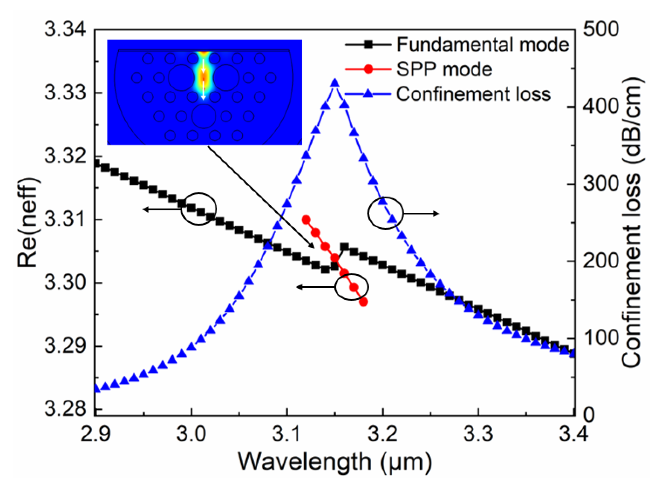
In the proposed sensor, (a) x-polarization core FM, (b) y-polarization core FM, and (c) surface-plasmon-polariton (SPP) mode in the sensing layer were analyzed as shown in Figure 2. The way in which plasmonic mode interacted with the FM through the middle channel (direction of white arrow) was adopted. In the light–matter interaction on the gold–dielectric interface, although x- and y-polarization FMs existed simultaneously in the core, only y-polarization FM could be utilized to excite SPs. According to the dispersion relations of the y-polarization FM and plasmonic mode in Figure 3, there was a detectable loss signal at the intersection of the two RI curves. The inset indicates the resonance state of y-polarization FM and plasmonic mode. As stated in coupled-mode theory (CMT) [41,42], when FM and SPP mode satisfy mode-resonance conditions, the energy carried by the two modes can produce a sufficient exchange. The evanescent field in the fiber could be greatly strengthened, and a sharp loss signal appears. Fortunately, thanks to its uniqueness, only y-polarization FM could resonate with SPP mode in the investigated band. There was only one loss signal at the intersection of the two curves that is very suitable to apply in the sensing field. According to the uniqueness of resonance peak in the sensor, the precise detection of the analyte RI could be achieved.

3.2. Structural-Parameter Determination

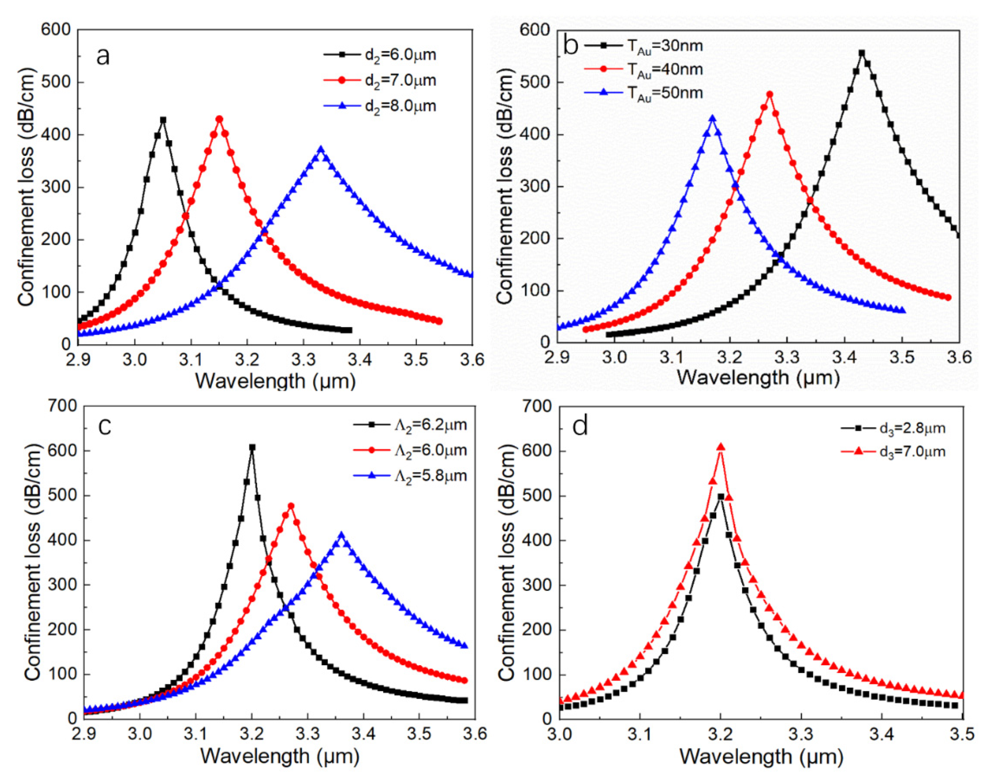
It is well known that the influence of PCF structural parameters is sensitive on sensing characterization. In this section, diameter of central two holes d2, thickness of gold layer TAu, channel length Λ2, and hole diameter d3 were considered for numerical investigation.
Figure 4a depicts loss spectra for different diameters of central holes d2 with d1 = 2.8 μm, d3 = 7.0 μm, Λ1 = Λ2 = 6.0 μm, TAu = 50 nm, and na = 1.36, making d2 6.0, 7.0, and 8.0 μm, respectively. The position of resonance wavelength occurred as a redshift with the increase of d2. Simultaneously, the corresponding resonance signal was also changed; especially in the case of d2 = 8 μm, the signal was reduced and widened because diameter d2 was too large, and the area of the core was reduced, which made it difficult to maintain good single-mode transmission of the PCF, so y-polarization FM could not generate a strong mode-coupling effect with the SPP mode. Thus, we should avoid the value of d2, which was too large in the sensor design. Under conditions of d2 = 6 and 7 μm, the energy produced by the latter was also slightly larger than that of the former in calculation; if more loss energy could be generated, the signal would be easier to detect, so the case of d2 = 7 μm was selected for the next analysis.
Obviously, the role of excitation-gold-layer thickness in sensing is very important. So, the influence of different gold-layer thicknesses TAu on the sensor was considered, as shown in Figure 4b. We observed that, when TAu increased, the CL peak was blue-shifted, and the loss peak was reduced. The reason for this phenomenon was the thinner thickness of the gold layer; the more obvious the effect of light–matter interaction, the more that free oscillation was enhanced. This process also enhanced the evanescent field near the dielectric interface, which distinctly led to strong energy generation that would be weaker. However, in the course of use, the gold layer would certainly be consumed and it could not be designed to be very thin in a one-sided pursuit of high-loss signals. So, TAu = 40 nm was selected as a compromise between gold-layer thickness and signal strength.
Figure 4c displays loss spectra for different channel lengths Λ2 with d1 = 2.8 μm, d2 = d3 = 7.0 μm, Λ1 = 6.0 μm, TAu = 40 nm, and na = 1.36. The Λ2 variation also induced the changes of resonance wavelength and loss peak. It was obvious that, with the increase of Λ2, the loss peak shifted towards the shorter wavelength direction, and signal peak increased. The cause of this phenomenon was that, as Λ2 is increased, light in the core region penetrated more into the cladding, and the evanescent field increased, so the CL increased.
Figure 4d displays loss spectra for different d3 with d1 = 2.8 μm, d2 = 7.0 μm, Λ1 = 6, Λ2 = 6.2 μm, TAu = 40 nm, and na = 1.36. When d3 was 2.8 μm, the surrounding medium of the d3 hole had a binding effect on the light, and the light travelling in the PCF core dissipated to a certain extent. Therefore, it was necessary to design d3 to be 7.0 μm. On the one hand, when d3 = 7.0 μm, the energy was significantly improved to facilitate signal detection. On the other hand, the same size as d2 reduced fabrication complexity.
On the basis of the above phenomenon, in the investigated band ranging from 2.9 to 3.6 μm, we selected the parameters of d1 = 2.8 μm, d2 = d3 = 7.0 μm, Λ1 = 6.0 μm, Λ2 = 6.2 μm, and TAu = 40 nm for the next performance discussion.

3.3. Sensor-Performance Investigations

It was clearly found that the proposed D-shaped sensor’s performance relied on the resonance wavelength moving, induced by changing the detected analyte RI, which might have been caused by environment variations surrounding the sensing layer. According to Section 3.1, due to the uniform distribution of the loss spectra and the single peak in the investigated band, it was very suitable for sensing applications.
Figure 5a describes loss spectra for different analyte RIs between 1.33 and 1.39 with d1 = 2.8 μm, d2 = d3 = 7.0 μm, Λ1 = 6.0 μm, Λ2 = 6.2 μm, and TAu = 40 nm. By the WIM, when the RI varied from 1.33 to 1.39, the corresponding resonance wavelength could be tuned from 2.9 to 3.6 μm. Results showed that the average Δ λ p e a k was about 88.5 nm; hence, average WS was 8850 nm/RIU and RI resolution was 1.13 × 10⁻⁵ RIU in this sensor. Maximal WS emerged when the analyte RI varied from 1.36 to 1.37. The maximal value could reach 11,500 nm/RIU, and the corresponding RI resolution was 8.7 × 10⁻⁶ RIU. Figure 5b describes amplitude sensitivity with different analyte RIs by the AIM. We found that the AS peak decreased as RI changed from 1.33 to 1.39, and maximal AS was 230 RIU−1 when na was 1.33.
Next, the linearity of the sensor was analyzed. Figure 5c shows that resonance points were distributed on both sides of the red solid line. This indicated an approximately linear relationship between analyte RIs and resonance wavelengths. By calculation, the fitting equation for this sensor was expressed as follows:
λ o = 8.67143 n a 8.57857 ,   ( 1.33 n a 1.39 )
where na and λ o denote analyte RI and operating wavelength, respectively. The adjusted R2 was a powerful tool to help us judge linearity [43]. According to these resonance points, an adjusted R2 of 0.99519 was obtained that verified a highly linear correlation degree between na and λ o .
Figure 5d shows the FOM of our sensor versus different analyte RIs. As the analyte RI varied between 1.33 and 1.39, FOM first increased and then decreased; it was obvious that, when na = 1.37, an adequate FOM of 142 could be achieved.
For comparison, Table 1 displays the major performance parameters of our sensor and some existing D-shaped sensors. We found that the maximal WS, RI resolution, linearity, and FOM of our D-shaped sensor could then reach the highest order of magnitude, but sensors simultaneously with these characteristics are uncommon. Among existing midinfrared sensors, for example, Liu et al. proposed a dual open-ring structured sensor with average WS of 5500 nm/RIU, AS of 333.8 RIU−1, and maximal resolution of 7.69 × 10⁻⁶ RIU [44]. Chen et al. obtained a D-shaped sensor with maximal WS of 11055 nm/RIU and RI resolution of 9.05 × 10⁻⁶ [21], but they did not consider linearity and FOM. In comparison, our sensor combined four excellent performance advantages and possesses broad prospects for various midinfrared applications.

4. Structural-Tolerance Discussion

It is actually difficult to ensure the accurate control of structural parameters in PCFs because the difference in temperature control causes air holes to produce different degrees of shrinkage and slight changes in the lattice pitch in cladding during the fabrication process. Hence, although the proposed sensor could be completely manufactured by stack-and-draw technology [48,49], side polishing [50], and SDM, PCF fabrication tolerance still needs to be discussed.
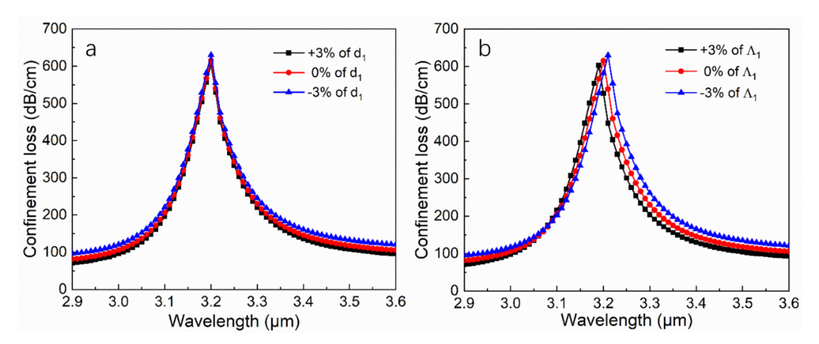
Usually, about ±1% variation in PCF structure parameters is inevitable. We investigated the effect on the variation of d1 of ±3% and that of Λ1 of ±3% to briefly consider the possibility of PCF fabrication. The case of d1 = 2.8 μm, d2 = d3 = 7.0 μm, Λ1 = 6.0μm, Λ2 = 6.2 μm, and TAu = 40 nm was considered. Figure 6a shows that ±3% variation brought about a small shift in resonance wavelength and a slight floating of energy. The effect was almost negligible. Figure 6b shows the loss spectra for Λ1 variation of ±3 %, where we found the effect of Λ1 on resonance-wavelength shift and energy change was more pronounced than that of d1, but the overall effect was limited. The accelerated development of this technology could tailor these changes to be negligible. In this sensor, for slight variations in the PCF structure, the loss-signal change of the sensor was still small, which indicated high fabrication tolerance.

5. Conclusions

In summary, this paper numerically analyzed the sensing characteristics of a high-performance midinfrared D-shaped PCF–SPR RI sensor. An FEM tool was employed to investigate sensing performance. The influence of the structural parameters, and the relationship between resonance wavelengths and analyte RI (1.33–1.39) were discussed for the sensor. Simulation results showed that the effect of central-hole diameter d2, gold-layer thickness TAu, channel length Λ2, and hole diameter d3 was sensitive on the sensor. Using the WIM, average WS of 8850 nm/RIU and an average RI resolution of 1.13 × 10⁻⁵ RIU were achieved; maximal WS and maximal RI resolution were 11,500 nm/RIU and 8.7 × 10⁻⁶ RIU, respectively, when the analyte RI changed between 1.36 and 1.37. Using the AIM, maximal AS of 230 could be achieved. The sensor simultaneously had high linearity with the adjusted R2 of 0.99519 and an adequate FOM of 142. In addition, the sensor had good fabrication tolerance. So, we have no reason to doubt that our sensor could be applied as a photonic integrated component for real-time environmental monitoring.
In future work, we intend to build an experiment setup to verify the simulated results. For simplicity, a basic midinfrared system comprises a supercontinuous light source covering wavelengths from 2.9 to 3.6 μm, RI selection device, and midinfrared optical-spectrum analyzer (OSA). First, we aim to fuse a single-mode fiber at both ends of the sensor. Second, we will connect the light source, fiber, and OSA in sequence. Third, we will place the sensing section in the RI selection device, and then turn on the light source. Lastly, the corresponding spectrum could be obtained in the OSA by changing the RI.

Author Contributions

Conceptualization, N.C. and M.C.; methodology, N.C.; software, N.C.; validation, N.C., X.L. and M.C.; formal analysis, X.L.; investigation, J.Z.; resources, X.Z.; data curation, M.C.; writing—original draft preparation, N.C.; writing—review and editing, M.C.; visualization, J.Z. and N.C.; supervision, X.Z.; project administration, X.Z.; funding acquisition, X.Z. All authors have read and agreed to the published version of the manuscript.

Funding

This work was financially supported by the National Key Scientific Apparatus Development of Special Item of China (project number 2016YFF0101400).

Acknowledgments

Sincerely thanks Rongfu Zhang, Hui Chen and Junying Li in Shanghai University of Science and technology, for their kindly discussion with authors.

Conflicts of Interest

The authors declare no conflict of interest.

References

  1. Hu, D.J.J.; Ho, H.P. Recent advances in plasmonic photonic crystal fibers: Design, fabrication and applications. Adv. Opt. Photonics 2017, 9, 257–314. [Google Scholar] [CrossRef]
  2. Li, P.; Zhao, J. Polarization-dependent coupling in gold-filled dual-core photonic crystal fibers. Opt. Express 2013, 21, 5232–5238. [Google Scholar] [CrossRef] [PubMed]
  3. Nagasaki, A.; Saitoh, K.; Koshiba, M. Polarization characteristics of photonic crystal fibers selectively filled with metal wires into cladding air holes. Opt. Express 2011, 19, 3799–3808. [Google Scholar] [CrossRef] [PubMed]
  4. Zhang, S.; Yu, X.; Zhang, Y.; Shum, P.; Zhang, Y.; Xia, L.; Liu, D. Theoretical Study of Dual-Core Photonic Crystal Fibers with Metal Wire. IEEE Photonics J. 2012, 4, 1178–1187. [Google Scholar] [CrossRef]
  5. Sazio, P.J.; Amezcuacorrea, A.; Finlayson, C.E.; Hayes, J.R.; Scheidemantel, T.J.; Brail, N.F.; Jackson, B.R.; Won, D.; Zhang, F.; Margine, E.R.; et al. Microstructured optical fibers as high-pressure microfluidic reactors. Science 2006, 311, 1583–1586. [Google Scholar] [CrossRef] [Green Version]
  6. Sharma, A.K.; Gupta, B.D. Fibre-optic sensor based on surface plasmon resonance with Ag-Au alloy nanoparticle films. Nanotechnology 2005, 17, 124. [Google Scholar] [CrossRef]
  7. Jha, R.; Badenes, G. Effect of fiber core dopant concentration on the performance of surface plasmon resonance-based fiber optic sensor. Sensor Actuat. A Phys. 2009, 150, 212–217. [Google Scholar] [CrossRef]
  8. Farahani, M.A.; Gogolla, T. Spontaneous Raman scattering in optical fibers with modulated probe light for distributed temperature Raman remote sensing. J. Lightwave Technol. 1999, 17, 1379. [Google Scholar] [CrossRef]
  9. Tan, Z.; Hao, X.; Shao, Y.; Chen, Y.; Li, X.; Fan, P. Phase modulation and structural effects in a D-shaped all-solid photonic crystal fiber surface plasmon resonance sensor. Opt. Express 2014, 22, 15049–15063. [Google Scholar] [CrossRef]
  10. Knight, J.C. Photonic Crystal Fibers and Fiber Lasers (Invited). J. Opt. Soc. Am. B 2007, 24, 1661–1668. [Google Scholar] [CrossRef]
  11. Russell, P.W. Photonic crystal fibers. Science 2003, 299, 358–362. [Google Scholar] [CrossRef] [PubMed]
  12. Russell, P. Photonic Crystal Fibers. J. Lightwave Technol. 2006, 24, 4729–4749. [Google Scholar] [CrossRef]
  13. Tian, M.; Lu, P.; Chen, L.; Lv, C.; Liu, D. All-solid D-shaped photonic fiber sensor based on surface plasmon resonance. Opt. Commun. 2012, 285, 1550–1554. [Google Scholar] [CrossRef]
  14. Tan, Z.; Li, X.; Chen, Y.; Fan, P. Improving the Sensitivity of Fiber Surface Plasmon Resonance Sensor by Filling Liquid in a Hollow Core Photonic Crystal Fiber. Plasmonics 2014, 9, 167–173. [Google Scholar] [CrossRef] [Green Version]
  15. Santos, D.F.; Guerreiro, A.; Baptista, J.M. SPR Microstructured D-Type Optical Fiber Sensor Configuration for Refractive Index Measurement. IEEE Sens. J. 2015, 15, 5472–5477. [Google Scholar] [CrossRef]
  16. Dash, J.N.; Jha, R. Highly sensitive D shaped PCF sensor based on SPR for near IR. Opt. Quantum Electron. 2016, 48, 137. [Google Scholar] [CrossRef]
  17. Chen, Y.; Xie, Q.; Li, X.; Zhou, H.; Hong, X.; Geng, Y. Experimental realization of D-shaped photonic crystal fiber SPR sensor. J. Appl. Phys. 2017, 50, 025101. [Google Scholar] [CrossRef]
  18. Gangwar, R.K.; Singh, V.K. Highly Sensitive Surface Plasmon Resonance Based D-Shaped Photonic Crystal Fiber Refractive Index Sensor. Plasmonics 2017, 12, 1367–1372. [Google Scholar] [CrossRef]
  19. Wu, T.; Shao, Y.; Wang, Y.; Cao, S.; Cao, W.; Zhang, F.; Liao, C.; He, J.; Huang, Y.; Hou, M.; et al. Surface plasmon resonance biosensor based on gold-coated side-polished hexagonal structure photonic crystal fiber. Opt. Express 2017, 25, 20313–20322. [Google Scholar] [CrossRef] [Green Version]
  20. Wu, J.; Li, S.; Wang, X.; Shi, M.; Feng, X.; Liu, Y. Ultrahigh sensitivity refractive index sensor of a D-shaped PCF based on surface plasmon resonance. Appl. Opt. 2018, 57, 4002–4007. [Google Scholar] [CrossRef]
  21. Chen, X.; Xia, L.; Li, C. Surface Plasmon Resonance Sensor Based on a Novel D-Shaped Photonic Crystal Fiber for Low Refractive Index Detection. IEEE Photonics J. 2018, 10, 1–9. [Google Scholar] [CrossRef]
  22. Schadle, T.; Mizaikoff, B. Mid-Infrared Waveguides: A Perspective. Appl. Spectrosc. 2016, 70, 1625–1638. [Google Scholar] [CrossRef] [PubMed] [Green Version]
  23. Saitoh, K.; Koshiba, M. Numerical Modeling of Photonic Crystal Fibers. J. Lightwave Technol. 2005, 23, 3580–3590. [Google Scholar] [CrossRef] [Green Version]
  24. Lo, Y.L.; Chuang, C.H.; Lin, Z.W. Ultra-high sensitivity polarimetric strain sensor based upon D-shaped optical fiber and surface plasmon resonance technology. Opt. Lett. 2011, 36, 2489–2491. [Google Scholar] [CrossRef]
  25. Osgood, R.M.; Panoiu, N.C.; Dadap, J.I.; Liu, X.; Chen, X.; Hsieh, I.; Dulkeith, E.; Green, W.M.J.; Vlasov, Y.A. Engineering nonlinearities in nanoscale optical systems: Physics and applications in dispersion-engineered silicon nanophotonic wires. Adv. Opt. Photonics 2009, 1, 162–235. [Google Scholar] [CrossRef]
  26. Rakic, A.D.; Djurisicm, A.B.; Elazar, J.; Majewski, M.L. Optical properties of metallic films for vertical-cavity optoelectronic devices. Appl. Opt. 1998, 37, 5271–5283. [Google Scholar] [CrossRef]
  27. Uebel, P.; Schmidt, M.A.; Lee, H.W.; Russell, P.S.J. Polarisation-resolved near-field mapping of a coupled gold nanowire array. Opt. Express 2012, 20, 28409–28417. [Google Scholar] [CrossRef]
  28. Chen, N.; Chang, M.; Lu, X.; Zhou, J.; Zhang, X. Photonic Crystal Fiber Plasmonic Sensor Based on Dual Optofluidic Channel. Sensors. 2019, 19, 5150. [Google Scholar] [CrossRef] [Green Version]
  29. Rifat, A.A.; Mahdiraji, G.A.; Sua, Y.M.; Shee, Y.G.; Ahmed, R.; Chow, D.M.; Adikan, F.R. Surface Plasmon Resonance Photonic Crystal Fiber Biosensor: A Practical Sensing Approach. IEEE Photonic Technol. Lett. 2015, 27, 1628–1631. [Google Scholar] [CrossRef]
  30. Rifat, A.A.; Mahdiraji, G.A.; Shee, Y.G.; Shawon, M.J.; Adikan, F.R.M. A Novel Photonic Crystal FiberBiosensor Using Surface Plasmon Resonance. Procedia Eng. 2016, 140, 1–7. [Google Scholar] [CrossRef] [Green Version]
  31. Hasan, M.R.; Akter, S.; Rifat, A.A.; Rana, S.; Ahmed, K.; Ahmed, K.; Subbaraman, H.; Abbott, D. Spiral Photonic Crystal Fiber-Based Dual-Polarized Surface Plasmon Resonance Biosensor. IEEE Sens. J. 2017, 18, 133–140. [Google Scholar] [CrossRef]
  32. Otupiri, R.; Akowuah, E.K.; Haxha, S.; Ademgil, H.; Abdelmalek, F.; Aggoun, A. A Novel Birefrigent Photonic Crystal Fiber Surface Plasmon Resonance Biosensor. IEEE Photonics J. 2014, 6, 1–11. [Google Scholar] [CrossRef]
  33. Luan, N.; Wang, R.; Lv, W.; Yao, J. Surface plasmon resonance sensor based on D-shaped microstructured optical fiber with hollow core. Opt. Express 2015, 23, 8576–8582. [Google Scholar] [CrossRef] [PubMed]
  34. Chen, N.; Zhang, X.; Nie, F.; Lu, X.; Chang, M. Dispersion-compensating photonic crystal fiber with wavelength tunability based on a modified dual concentric core structure. J. Mod. Opt. 2018, 65, 1459–1465. [Google Scholar] [CrossRef]
  35. Zhu, Z.; Liu, L.; Liu, Z.; Zhang, Y.; Zhang, Y. Surface-plasmon-resonance-based optical-fiber temperature sensor with high sensitivity and high figure of merit. Opt. Lett. 2017, 42, 2948–2951. [Google Scholar] [CrossRef]
  36. Rifat, A.A.; Haider, F.; Ahmed, R.; Mahdiraji, A.; Adikan, F.R.M.; Miroshnichenko, A.E. Highly sensitive selectively coated photonic crystal fiber-based plasmonic sensor. Opt. Lett. 2018, 43, 891–894. [Google Scholar] [CrossRef]
  37. Peng, L.; Shi, F.; Zhou, G.; Ge, S.; Hou, Z.; Xia, C. A Surface Plasmon Biosensor Based on a D-Shaped Microstructured Optical Fiber with Rectangular Lattice. IEEE Photonics J 2015, 7, 1–9. [Google Scholar] [CrossRef]
  38. Paul, A.K.; Sarkar, A.K.; Rahman, A.B.; Khaleque, A. Twin Core Photonic Crystal Fiber Plasmonic Refractive Index Sensor. IEEE Sens. J. 2018, 18, 5761–5769. [Google Scholar] [CrossRef]
  39. Chen, N.; Chang, M.; Zhang, X.; Zhou, J.; Lu, X.; Zhuang, S. Highly Sensitive Plasmonic Sensor Based on a Dual-Side Polished Photonic Crystal Fiber for Component Content Sensing Applications. Nanomaterials 2019, 9, 1587. [Google Scholar] [CrossRef] [Green Version]
  40. Saitoh, K.; Koshiba, M.; Hasegawa, T.; Sasaoka, E. Chromatic dispersion control in photonic crystal fibers: Application to ultra-flattened dispersion. Opt. Express 2003, 11, 843–852. [Google Scholar] [CrossRef]
  41. Shuai, B.; Xia, L.; Liu, D. Coexistence of positive and negative refractive index sensitivity in the liquid-core photonic crystal fiber based plasmonic sensor. Opt. Express 2012, 20, 25858–25866. [Google Scholar] [CrossRef] [PubMed]
  42. Snyder, A.W. Coupled-Mode Theory for Optical Fibers. J. Opt. Soc. Am. 1972, 62, 1267–1277. [Google Scholar] [CrossRef]
  43. Shuai, B.; Xia, L.; Zhang, Y.; Liu, D. A multi-core holey fiber based plasmonic sensor with large detection range and high linearity. Opt. Express 2012, 20, 5974–5986. [Google Scholar] [CrossRef] [PubMed]
  44. Liu, C.; Yang, L.; Lu, X.; Liu, Q.; Wang, F.; Lv, J.; Sun, T.; Mu, H.; Chu, P.K. Mid-infrared surface plasmon resonance sensor based on photonic crystal fibers. Opt. Express 2017, 25, 14227–14237. [Google Scholar] [CrossRef] [PubMed]
  45. Liu, C.; Su, W.; Liu, Q.; Lu, X.; Wang, F.; Sun, T.; Chu, P.K. Symmetrical dual D-shape photonic crystal fibers for surface plasmon resonance sensing. Opt. Express 2018, 26, 9039–9049. [Google Scholar] [CrossRef] [PubMed]
  46. Ramya, K.C.; Kumar, K.V.; Geetha, K.; Boopathi, C.S. Design of D shaped plasmon-photonic crystal fiber for bio sensing application. Results Phys. 2018, 10, 993–994. [Google Scholar] [CrossRef]
  47. Lu, J.; Li, Y.; Han, Y.; Liu, Y.; Gao, J. D-shaped photonic crystal fiber plasmonic refractive index sensor based on gold grating. Appl. Opt. 2018, 57, 5268–5272. [Google Scholar] [CrossRef] [Green Version]
  48. Katagiri, T.; Matsuura, Y.; Miyagi, M. Photonic Bandgap Fiber with a Silica Core and Multilayer Dielectric Cladding. Opt. Lett. 2004, 29, 557–559. [Google Scholar] [CrossRef]
  49. Fitt, A.D.; Furusawa, K.; Monro, T.M.; Please, C.P. Modeling the fabrication of hollow fibers: Capillary drawing. J. Lightwave Technol. 2001, 19, 1924–1931. [Google Scholar] [CrossRef]
  50. Kim, H.; Kim, J.; Paek, U.; Lee, B.H.; Kim, K.T. Tunable photonic crystal fiber coupler based on a side-polishing technique. Opt. Lett. 2004, 29, 1194–1196. [Google Scholar] [CrossRef]
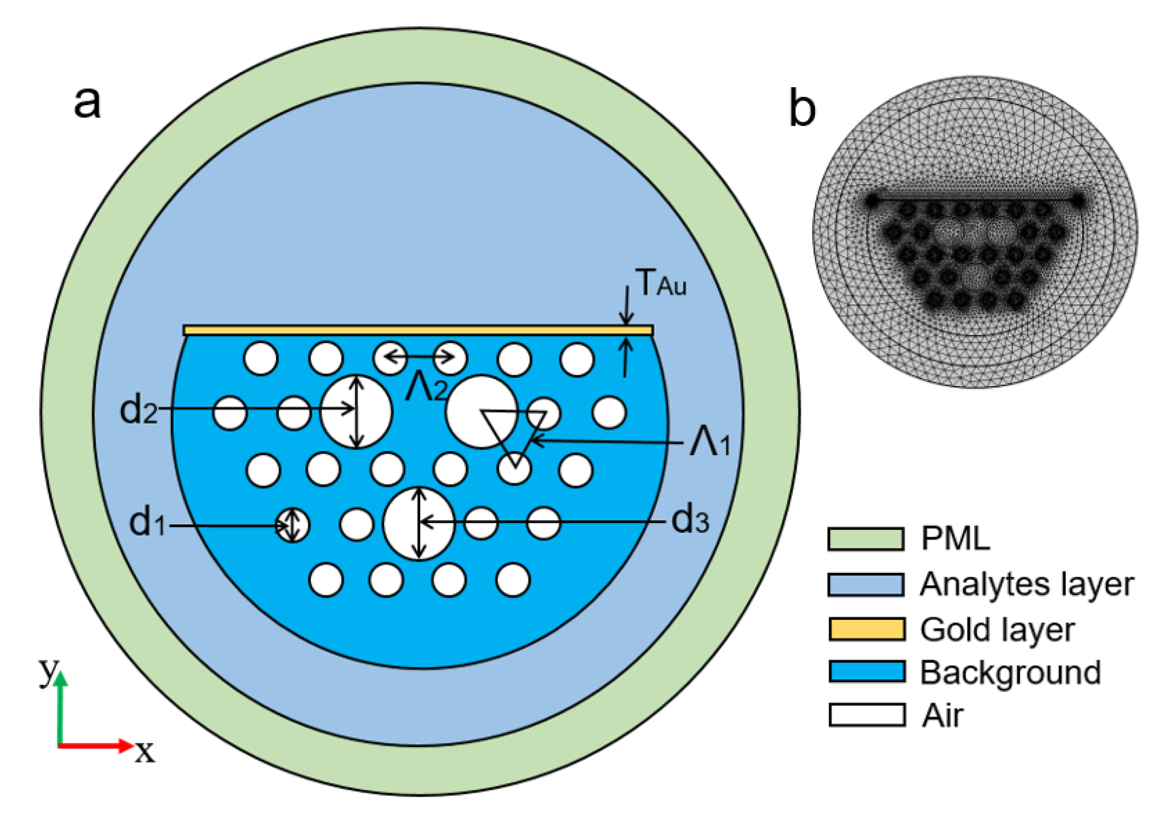
Figure 1. (a) Schematic illustration of designed sensor and (b) finite-element-method (FEM) discretized mesh.
Applsci 10 03897 g001
Figure 2. Mode patterns of fundamental modes (FMs) and plasmonic mode: (a) x-polarization core FM; (b) y-polarization core FM; (c) surface-plasmon-polariton (SPP) mode in sensing layer.
Applsci 10 03897 g002
Figure 3. Dispersion relations of y-polarization core FM and SPP mode in this sensor. Illustration of resonance mode displayed when d1 = 2.8 μm, d2 = d3 = 7.0 μm, Λ1 = Λ2 = 6.0 μm, TAu = 50 nm, and na = 1.36.
Applsci 10 03897 g003
Figure 4. Loss spectra for (a) different diameters of central holes d2 with d1 = 2.8 μm, d3 = 7.0 μm, Λ1 = Λ2 = 6.0 μm, TAu = 50 nm, and na = 1.36; (b) thickness of gold layer TAu with d1 = 2.8 μm, d2 = d3 = 7.0 μm, Λ1 = Λ2 = 6.0 μm, and na = 1.36; (c) different channel lengths Λ2 with d1 = 2.8 μm, d2 = d3 = 7.0 μm, Λ1 = 6.0 μm, TAu = 40 nm, and na = 1.36; (d) different d3 with d1 = 2.8 μm, d2 = 7.0 μm, Λ1 = 6, Λ2 = 6.2 μm, TAu =40 nm, and na = 1.36.
Applsci 10 03897 g004
Figure 5. (a) Loss spectra for different analyte RI na between 1.33 and 1.39; (b) amplitude sensitivity (AS) with different analyte RIs when d1 = 2.8 μm, d2 = d3 = 7.0 μm, Λ1 = 6.0 μm, Λ2 = 6.2 μm, and TAu = 40 nm; (c) linear correlation degree for resonance wavelength versus different analyte RIs; (d) figure of merit (FOM) of this sensor versus different analyte RIs.
Applsci 10 03897 g005
Figure 6. Loss spectra on variation of (a) cladding-hole diameter d1 of ±3% and (b) pitch Λ1 of ±3%.
Applsci 10 03897 g006
Table 1. Comparison results between our sensor and peer D-shaped sensors.
Ref.Max. Wav.
Sens. (nm/RIU)
Max. Resolution
(RIU)
Max. Amp.
Sens. (RIU−1)
LinearityFOM
[13]73001.37 × 10−5N/AN/A216
[15]10,0009.8 × 10−6N/AN/AN/A
[17]2336.26.53 × 10−5N/AN/AN/A
[18]77001.30 × 10−5N/AN/AN/A
[19]21,7004.61 × 10−6N/AN/AN/A
[20]31,0003.23 × 10−6N/AN/AN/A
[21]11,0559.05 × 10−6N/AN/AN/A
[39]12,4009.39 × 10−62520.99692332
[45]14,6606.82 × 10−61222N/A260
[46]70001.43 × 10−5N/AN/AN/A
[47]33405.98 × 10−669.3N/AN/A
This paper11,5008.7 × 10−62300.99519142