Article

The Development of a Modified Design Chain Operations Reference Model in New Product Development of the Printed Circuit Board: A Case Study

1
Department of Industrial and Systems Engineering, Chung Yuan Christian University, Taoyuan City 320, Taiwan
2
Division of Engineering Technology, Wayne State University, Detroit, MI 48202, USA
3
Business School, Minnan Normal University, Zhangzhou 363000, China
4
Analysis and Application of Business Big Data in Key Laboratory of Universities in Fujian Province, No. 36, Qian Zhi Street, Xiangcheng District, Zhangzhou 363000, China
*
Author to whom correspondence should be addressed.
Appl. Sci. 2020, 10(11), 3703; https://doi.org/10.3390/app10113703
Submission received: 21 March 2020 / Revised: 4 May 2020 / Accepted: 20 May 2020 / Published: 27 May 2020
(This article belongs to the Section Applied Industrial Technologies)

Abstract

:
New product development (NPD) is a process of interactions among multiple parties. With stronger competition in the electronic product market, reducing NPD cycle time has become a common important subject in the information technology (IT) industry. The main topic of this research is process improvements in the research and development (R&D) department of the case company by studying how product competitiveness can be enhanced in the current rapid proceeding technology industry. The process-oriented and hierarchical structure is used to analyze the processes of a new printed circuit board (PCB) design and test, and then a modified design chain operations reference (DCOR) model is introduced to explore problems and suggest corresponding solutions. This research also specifies a clear design chain structure for the case firm and improves its R&D process by brainstorming. The goal is to increase the case firm’s PCB design chain efficiency by shortening the delivery time and reducing the problems of risks arising during the NPD. Finally, this research reviews the essence of the design chain management, draws conclusions, and points out directions for future research.

1. Introduction

In an environment of rapid technological innovation, enterprises not only preserve and develop their own core technology, but also utilize a mode of collaboration with external firms by interchanging and applying one another’s professions to obtain more resources and complete the core values [1,2]. The major competitiveness of an enterprise from the collaborative mode of outsourcing leads to winning more ordering opportunities than the competitors by providing an extremely short delivery time and extraordinary product design quality. In such circumstances, one of the key factors of competitiveness is that a new product has a complete research and development (R&D) process, a short R&D time, and outstanding quality to defeat its rivals.
New product development (NPD) is a highly interactive and cooperative process requiring additional attention from not only the R&D department of the enterprise [3,4,5,6,7], but also downstream printed circuit board (PCB) design firms and manufacturers [8,9,10]. If a customer requests an even shorter complete NPD and manufacturing time, it requires collaboration among the customers and the participating firms at every step. Ganotakis et al. [11] stated that the so-called product R&D is a collaboration among the internal units of the enterprise and the external partners to achieve the best efficiency, the shortest delivery time, and the lowest cost. It is a must for an enterprise to construct a complete R&D process for integrating the design chain processes of its internal departments and external companies [12,13].
Many enterprises have their own R&D processes; however, these processes might not be complete with standard protocol, and most of them are just based on the employees’ experiences. It results in not only increasing the risks of failure and the communication time during the product R&D, but also unstable or even decreasing R&D qualities for the new products because of the lack of R&D standards [14]. Therefore, this research builds a set of standard R&D processes that are expected to solve the aforementioned problems of enterprises efficiently so that they can apply the studied complete set of standard R&D processes to improve the competitiveness by shortening the delivery time and reducing the R&D time of new products.
Starting from standardizing the R&D process and using the design chain operations reference (DCOR) model proposed by the Supply Chain Council (SCC) in 2009 as the fundamental theorem [15], this research examines and analyzes the design chain process of NPD and evaluates the feasibility of product R&D for an enterprise. In addition, this research introduces the DCOR model to the case firm’s design process of the new PCB R&D. Through the introduction of the DCOR model, it shortens the delivery time by detecting and refining the shortcomings in the new PCB R&D process.

2. Literature Review

2.1. NPD Process

NPD is one of the conditions for an enterprise to grow and is an important step, including conception, design, customization, and commercialization; therefore, constructing NPD processes is critical. On the other hand, there are alternative definitions of a new product, even when a new factor is added to an existing product. Booz et al. [16] classified products into six categories conforming to companies and the market: new-to-the-world productions, new product line, addition to an existing line, improvements in revision to an existing product, repositioning, and cost reductions. Ullman and David [17] grouped six different steps for the design process: specification R&D/planning, conceptual design, product design, production, service, and product retirement. Cooper [18] proposed a classification of the NPD process: idea, preliminary assessment, concept, R&D, testing, trial, and launch. Baxter and Mike [19] introduced a novel NPD process viewed by designers and classified this process into six items: business opportunity, design specification, concept design, specific design, detail design, and production design. Pahl et al. [20] instead categorized this process into four groups—namely, goal explanation, concept generator, specific design, and detail design—in order to turn the design process into a cycling and improving procedure. During the NPD processes, Lee et al. [21] stated that making a complete design process and an operational protocol of each step is so critical that they can assist in monitoring the variables during the NPD as well as control the design and product qualities. It is easy to delay the time during an entire NPD process because of the various standpoints and unavoidable disagreements among different parties after numerous discussions and experiments. According to [22,23], the IT industry of Taiwan has diverse products and rapid product life cycles. Such rapid life cycles result in inventions of NPD process. Kumar et al. [24] addressed barriers in green lean six sigma product development from an extensive literature review and from experts’ opinions related to developing a hierarchical model structuring these barriers. Song et al. [4] proposed an integrated framework of an innovation network for NPD based on the literature review, and a case study of new refrigerator development revealed the feasibility and potentials of the overall framework to its broad usage in the industry.
From the aforementioned literature, Shih et al. [25] applied the NPD process to illuminate that various engineering problems and design targets can not only simplify the R&D process, but also explicitly clarify the items in the process, thereby solving the problems of shortening the product R&D time and lowering the product’s costs. Sondergaard and Oehmen [26] provided propositions for how to further develop the suggested model as well as how Western companies could learn from Chinese approaches and globalize their product development activities from the front end of the value chain rather than from the back end. Ying et al. [27] presented an NPD case study of a new automatic dishwasher to illustrate the feasibility and validity of the proposed approach; they further performed sensitivity and comparison analyses. Sastoque et al. [28] proposed a project management methodology to create new advanced manufacturing centers whose activities were focused on Technology Readiness Levels (TRL) 5–7.

2.2. DCOR Model

In 1996, Pittiglio Rabin Todd & McGrath, Inc. (PRTM), Advanced Manufacturing Research, Inc. (AMR), and more than 65 enterprises cofounded the SCC and developed the enterprise supply chain operations reference (SCOR) model [15], which includes DCOR and the customer chain operations reference model (CCOR). For example, MacKerron et al. [29] suggested the performance management framework, which was one of the pillars of the SCOR model, and provided practitioners with step-by-step guidelines for the implementation of performance management in outsourcing projects. Georgise et al. [30] examined how a standardized and widely accepted model, like the SCOR, could be applied despite the different circumstances. Choi et al. [31] argued the framework and relations of DCOR processes are threefold: the design process reference model (DPRM), the service component reference model (SCRM), and the technology and standard reference model (TSRM). The SCRM and TSRM correspond with each other. The SCRM needs to specify the technology standards, and technology standards and service components are associated with and assist each other.
In 2004, the SCC first proposed the concept of the DCOR model, which is a specific model dedicated to the design chain. For the complexity of the conventional design language, the DCOR model constructed a complete design language for the designer to achieve flawless communications and design. The SCC released the DCOR model and published the revised DCOR model version 2.0 in 2009 [15]. The DCOR model is an integrated design language and a design chain model, which can gradually create design elements in a top-down manner and correlate them. Lin et al. [32] presented a multi-agent system (MAS) framework developed on the DCOR model to support cooperation between the original design manufacturer (ODM) company and its suppliers. Zuñiga et al. [33] found that DCOR and SCOR models could be extended to model the sourcing process and demonstrated the possibility to extend the SCOR model to the rest of the early supply chain processes of the mineral raw material industry. Ahoa et al. [34] adapted the SCOR model to demonstrate an approach to supporting the configuration of supply chain business processes for dedicated supply chains. The approach was also applied to define and model the Level 4 processes that were beyond the scope of the SCOR model, and scarce relevant literature has been published in many sectors.
In short, the DCOR model is a specified model defined for design chains regulated by the SCC. Currently, the SCC is confined to only Level 1 through Level 3 of the DCOR model. Level 4 of the DCOR model is constructed by enterprises when they introduce their design processes or extend the processes’ items that caught their attention. Because the DCOR model is a gradually developed and analyzed framework, during the analysis, it is suitable to deduct and diagnose the problem points of a design chain process. The enterprise then achieves the improvement of the design processes by taking appropriate actions. The design process frameworks of the cases studied by this research better match the DPRM proposed by [31]. Therefore, this research substitutes “design” from the DCOR model in Choi et al. [31] DPRM. This research uses conceptualize (CP), design (DS), and deploy (DP) from DPRM as foundations to extend and build a specific design chain model.

3. Methodology

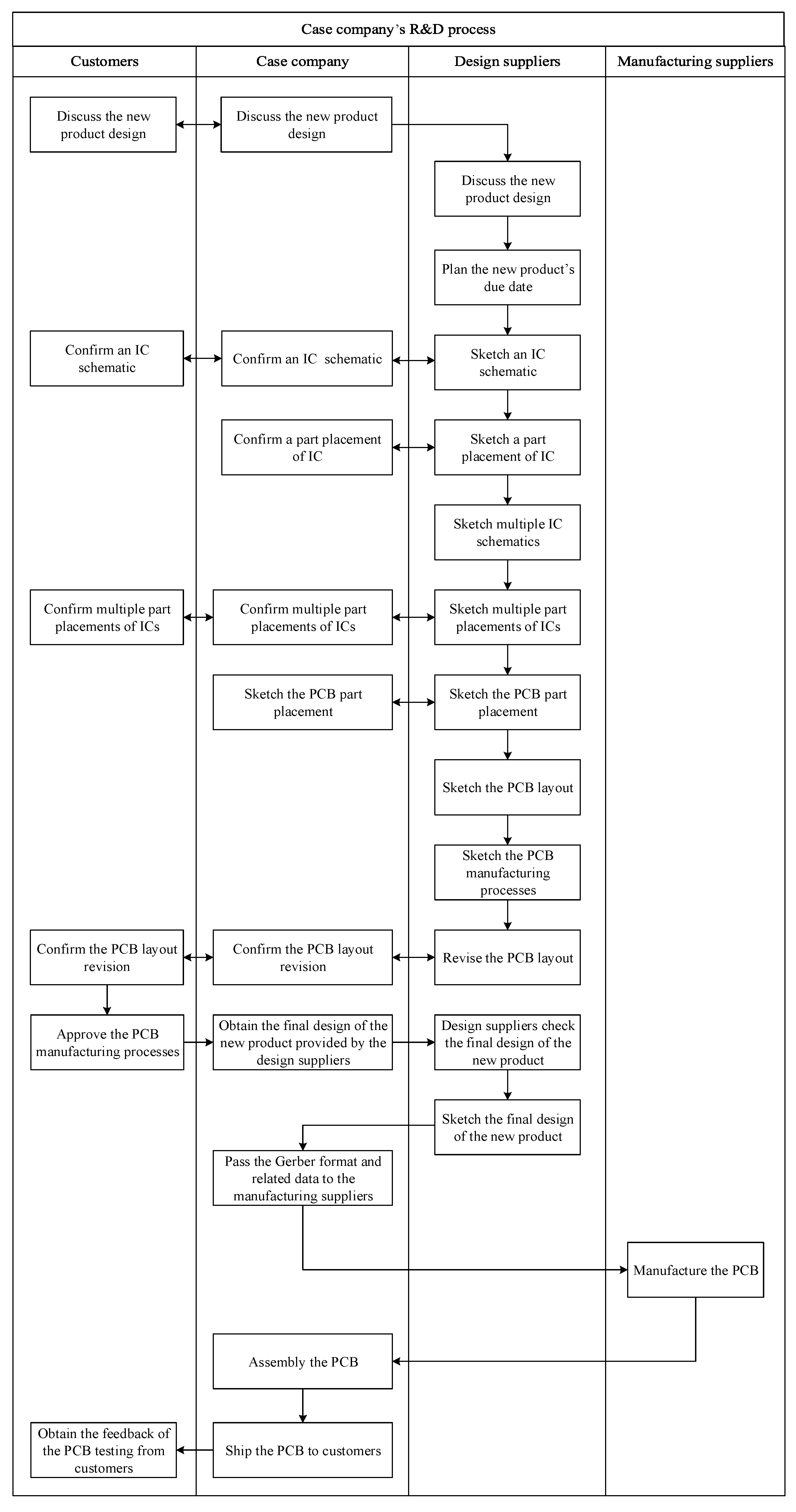
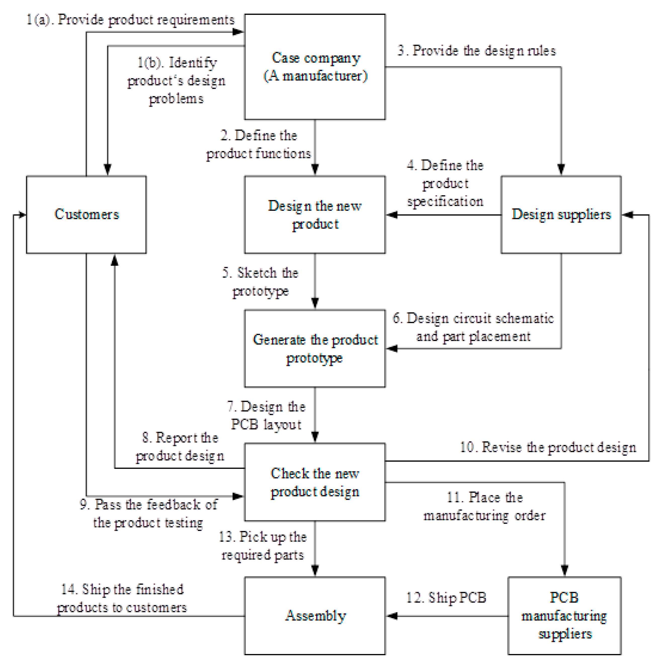
3.1. Background of the Case Company

The major business of the case company includes design, manufacturing, and sales of probe cards used in semiconductor wafer testing. The case company also collaborates with major Japanese companies in the same field to increase the competitiveness of both sides. The case company imported fabrication technologies related to high pin numbers and low pad pitch and became one of the top 10 probe card suppliers. Being a small part of the semiconductor industry, the wafer probe card is one of the wafer testing interfaces created during semiconductor fabrication and is widely used in wafer testing for memory IC, logic IC products, consumer IC products, liquid-crystal display (LCD) driving IC, communication IC products, and electronic instrument and medical equipment IC. Wafer testing can reduce device defects, thereby avoiding the waste in the wafer back-end processes, such as IC packaging. This case company has been the major probe card supplier of many critical wafer fabrication and testing companies.
The cantilever probe card (CPC) and the vertical probe card (VPC) are the two main categories. The case company has set up its CPC design team and VPC design team. IC products tested by CPCs usually have lower levels so their PCBs are mainly designed and made as a customer reference board to reduce the cost and shorten the design and manufacturing time of CPCs. Therefore, the focus of this case study is on improving the VPC to address its higher costs, and longer design and manufacturing times. This research discusses the R&D process of the VPC for the vertical PCB of the case company.
The customer base of the case company is large and includes IC testing and wafer fabrication companies that need to use probe card products. The case company has been playing the role of the leader in recent years to design and make probe cards for world-class manufacturers. This research studies and analyzes the cases of the two customers with maximum orders from the VPC design team.
Customer A of the case company is a main manufacturer of the IC touchpad; 60% of the world’s laptop touchpads are Customer A’s products. The major products of Customer A are consumer IC, LCD control IC, biometrics IC, and touch screen IC. Customers of Customer A are personal computer (PC) original equipment manufacturer (OEM) companies and consumer electronics manufacturers, whose market covers Asian areas from North America. Customer A’s orders account for the highest percentage, at approximately 20%, of the total orders of the case company’s VPC design team. The case company and Customer A have a stable collaboration. Customer A regularly orders a large number of probe cards every year; therefore, both the case company and Customer A pursue perfection in every detail for their common benefits and long-term collaboration. The orders are usually large, so Customer A requests close qualities and designs among projects to ensure a certain level of product design quality. For this reason, the VPC design team of the case company deploys one-tenth of the manpower to manipulate the design-relevant projects and reply to technical questions from Customer A.
Customer B of the case company is the leading company of programmable logic devices (PLD) and occupies more than 90% of the market with its products. PLD can be categorized as field programmable gate array (FPGA), complex programmable logic device (CPLD), and other relative software design tools. The major applications of the chips produced by Customer B are communication, network, and PC equipment, and Customer B allows its customers to design their own programmable logic chips and customize all sorts of IC products. Customer B’s total annual orders rank as the second highest percentage, at around 13–15%, of the total orders of the case company’s VPC design team. Customer B and the case company also have a stable collaboration on PCB design and manufacturing. Customer B’s high level IC testing products require experienced team members, and the same team members are arranged to take care of Customer B’s projects. A team with the same members of case company’s VPC design team is assigned to design only Customer B’s projects and discuss future relative R&D. Customer B does not allow mistakes in the front-end design for its products, which are ultra-precise; therefore, every step in the design process stages must be verified by Customer B.

3.2. R&D Process of VPC

IC chip testing requires accuracy, rapidity, and cost reduction. Therefore, the case company designs the wafer probe cards in such a way that it can test multiple IC chips at the same time if the test platform structure allows. The key part in a wafer probe card determining the number of IC chips able to be tested simultaneously is the PCB.
New IC chip quality tests are needed after the R&D for a new IC chip. To ensure IC chip qualities, customers will provide circuit diagrams of IC chip relevant substrates and IC chip relevant tables (e.g., IC pin XY coordinate tables and solder ball array tables) of the case company to this research for PCB design and manufacturing.
In the initial state of the project (see Part 1), the salesmen turn in the IC information provided by customers to the VPC R&D department. Then, the VPC R&D department transforms the information from the customer into the forms written in the internal common language and tables of the case company; it also evaluates if the probe fabrication capability of the case company satisfies the IC product testing needs of the customer. If the answer is yes, the VPC R&D department will send the information to the VPC mechanical engineering sector to evaluate and design stiffeners and the part keep-out area. After the mechanical engineering sector finishes the relevant mechanical design diagrams and tables (including stiffeners, stiffener mounting holes, part keep-out area, height limits, and other relevant design requirements), they are sent to the PCB R&D team for evaluation. This evaluation integrated the works by the VPC R&D department and the mechanical engineering sector, including the information of pricing, layer numbers, specifications, and time needed for design and manufacturing of the PCB. This information will be sent to the sales department and the customer for their consideration. When customers place orders, they provide complete design information, such as the arrangement coordinates on the wafer, testing speeds and frequencies, and other special requests. The VPC R&D department then sends the design information integrated from the customer’s information to the mechanical engineering sector and PCB R&D department (the major department managing the whole PCB R&D project). The mechanical engineering sector needs to complete the relevant mechanical design of PCB testing by estimating the machine depth, mechanical parts, and corresponding stresses. The three departments examine the diagrams, confirm the design completeness, and send the design to the customer for the final evaluation. Once the customer agrees, the company starts manufacturing the PCBs, assembling the parts, inspecting and checking them, and delivering the finished PCBs to the customer. The case company also keeps tracking the customer’s usage experiences.
The PCB R&D department usually communicates and discusses with the PCB design house the relevant engineering problems of PCB design, such as PCB fabrication limits, special needs during PCB testing, and the materials required for the PCB. The time needed for the case company to communicate and clarify the relative engineering problems with the PCB design companies is two to three days. The design company starts the work after explicating the details of PCB design and manufacturing. Usually, the three major parts of PCB design are circuit schematic, part placement, and PCB layout.
(1) Circuit Schematic
It takes three days for the outsourcing PCB manufacturing to finish sketching a wafer circuit schematic, which is then verified by both the PCB R&D department and the design department of the case company. The PCB R&D department provides feedback (i.e., go or no-go) to the outsourcing company. If it is a go, the outsourcing company expands the sketch to multiple wafer testing circuit schematics, which are again sent to the PCB R&D department. The circuit schematics are then verified by the customer. After the customer’s approval, the outsourcing company is allowed to continue the PCB design. It takes nine to twelve work days from the expansion of the wafer circuit schematic to the customer’s approval.
(2) Part Placement
After the customer provides approval, the outsourcing manufacturer moves on to the part placement step, in which the information the case company provides is integrated and implanted, including mechanical design diagrams, part keep-out area, part specifications, and part locating height limits. Once the part placement is done after four to five work days, the outsourcing manufacturer verifies the arrangement and specification of the part placement with the case company’s R&D department to see if they match the fabrication ability of the case company and the customer’s original requirements. The R&D department simultaneously confirms with the case company’s mechanical engineering sector and returns the relative information to the outsourcing manufacturer.
(3) PCB Layout
The most important task after validating the circuit diagram and device arrangement is the PCB layout. The PCB layout must make the PCB achieve all the required functions as designed by the customer. For instance, the R&D department must use a simulation system to find the wire width and length matching the impedance controlled by the customer before laying out the PCB; protect important signals by separating these signals or wiring on multiple layers during the PCB layout; and make some crucial signals to arrive at the testing point simultaneously during tests by designing the corresponding wires with the same length. In this step, the outsourcing manufacturer closely communicates with the case company’s R&D department to ensure that the PCB’s performances match the design specifications and achieve the customer’s testing requirements. Therefore, the PCB layout is the most critical and the most time-consuming design step, usually taking two to three weeks of work days.

3.3. Introduction to DCOR Processes

The DCOR model of R&D processes in the PCB industry was constructed from the literature review (see Section 2); the corresponding method, framework, and definitions of the constructed DCOR model are presented in this section. According to the literature, the DCOR model could standardize the entire design process systematically; therefore, this research built up the Level 1 to Level 4 models of the R&D process of the DCOR model of the case company based on the model’s protocol. The DCOR proposed by the SCC has systematic definitions of process specifications from Level 1 to Level 3; however, in Level 4, they are not clearly defined. This research adjusts the framework and structure of Level 4 of the DCOR model based on the characteristics of the case company.
The PCB R&D process within the case company and across the case company’s design chain (Figure 1) needed 92 workdays and 41 workdays, respectively, which was too long to survive in the rapid life cycle of probe cards. Therefore, the case company adopted the DCOR model to improve the PCB R&D process to compete in the rapid life cycle of probe cards.
The case company uses the DCOR model to diagnose the problems for the first step of improvement. This research finds the problems by analyzing the PCB industry’s R&D process of the case company by Level 1 to Level 3 of the DCOR model. The research expands the process items of Levels 1 to 3 of the DCOR model to more detailed process subsets and then builds Level 4 of the DCOR model based on Level 1 to Level 3 of the DCOR model for the realistic situation of the industry. The framework of the R&D process within the PCB industry based on the DCOR model has four fundamental levels, as discussed next.

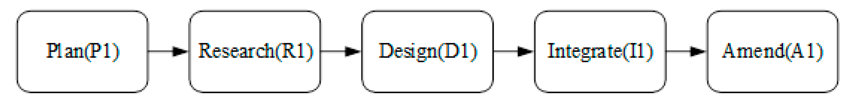
3.3.1. Level 1 of the DCOR Model

Level 1 of the DCOR model has five steps: plan, research, design, integrate, and amend. When building Level 1 of the DCOR model, it must verify the participating members in the design chain. During PCB R&D processes, the integrating and assembling manufacturer (the case company) plays the role of a medium connecting the customer to downstream design companies and fabrication suppliers; therefore, the major members of this design chain are customers, manufacturers, design suppliers, and fabrication suppliers. However, as fabrication suppliers follow a Gerber format to make the bare PCB, which has little influence on the R&D process, fabrication suppliers are not included in the design chain process and do not play an active role in this research. Therefore, the primary members studied in the design chain in this research are customers, manufacturers, and design suppliers. After verifying the members of the design chain for this study, the next step is to build up Level 1 of the DCOR model of the PCB R&D processes, as shown in Figure 2.
(1)
P1: Determine the design chain priority and time of the PCB R&D process.
(2)
R1: The R&D management process includes verifying, decomposing, and clarifying the rules of the R&D project, collecting the design information, and evaluating the feedback of the R&D results. R1 also includes identifying the departments from the design information, designing the methods for using the design information, analyzing the corresponding design and parts, and ensuring that the material and the product specifications satisfy the customer’s needs.
(3)
D1: Design process includes the definitions, productions, simulations, specifications, structures, and functions of products. D1 also contains product manufacturing standards, testing frequency verifications, and product needs.
(4)
I1: Integration process includes deciding the aforementioned product design definition, defining the product design process into a component modulus, releasing the aforementioned R&D process information and its definition, introducing an operating and executing mechanism of the design chain, and cooperating with the customer to provide the design rules to the organization of the downstream design suppliers.
(5)
A1: Track product testing results and improve their R&D process. Track the company’s products to determine if they satisfy customers’ needs and evaluate for future improvement.
The case company is a PCB part assembling company with testing probes as a major product; therefore, the customers are usually wafer fabrication companies. The wafer fabrication companies take probe testing before sawing and packaging wafers to pick out defective wafers in advance, reduce the costs of back-end packaging and testing wafers, and maintain the back-end wafer packaging quality. After making a new wafer product, the wafer fabrication company (the customer) needs to collaborate with the case company on design, produce, and part assembly of the PCB.
In Level 1 of the DCOR model in Figure 3, customers collaborate with the case company to co-organize projects. However, from the customer’s perspective, the case company plays a role as a design company because the case company actually directly discusses the project and design problems with the customers in terms of the design company’s behaviors. The design company does not participate in the project process in the P1 process because it receives instructions on PCB design from the case company.

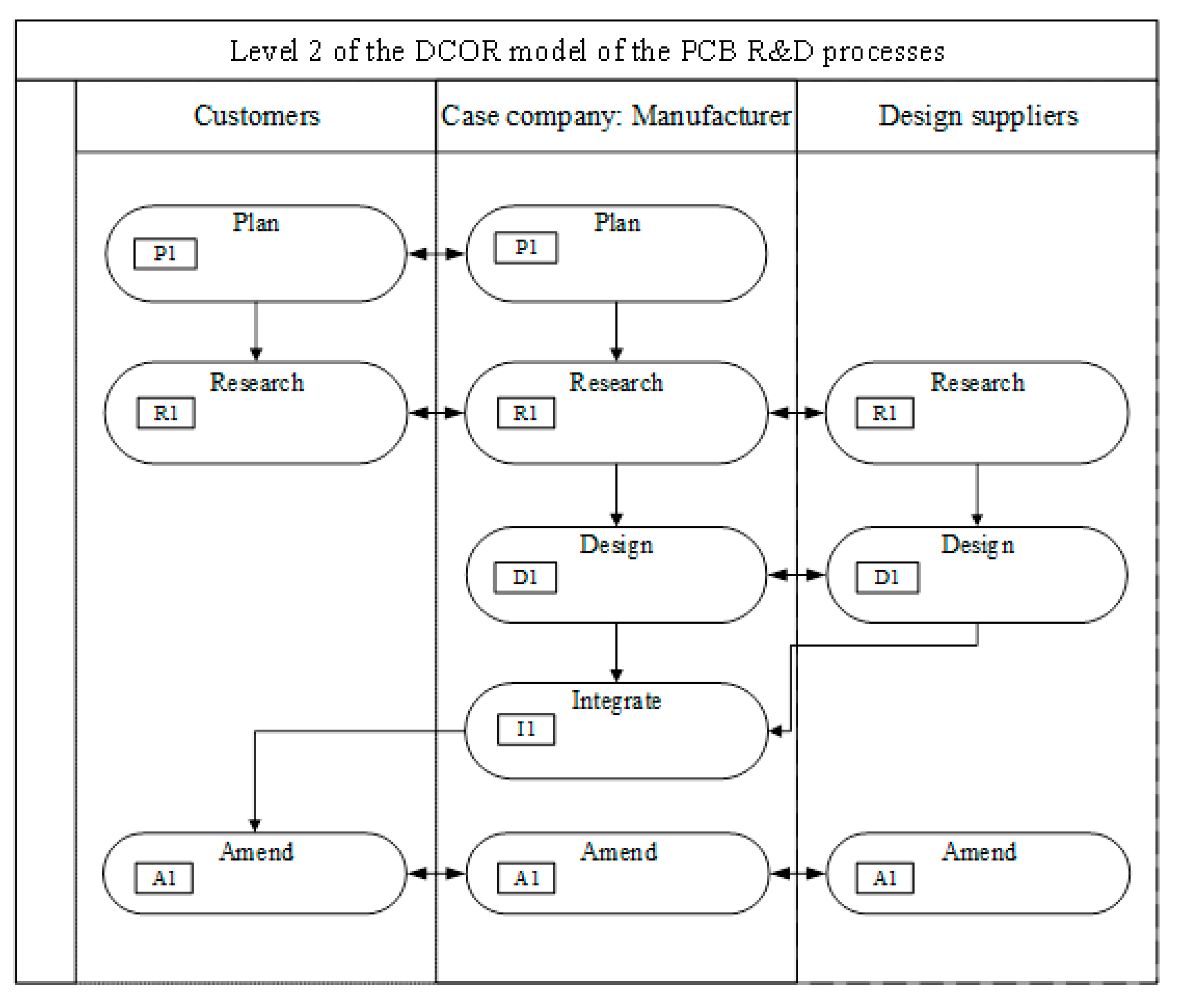
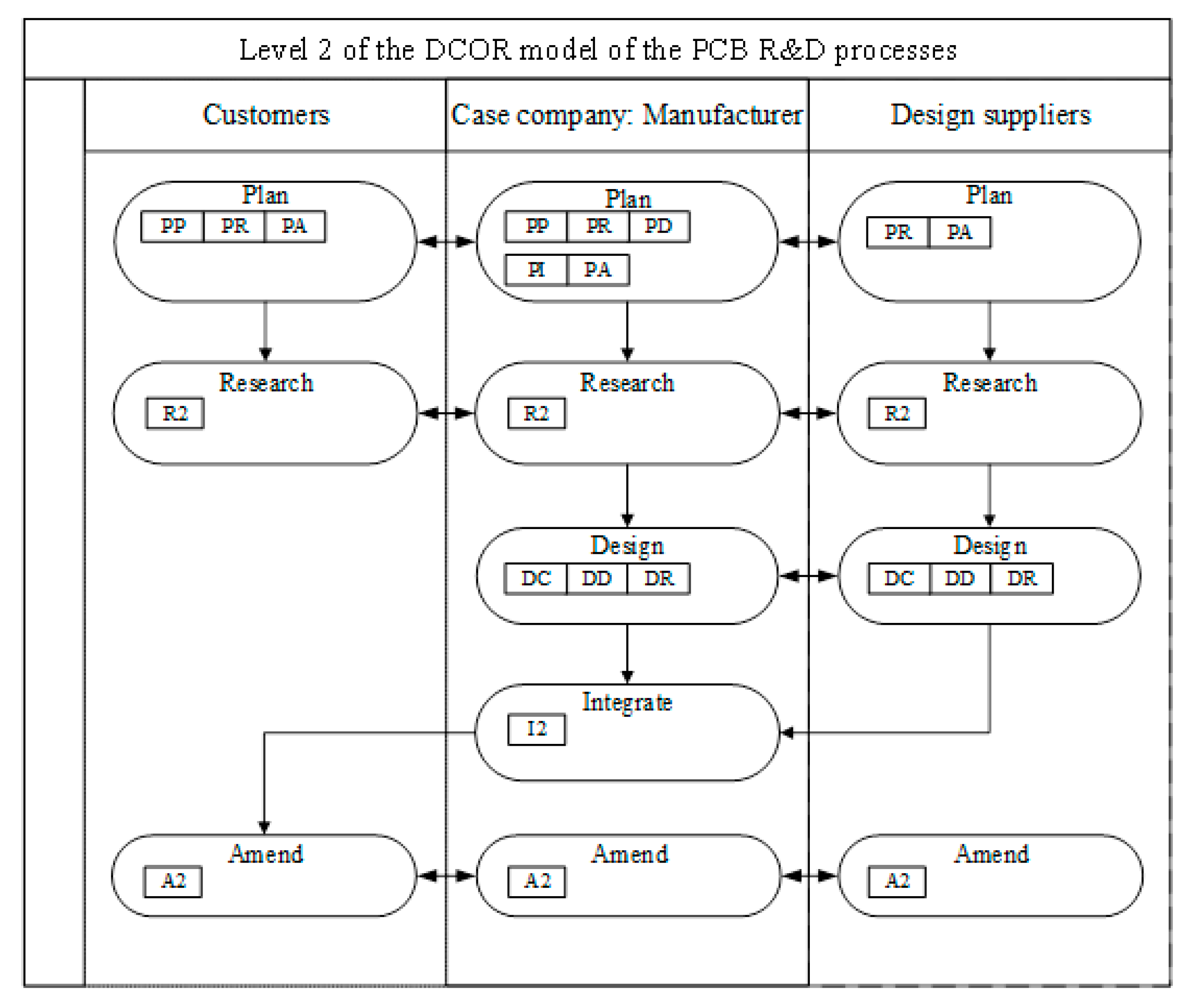
3.3.2. Level 2 of the DCOR Model

The design chain process has different definitions due to product revision, NPD or new fabrication design, and R&D in the DCOR model. Level 2 of the DCOR model is then consequently selected and extended from the design chain domain of Level 1. By extending Level 1 to Level 2 of the DCOR model, this research further discusses and studies of the D1 process in the design chain elements in detail because the major function of the case company is R&D.
In the DCOR model, the R&D of the PCB for testing is part of the NPD process, which is therefore the method of deriving Level 2 of the DCOR model in this research. Level 2 of the DCOR model must confine and verify the domain of the design chain definition as well as judge the research direction of the design chain to see if it is a revision, NPD, or new fabrication R&D from the three design projects of development, design, and integration.
The main topic of the DCOR model study in this research is the R&D of a new PCB product in the case company. Because the case company’s PCB design is specialized for high-end product testing, the PCB design processes have to verify design graphs, specifications, and engineering problems with customers and design companies multiple times to ensure that the design concept and quality match the signal frequencies, impedances, and speeds of IC products that the customer needs to test. However, communication processes result in long waiting times when verifying the solutions of engineering problems and delay the R&D process; therefore, this research analyzes the design chain items using definitions of Level 2 of the DCOR model to improve it.
The case company’s R&D department focuses mainly on planning the integration project of the design chain and new product design, evaluating and verifying the design data viable for fabrication, and then collaborating with the design company to start new product projects. After new product testing, if there are problems from IC testing due to bad design or changes in the customer’s testing needs that results in the need for revision or improvement of the original design, the customer will notify the case company to prepare and carry out design revision with the collaboration of the design company.
As the case company dominates the new product design project, the plan and design need to include plan design chain (PDC), plan design (PD), plan research (PR), plan integrate (PI), and plan amend (PA). On the other hand, the design process covers design concept (DC), design detail (DD), and design review (DR). The case company’s new product projects are independent. Although the new products may share the same type, they usually have different functions and circuit connections. Therefore, this research classified the case company as Level 2 of the DCOR model: R2 (Research New Product), I2 (Integrate New Product), and A2 (Amend Deficient Product).
The design company communicates and discusses with the case company about the relevant design and engineering problems, such as concepts, details, and verification of design, and then provides their internal corresponding project to be verified by the case company. Therefore, in Level 2 of the DCOR model in Figure 4, the design company has Plan: PP, PR, PD, PI, and PA, and Design: DC, DD, and DR.

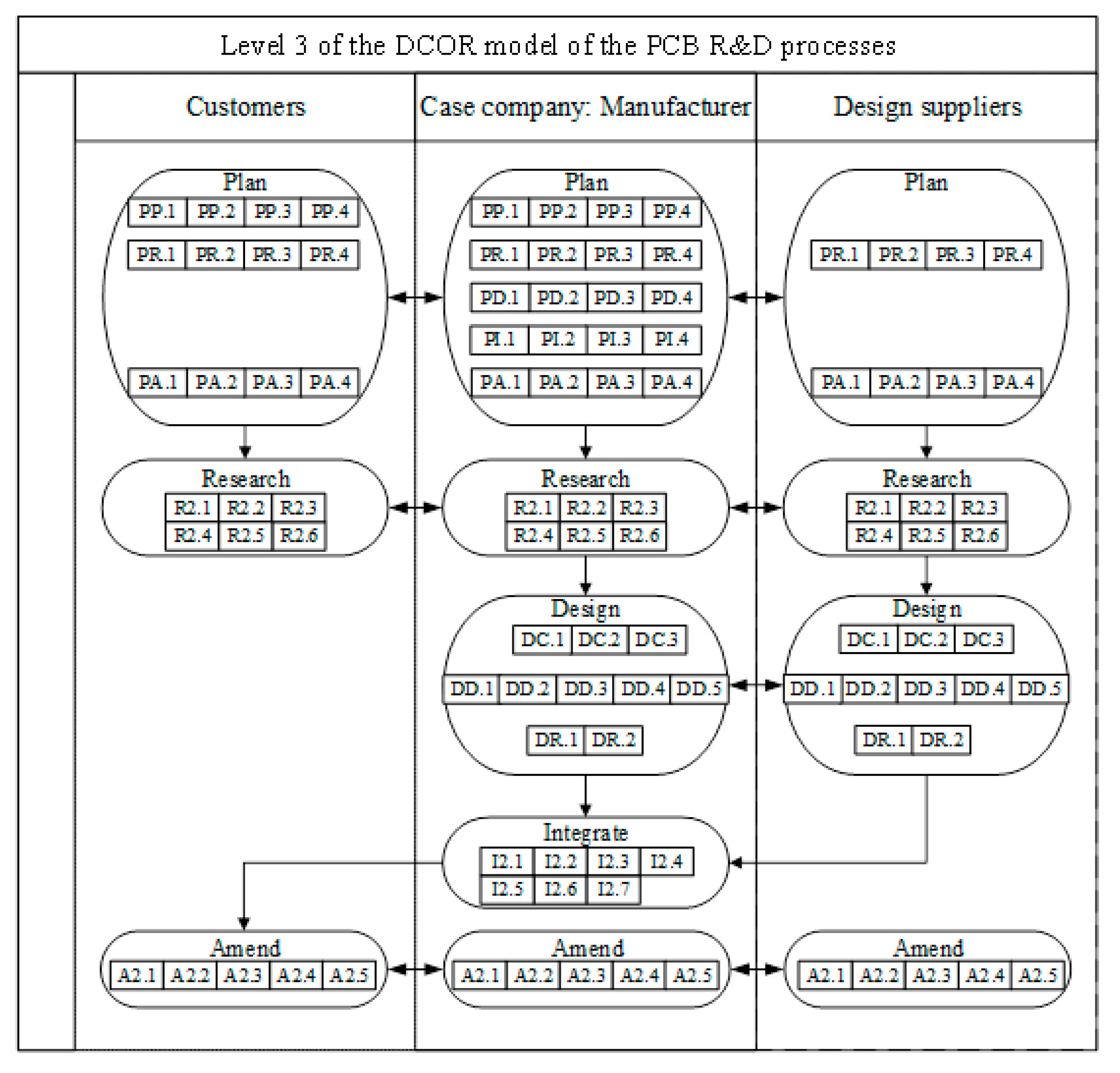
3.3.3. Level 3 of DCOR

According to Level 2 of the DCOR model, the NPD process of the case company needs to define the design items, such as functions of product signals, needs of product frequencies and their corresponding issues derived during design, and adoption of product materials. Complete design rules are then developed using the details expanded from these design items and delivered to the design company to design. For example, the clock (CLK) signals of products must be insulated by a ground line or a ground via so that they will not disturb other normal signals resulting in inaccurate testing results or frequency shifts from signal interferences. When the testing products need to run at high speeds, the product materials must be high end, such as N4000-13 or Rogers, to satisfy the high standards and high speed requirements. When such rules of relevant design items are made and clarified, they continue the PCB prototype building and the subsequent design for simulating PCB prototype testing. After all the processes are confirmed, the design can be released to the customer for verification.
As the medium between the design company and the customers, the case company dominates the process planning of the project R&D process (see Figure 5). The case company evaluates the PCB design’s required data provided by the customer, including test frequencies, test speed, pin function, necessary materials, and fabrication capability. The case company clarifies with the customer the relevant needs and engineering problems related to the product design after a comprehensive evaluation and then makes product design rules after the customer returns the engineering problems and places the order. The case company provides the design rules to the design company for reference and notifies the design company to start the design diagram plotting process.
The design company evaluates design rules and specifications after receiving the design request and discusses relevant engineering problems, design directions, design concepts, and details with the case company. After clarifying the engineering problems, the design company finishes a single IC schematic and sends it to the case company for verification. Once the verification is passed, the design company then starts designing multiple IC schematics, which are also validated after they are finished.
The case company provides mechanical drawings to the design company for the next step placement design only after validating the multiple IC schematics. The case company reconfirms the placements done by the design company; if the placements do not fit the requirements of the case company or customers, the design company needs to correct the placements and repeat the validation procedure with the case company until there is no mistake and the design company can proceed to the next step for PCB layout.
Once PCB layout design is completed, the design diagram is sent to the case company for review. The case company asks the design company to make corrections to its design problems during examination. The case company again reviews the design company’s modification, and then prepares all the design documents, reports, and files for the customer to review. If the customer has concerns or requests modifications of the design, the case company first explains the design philosophy to the customer or returns the design to the design company for modifications. On the other hand, if the customer does not have issues with the design files and approves the PCB fabrication, the case company sends the relevant data and Gerber files to the fabrication suppliers for PCB manufacturing. The case company performs part and probe assembly and outgoing quality control (OQC) after the fabrication suppliers finish and deliver the PCB. The assembled probe card is sent to the customer for wafer testing. When design problems and revision needs emerge during the wafer testing, the customer contacts the case company to request subsequent revisions or design improvements.
Level 3 of the DCOR model expands the details based on Level 2 of the DCOR model. The plan and design are the major R&D processes of the case company mentioned above. The main plan process of Level 3 of the DCOR model is defined as the confirmation of the project, resources needed, resource distribution, and completeness of the entire project, and it further takes the classifications of Level 2 of the DCOR model, such as PP, PD, PR, PI, and PA, as the steps for differentiating and expanding the process. The main design process definition of the case company’s Level 3 of the DCOR model (Figure 6) is to expand DC.1, DC.2, and DC.3 of DC; and DD.1, DD.2, DD.3, and DD.4 of DD; and DR.1 and DR.2 of DR from the last design process step in Level 2 of the DCOR model. This research expands the process structure analysis based on these to ensure that each project has completed a detailed plan and a clear design expansion for the smooth progress of NPD. In addition, NPD processes of the case company can be constructed by using the DCOR model.

3.3.4. Level 4 of the DCOR Model

In this research, Level 4 of the DCOR model’s construction is extended from Level 3 of the DCOR model, which can further classify process elements of new products designed specifically for the case company. The first process element of the case company’s new products is evaluating if the PCB fabrication capability and technology match customers’ expectations. The new product specifications are the major factor in this evaluation for available fabrication capabilities. After verifying the fabrication capability and design concept, this research moves to the next step of making design rule items. The design rules are the guidelines for the design company when designing. The design rule items are the basis of the detailed design regulations for the design company through design rule items, schematic verification, signal functions, and testing results of PCB analysis and simulation. When the PCB design diagram files are finished, the design company provides the case company with the complete schematic, placement, PCB layout, and relevant documents and data reports, such as bills of materials (BOM) tables, wire length reports, and signal impedance simulation reports, for verification. The case company carries out signal simulation analyses and optimizes design modifications. After optimization, the finished design diagram is sent to the customer for approval; once approved, relevant fabrication documents and Gerber files are provided to the PCB fabrication supplier.
In this research, the frameworks of Level 1 to Level 3 of the DCOR model are constructed by the PCB R&D processes. Level 4 of the DCOR model is extended and expanded by Level 3 of the DCOR model based on the new product design process of the case company, which is introduced in Level 3 of the DCOR model as an actual R&D process. Level 4 of the DCOR model’s construction is then based on Level 3 of the DCOR model, as shown in Table 1, Table 2, Table 3, Table 4 and Table 5.

3.4. Summary

Introducing the DCOR model in PCB R&D processes for NPD, design, and management process results in interactive relationships among product planning, design, and improvement in each managing item. This mode introduces the extended framework of the DCOR model to the current R&D process of the case company and further defines detailed and serious design process elements based on this process in order to reduce designers’ conceptual mistakes of product design and misunderstandings of design process as well as risks of inaccurate product design.
The case company’s original NPD processes are independent processes without a system connecting the R&D personnel, which results in the high probability of redesign or reproduction because of design mistakes. After the DCOR model is introduced in the case company, the co-related level framework of NPD process is defined in detail. It turns out that R&D personnel can rapidly and efficiently develop a panoramic view of system frameworks of NPD processes, find defects during NPD projects, further improve and solve problems, improve the NPD process, and ultimately make the NPD process more competitive with advantages.

4. Results and Discussions

The DCOR model in Section 3 can diagnose that many of the time delays in the back-and-forth communication results from too many engineering problem verifications during the NPD process. Too many delays result in the fatal problem of lengthy NPD delivery time, thereby causing the case company to lose competitiveness in the probe card market.
The case company presents the problems by plotting a cause-and-effect chart (Figure 7) and gathers engineers from all the R&D and design departments to brainstorm on improving the R&D process as well as integrate the factors of the aforementioned cause-and-effect chart for the problems of the lengthy R&D process.

4.1. Analysis Steps

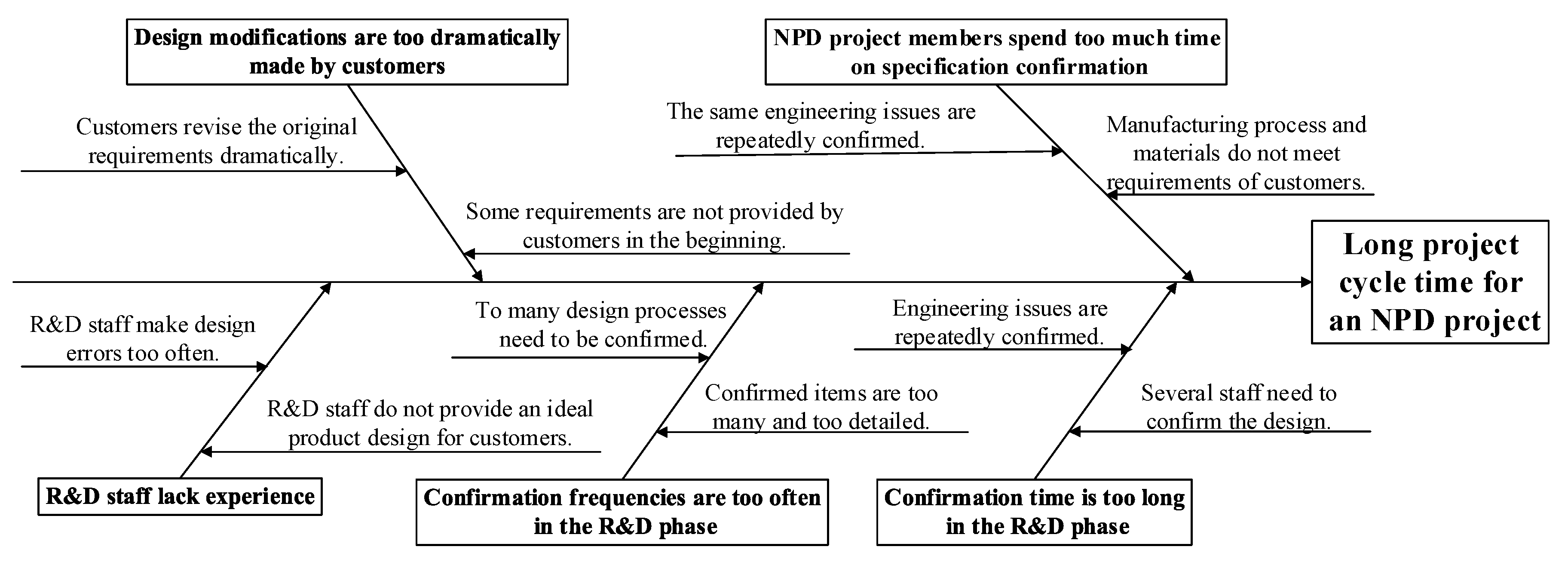
4.1.1. Statement Step

As previously mentioned, the semiconductor design and testing industry changes rapidly, and the delivery time in this industry determine the competitiveness of semiconductor products. A new product developed and designed in a lengthy delivery time does not stay long in the market, so the company gathers engineers to discuss and find solutions through brainstorming to shorten the R&D process delivery time.

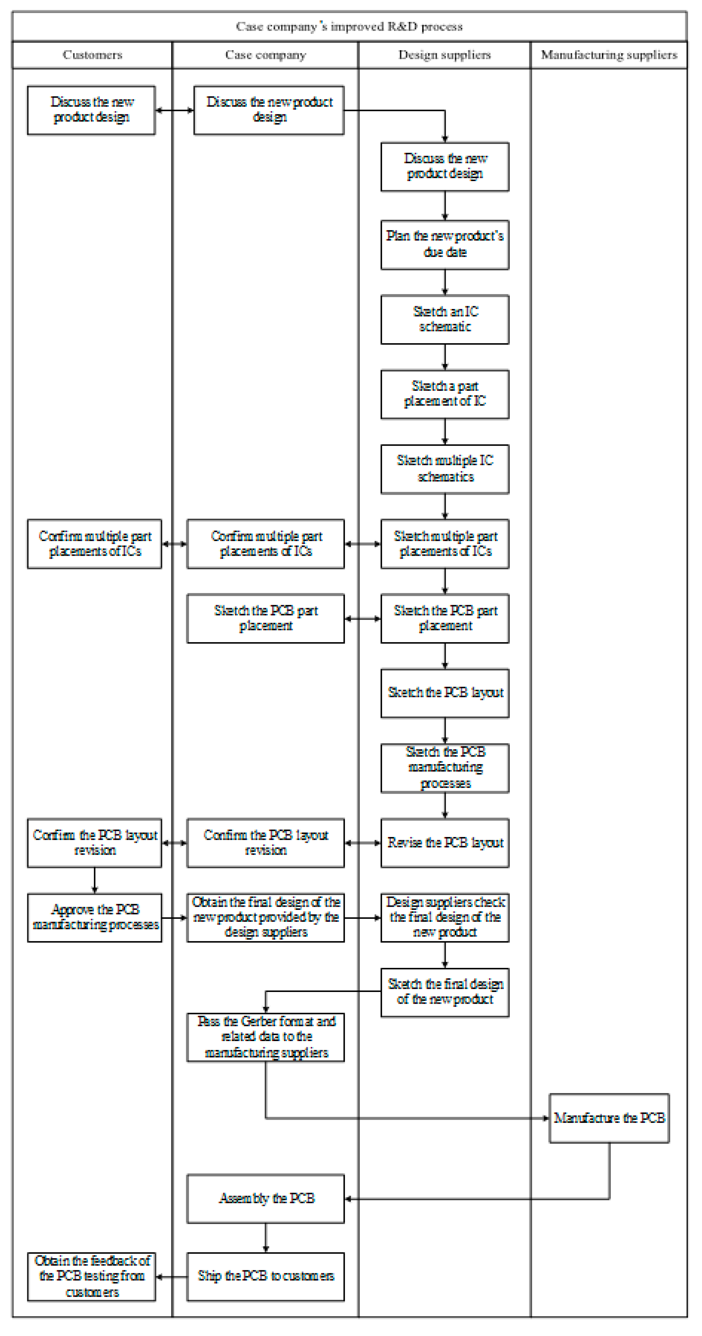
4.1.2. Improvement Step

The case company gathers engineers from all departments to brainstorm on ideas to improve the five major problems from the cause-and-effect chart diagnosed by the DCOR model. The outcomes can be summarized in the following eight solutions:
  • The case company should build up a database for long-term customers’ new product projects to store their new product signals and conventional materials. When customers start discussions about new product needs, the stored data will remind the customers about materials used in the previous product designs and compare the differences between the new products and the previous ones, thereby efficiently reducing the waiting and verification time from repeatedly asking the customers about the same engineering questions.
  • Both the case company and the design company should have their own database to ensure rapid evolving fabrication capability and customer requests as well as decrease the numbers and time of repeated engineering question inquiries. Therefore, they can reveal design data problems and issues needing further reviews and verifications of new products, thereby improving the problems of design process interruptions stemming from engineering mishaps.
  • After the individual databases of the case company and the design company are built up, not many engineers are needed for repeating engineering problem verifications. Engineering problems can be referred to the previous product design data, examined, and responded to by accessing the databases. Designers just need to look up and follow the related examined engineering problems for new designs monitored and verified by a senior engineer during the design process. The goal is to shorten the delivery time, decrease mistake rates, and conserve manpower.
  • The design company follows the models in the database to design and set up specific stages with corresponding inspection items instead of random inspection stages of design schematic files for the case company. Such a method of conducting inspections at fixed stages can reduce the mistake rates of file checking as well as the inspection time, numbers, and error risks of the case company.
  • The case company communicates and discusses potential future revisions of some IC signals and some IC program design with the customer, which is treated exceptionally. After the PCB design is over, it takes less time and fewer efforts to modify the PCB design because of IC program revisions.
  • The case company inquiries about the customer’s ideal PCB design and it notes the corresponding attention in the database before a project. The case company then verifies with the customer each detailed design element and regulation to determine the design goal before starting the design and decreases the scale of revision if the finished design does not fit the customer’s expectation.
  • A senior designer should participate in a new R&D project if possible so that he or she can pass his or her experience from customer’s preferences and ideal design styles to newcomers. In this way, it decreases design errors resulting in quality issues caused by new designers with a lack of experience.
  • The senior designers are asked to create files of checking lists or attention memorandums of design processes for newcomers or designers who never come into contact with certain customers before having design references. During each design process, every designer must fill new customer requests or new special specifications back into these files as references for other designers in future design projects.
The delivery time was shortened by 10 days, from the original 92 days to 82 days, with the cooperation and efforts by the customer, the case company, and the design company. In Figure 8, the case company abbreviated many stages of verifications and inspections by using the aforementioned improvement methods. Originally, both the case company and the design company had to provide design data and diagrams of single IC schematics, IC circuit schematics, and multiple IC integrated element schematics to be verified by the case company. After improvements were made, only the finalized schematics needed to be verified by the customer and the case company. Such an approach to improvements not only shortens the delay time during design examinations, but also reduces design risks from examinations by the customer and the case company, thereby increasing the competitiveness of IC semiconductors and PCB probe cards.

4.2. Discussions

By applying the DCOR model in this case, redundant design elements and actions were identified in the design chain of the case company. This research used the DCOR model with the case company, revealing that too many repeated operational processes resulted in lengthy delivery times. The case company then discussed and analyzed the diagnosed problems and elements and further brainstormed to propose a better solution for improving these problems. This method not only effectively shortened the product design delivery time of Customer A, but also reduced the risks and problems during the design process.
The case company obtained a different result when following the same design process and improvement method applied to Customer B’s R&D process. Customer B’s R&D process time only decreased by two days, from 92 days to 90 days. The analysis indicated the main reason was that Customer B did not agree to reduce the steps of design diagram verifications, so that the case company could not reduce the delay time when the design company waited for Customer B to verify the diagrams. Therefore, the method of brainstorming could not be used in Customer B’s R&D process. Although the case company could not reduce Customer B’s R&D process, it could still increase the design quality of Customer B. In addition, because of the new built-up database, filed design process, and attention notes done by the case company, Customer B’s new product R&D has better self-consistency and satisfaction of the customer’s expectations than the previous R&D efforts before improving.

4.3. Summary

The design chain R&D process is not the responsibility of only one department, but it is a collaboration involving up-stream and down-stream partners to smoothly progress a process improvement. Using Customers A and B in this research as examples, Customer A was willing to improve the project process with the case company and the design company, resulting in a shortened delivery time of R&D by 10 days, from 92 days to 82 days. Thus, Customer A’s IC products gain better competition advantages in the market.
Although Customer B was not willing to abbreviate the steps of design diagram verifications, this project still helped ensure that each step of Customer B’s product design diagrams were effectively monitored, paused, and modified when unexpected changes happened. Customer B’s decision somehow still provided an additional mechanism for monitoring its product design and manufacturing.
Comparing the analyses of these two cases, one can conclude that R&D and design process improvement require all members’ efforts and collaborations, and the key success factors include supports from the administrators and customers, capabilities of professional teams, communication and collaboration among departments, the same goals, education and training, as well as process reconstructions. Davenport et al. [3] indicated that enterprises should evaluate all kinds of needs globally and then think broadly about the usages of IT technologies. In other words, so-called modes or improvement methods target enterprise optimization; thus, an enterprise can evaluate and reconstruct itself through its product design priorities. Moreover, the approach is well explained in the international scenario, referring to Kugler’s [35] research.

5. Conclusions

This research applies the DCOR model to the case company to expand the design chain processes, improve the problems of the R&D process through brainstorming, and discuss and effectively study a method to achieve the ultimate goals of shortening delivery time while simultaneously reducing risks and errors during the design process. Through the collaboration of Customer A, the case company, and the design company, the new product delivery time was shortened by 10 days, from 92 days to 82 days; in addition, its R&D competitiveness was increased, and the case company earned more advantages for future orders from this customer, which eventually resulted in a win–win situation. Having improved the R&D process, the case company now faces the challenges of using new fabrication technologies and strengthening its competitive advantages. It is a practice of the R&D process and efficiency management visions of the case company to realize the importance of process improvement, make the process clear in definitions, and further proceed the enterprise’s process in the future.
Potential future research can extend further, improving the design chain manufacturing cycle time to generate more competitive advantages of new products. In addition to customers’ processes, quality problem improvements emphasizing production, manufacturing, and assembling as well as the design part can not only shorten design and manufacturing periods, but also increase product yield rates and reduce costs, thereby increasing the company’s competitive advantages. In the future, generalizations of product competitiveness enhancement potential in the rapid proceeding of technology can be extended to include a variety of applications.

Author Contributions

P.-S.C. contributed to manuscript preparation, experiment planning, and experiment measurements. J.C.-M.C. contributed to writing and original draft preparation. W.-T.H. contributed to data analysis, review, and editing. L.-Y.K. contributed to research sample preparation. All authors have read and agreed to the published version of the manuscript.

Funding

This research received no external funding.

Conflicts of Interest

The authors declare no conflict of interest.

References

  1. Farrukh, C.; Fraser, P.; Gregory, M. Development of a structured approach to assessing practice in product development collaborations. Proc. Inst. Mech. Eng. Part B J. Eng. Manuf. 2003, 217, 1131–1144. [Google Scholar] [CrossRef]
  2. Ganotakis, P.; Hsieh, W.L.; Love, J.H. Information systems, inter-functional collaboration and innovation in Taiwanese high-tech manufacturing firms. Prod. Plan. Control. 2013, 24, 837–850. [Google Scholar] [CrossRef] [Green Version]
  3. Davenport, T.H.; Short, J.E. The new industrial engineering: Information technology and business process redesign. MIT Sloan Manag. Rev. 1990, 31, 11–27. [Google Scholar]
  4. Song, W.Y.; Cao, J.T.; Zheng, M.K. Towards an integrative framework of innovation network for new product development project. Prod. Plan. Control. 2016, 27, 967–978. [Google Scholar] [CrossRef]
  5. Wang, F.K.; Yeh, C.T.; Chu, T.P. Using the design for Six Sigma approach with TRIZ for new product development. Comput. Ind. Eng. 2016, 98, 522–530. [Google Scholar] [CrossRef]
  6. Zhang, C.; Zhou, G.H.; Lu, Q.; Chang, F.T. Graph-based knowledge reuse for supporting knowledge-driven decision-making in new product development. Int. J. Prod. Res. 2017, 55, 7187–7203. [Google Scholar] [CrossRef]
  7. Švarcová, J.; Urbánek, T.; Povolná, L.; Sobotková, E. Implementation of R&D results and industry 4.0 influenced by selected macroeconomic Indicators. Appl. Sci. 2019, 9, 1846. [Google Scholar]
  8. Li, D.C.; Yeh, C.W.; Chen, C.C.; Shih, H.T. Using a diffusion wavelet neural network for short-term time series learning in the wafer level chip scale package process. J. Intell. Manuf. 2016, 27, 1261–1272. [Google Scholar] [CrossRef]
  9. Li, J.; Gu, J.; Huang, Z.; Wen, J. Application research of Improved YOLO V3 algorithm in PCB electronic component detection. Appl. Sci. 2019, 9, 3750. [Google Scholar] [CrossRef] [Green Version]
  10. Lv, S.; Xian, R.; Li, D.; Zheng, B.; Jin, H. An FCM–GABPN ensemble approach for material feeding prediction of printed circuit board template. Appl. Sci. 2019, 9, 4455. [Google Scholar] [CrossRef] [Green Version]
  11. Noori, H.; Lee, W.B. Collaborative design in a networked enterprise: The case of the telecommunications industry. Int. J. Prod. Res. 2004, 42, 3041–3054. [Google Scholar] [CrossRef]
  12. Fagerstrom, B.; Jackson, M. Efficient collaboration between main and sub-suppliers. Comput. Ind. 2002, 49, 25–35. [Google Scholar] [CrossRef]
  13. Oh, J.; Lee, S.; Yang, J. A collaboration model for new product development through the integration of PLM and SCM in the electronics industry. Comput. Ind. 2015, 73, 82–92. [Google Scholar] [CrossRef]
  14. Marmier, F.; Gourc, D.; Laarz, F. A risk oriented model to assess strategic decisions in new product development projects. Decis. Support Syst. 2013, 56, 74–82. [Google Scholar] [CrossRef] [Green Version]
  15. Supply-Chain Council. Design-Chain Operations Reference-Model; Version 2.0.; Supply-Chain Council: Pittsburgh, PA, USA, 2009. [Google Scholar]
  16. Booz, Allen & Hamiton. New Products Management for the 1980s; Booz, Allen & Hamiton: New York, NY, USA, 1982. [Google Scholar]
  17. Ullman, D.G. The Mechanical Design Process; McGraw-Hill: New York, NY, USA, 1992. [Google Scholar]
  18. Cooper, R.G. Perspective third generation new product process. J. Prod. Innov. Manag. 1994, 11, 3–14. [Google Scholar] [CrossRef]
  19. Baxter, M. Product Design: Practical Methods for the Systematic Development of New Products; CRC Press: New York, NY, USA, 1995. [Google Scholar]
  20. Gerhard, P.; Wolfgang, B. Engineering Design: A Systematic Approach; Springer: New York, NY, USA, 1988. [Google Scholar]
  21. Lee, C.W.; Suh, Y.; Kim, I.K.; Park, J.H.; Yun, M.H. A systematic framework for evaluating design concepts of a new product. Hum. Factors Ergonom. Manuf. Serv. Ind. 2010, 20, 424–442. [Google Scholar] [CrossRef]
  22. Chen, W.C.; Chang, H.P.; Lin, K.M.; Kan, N.H. An efficient model for NPD performance evaluation using DEMATEL and fuzzy ANP-applied to the TFT-LCD touch panel industry in Taiwan. Energies 2015, 8, 11973–12003. [Google Scholar] [CrossRef] [Green Version]
  23. Chen, W.C.; Wang, L.Y.; Lin, M.C. A hybrid MCDM model for new product development: Applied on the Taiwanese LiFePO4 industry. Math. Probl. Eng. 2015, 462915–462929. [Google Scholar]
  24. Kumar, S.; Luthra, S.; Govindan, K.; Kumar, N.; Haleem, A. Barriers in green lean six sigma product development process: An ISM approach. Prod. Plan. Control. 2016, 27, 604–620. [Google Scholar] [CrossRef]
  25. Shih, W.Y.C.; Agrafiotes, K.; Sinha, P. New product development by a textile and apparel manufacturer: A case study from Taiwan. J. Text. Inst. 2014, 105, 905–919. [Google Scholar] [CrossRef]
  26. Sondergaard, E.; Oehmen, J.; Ahmed-Kristensen, S. Extension of internationalisation models: Drivers and processes for the globalisation of product development—A comparison of Danish and Chinese engineering firms. Prod. Plan. Control. 2016, 27, 1112–1123. [Google Scholar] [CrossRef] [Green Version]
  27. Ying, C.S.; Li, Y.L.; Chin, K.S.; Yang, H.T.; Xu, J. A new product development concept selection approach based on cumulative prospect theory and hybrid-information MADM. Comput. Ind. Eng. 2018, 122, 251–261. [Google Scholar] [CrossRef]
  28. Sastoque Pinilla, L.; Llorente Rodríguez, R.; Toledo Gandarias, N.; López de Lacalle, L.N.; Ramezani Farokhad, M. TRLs 5–7 advanced manufacturing centres, practical model to boost technology transfer in manufacturing. Sustainability 2019, 11, 4890. [Google Scholar] [CrossRef] [Green Version]
  29. MacKerron, G.; Kumar, M.; Benedikt, A.; Kumar, V. Performance management of suppliers in outsourcing project: Case analysis from the financial services industry. Prod. Plan. Control. 2015, 26, 150–165. [Google Scholar] [CrossRef]
  30. Georgise, F.B.; Wuest, T.; Thoben, K.D. SCOR model application in developing countries: Challenges & requirements. Prod. Plan. Control. 2017, 28, 17–32. [Google Scholar]
  31. Choi, Y.H.; Kim, K.; Kim, C. A design chain collaboration framework using reference models. Int. J. Adv. Manuf. Technol. 2005, 26, 183–190. [Google Scholar] [CrossRef]
  32. Lin, J.; Juan, Y.; Ou-Yang, C. A DCOR-based MAS framework to support design chain cooperation. In Proceedings of the 12th International Conference on Computer Supported Cooperative Work in Design, Xi’an, China, 16–18 April 2008; pp. 323–329. [Google Scholar]
  33. Zuñiga, R.; Seifert, M.; Thoben, K.D. Study on the application of DCOR and SCOR models for the sourcing process in the mineral raw material industry supply chain. In Dynamics in Logistics-Proceedings of LDIC 2012 Bremen, Germany; Kreowski, H., Scholz-Reiter, B., Thoben, K.D., Eds.; Springer: Berlin/Heidelberg, Germany, 2013; pp. 211–220. [Google Scholar]
  34. Ahoa, E.; Kassahun, A.; Tekinerdogan, B. Configuring supply chain business processes using the SCOR reference model. In Business Modeling and Software Design; Shishkov, B., Ed.; Springer: Cham, Switzerland, 2018. [Google Scholar]
  35. Kugler, H. Blütenökologische Untersuchungen mit Hummeln. IX. Die optische nahwirkung von natürlichen blüten und blütenständen. Planta 1938, 29, 47–66. [Google Scholar] [CrossRef]
Figure 1. Flowchart of PCB R&D process across the case company’s design chain.
Applsci 10 03703 g001
Figure 2. Level 1 of the DCOR model.
Applsci 10 03703 g002
Figure 3. Level 1 of the DCOR model of the PCB R&D processes.
Applsci 10 03703 g003
Figure 4. Level 2 of the DCOR model of the PCB R&D processes.
Applsci 10 03703 g004
Figure 5. New PCB R&D process.
Applsci 10 03703 g005
Figure 6. Level 3 of the DCOR model of the PCB R&D processes.
Applsci 10 03703 g006
Figure 7. Cause-and-effect chart of the PCB R&D process.
Applsci 10 03703 g007
Figure 8. Improved R&D process across the case company’s PCB design chain.
Applsci 10 03703 g008
Table 1. Plan process of DCOR Level 4.
Level 3Plan Process Descriptions of DCOR Level 4
PP.1PP.1.1Plan a NPD project planning
PP.2PP.2.1Plan the NPD required resources, software, and display planning
PP.3PP.3.1Plan the NPD R&D project, staff, and project length planning
PP.4PP.4.1Key in the data of the NPD planning into the information system
PR.1PR.1.1Confirm the manufacturing process capability for new products and the R&D capability for new components
PR.2PR.2.1Confirm the NPD R&D resources, software, and equipment
PR.3PR.3.1Confirm the allocation of the staff and time for the NPD project
PR.4PR.4.1Confirm the technological data and the R&D plan of the NPD project
PD.1PD.1.1Confirm the NPD requirements and order requests
PD.2PD.2.1Evaluate the ability of R&D engineers and confirm the manufacturing process technology for the NPD project
PD.3PD.3.1Allocate the R&D engineers, software, and raw materials for the NPD project
PD.4PD.4.1Key in the NPD execution plan into the information system
PI.1PI.1.1Plan products’ integrated component requirement planning
PI.2PI.2.1Negotiate the allocation of products’ integrated time, raw materials, staff, and production assembly lines
PI.3PI.3.1Confirm the allocation of products’ integrated time, raw materials, staff, and production assembly lines
PI.4PI.4.1Key in the project integrated execution plan into the information system
PA.1PA.1.1Collect the data of the improved requests
PA.2PA.2.1Analyze the cause-and-effect and solutions for the improved requests
PA.3PA.3.1Allocate resources, staff, and tasks for implementing the improved project
PA.4PA.4.1Key in the improved project items and the modified requirements into the information system
Table 2. Research process of DCOR Level 4.
Level 3Research Process Descriptions of DCOR Level 4
R2.1R2.1.1Initialize the kick-off meeting of the NPD R&D project and confirm the NPD manufacturing process specifications
R2.2R2.2.1Decide the NPD R&D schedule
R2.2.2Propose the collaboration plan with the PCB design suppliers
R2.3R2.3.1Confirm the NPD manufacturing process data
R2.4R2.4.1Verify the NPD R&D manufacturing process capability of the case company
R2.4.2Verify the design capability of the PCB design suppliers
R2.5R2.5.1Release the NPD R&D results and transfer the associated document to the PCB design suppliers
R2.5.2Review the NPD R&D results
R2.6R2.6.1Authorize the PCB design suppliers to design and manufacture PCB products
Table 3. Design process of DCOR Level 4.
Level 3Design Process Descriptions of DCOR Level 4
DC.1DC.1.1Confirm the product specification of the new product design
DC.1.2Confirm the conceptual schematics of the new product
DC.1.3Confirm the analysis function of the new product simulation
DC.2DC.2.1Confirm the design items of the new product design
DC.2.2Confirm the manufacturing process capability of the new product design
DC.2.3Confirm the key components’ layout of the new product design
DC.3DC.3.1Confirm the design activities’ schedule of the new product design
DD.1DD.1.1Discuss the evaluation rules for the new product design
DD.1.2Discuss the guidelines for the new product design
DD.1.3Confirm the guidelines for the new product design
DD.2DD.2.1Draw the component connected design in the signal function diagram of the new product
DD.2.2Draw the circuit connected design in the signal function diagram of the new product
DD.3DD.3.1Simulate the optimization design for testing the new product
DD.3.2Simulate the impedance specifications of the new product
DD.4DD.4.1Design the component layout design of the new product
DD.4.2Design the structure layout design of the new product
DD.4.3Discuss the circuit layout design of the new product
DD.4.4Modify the layout design of the new product
DR.1DR.1.1Write the detailed document of the new product’s schematics
DR.1.2List the new product layout diagrams
DR.1.3Delete unnecessary auxiliary boxes in the new product layout diagram
DR.2DR.2.1Check the details of the new product’s design diagram
DR.2.2Generate the final schematics of the new product design
DR.2.3Generate the final layout of the new product design
DR.2.4Generate the final structure layout of the new product design
DR.2.5Generate the final circuit layout of the new product design
DR.2.6Generate the final components’ BOM of the new product design
DR.2.7Generate the product specifications of the new product design
Table 4. Integrate process of DCOR Level 4.
Level 3Integrate Process Descriptions of DCOR Level 4
I2.1I2.1.1Write the new product’s document
I2.1.2Evaluate the feasibility of the new product
I2.1.3Confirm the new product’s requirements
I2.2I2.2.1Decide the associated tasks and rules for the new product
I2.2.2Check the main functions of the new product
I2.2.3Decide the alternatives for the new product’s special tasks
I2.2.4Evaluate the confidence level of the new product’s design
I2.2.5Decide the product’s estimated production schedule
I2.3I2.3.1Integrate machine resources for manufacturing the new product
I2.3.2Integrate production lines for manufacturing the new product
I2.3.3Integrate due date requirements for manufacturing the new product
I2.4I2.4.1Integrate operations for manufacturing the new product
I2.4.2Define the new product’s design specification
I2.5I2.5.1Review the new product specification
I2.5.2Release the new product specification
I2.5.3Report the new product’s testing results
I2.6I2.6.1Examine the final version of the new product specification
I2.6.2Package the new product
I2.7I2.7.1Deliver the finished product to customers
Table 5. Analyze process of DCOR Level 4.
Level 3Analyze Process Descriptions of DCOR Level 4
A2.1A2.1.1Trace the product design defects by customers’ feedbacks
A2.1.2Summarize the reasons of customers’ complaints for requesting product design modification
A2.2A2.2.1Analyze the effects of the product design defects and product design modification
A2.3A2.3.1Analyze, improve, and prioritize the product design defects
A2.4A2.4.1Assign the defective products to the associated departments based on the classification of the product design failures for improvement
A2.4.2Reevaluate the feasibility verification and the improved report proposed by the staff who make product design defects
A2.5A2.5.1Define the product design rules and product modification rules for future product design guidelines

