1. Introduction
Calcium copper titanate (CaCu
3Ti
4O
12, CCTO) has received widespread attention as an excellent electroceramic material for potential applications in capacitor, memory, sensor, microelectronic, and energy storage devices [
1,
2,
3,
4,
5]. CCTO is part of the Im3 space group with a pseudo-cubic perovskite structure, and in the unit cell the lattice parameter is 7.391 Å, presenting an extraordinarily high dielectric permittivity (
) and moderate dielectric loss (tan
) [
6]. In the year 2000, Subramanian et al. reported colossal dielectric constants (up to 10
5) of the ACu
3Ti
4O
12 type (A = Ca, Sr, Ba, La, Bi, Nd). The huge value of
is almost independent of frequency in a broad range up to 10
6 Hz, showing good phase stability in the temperature range of 20–600 K. This exceptional behavior could be attributed to a polarizability mechanism related with the peculiar CCTO crystal structure [
7]. A completely satisfactory explanation is not yet available for this novel dielectric performance. To date, several models have been proposed to explain the origin of the large dielectric permittivity of CCTO. Among them, the generally accepted view is that the behavior is not intrinsic, and the high
value could be ascribed to conducting grains with insulating grain boundaries through the internal barrier layer capacitance (IBLC) mechanism [
8]. The IBLC model has been generally accepted by most researchers, and it supposes that CCTO includes two parts: semiconducting grains and insulating grain boundaries. The grains work as electrodes of micro-capacitors connected in series and the grain boundaries contribute to the dielectric [
9]. Adams et al. [
10] used impedance spectroscopy (IS) to investigate the electrical microstructure of CCTO ceramics and demonstrated that they are electrically inhomogeneous, containing semiconducting grains with insulating grain boundary regions. Furthermore, compared with traditional ceramics like barium titanate or Lead Zirconium Titanate (Piezoelectric ceramic materials) (PZT) [
11,
12], CCTO demonstrates high dielectric losses and low breakdown voltage, which has been the main focus of researchers.
Based on the IBLC mechanism, a great number of theoretical and experimental studies have been carried out to further improve the performance of CCTO. Various processing routes to synthesize CCTO were adopted, such as high-temperature solid-state reaction, soft-chemistry, sol–gel, co-precipitation, microwave heating, and mechanical mixing methods [
13,
14,
15,
16,
17]. Solid-state reactions with the prerequisite of high temperature represent a common method for the preparation of CCTO from the powders of CaCO
3 or CaO, CuO, and TiO
2, with long reaction times [
18,
19]. This method normally requires at least two steps to react in the furnace: one is calcination close to 1000 °C for 8–12 h, and the other is sintering at 1150 °C for more than 10 h, which can produce pure CCTO. Even so, the solid-state route suffers the disadvantages of inhomogeneity and complex repetitive ball milling with prolonged reaction times at higher temperatures. In contrast, the laser irradiation process only needs seconds or minutes. Conventional methods usually involve the excessive consumption of energy and are not suitable for mass production. Other soft-chemistry methods, such as sol–gel and co-precipitation, allow synthesis of CCTO at a relatively low temperature with a shorter reaction time. Although the resultant is homogeneous in stoichiometric ratio at the atomic scale, the final acquisition of pure CCTO is inseparable from the processes of calcination and sintering in furnaces at high temperatures [
20,
21,
22].
Here, we adopted a rapid laser reactive sintering method to synthesize CCTO, substituting the conventional furnace. With a focused laser beam through a convex lens directed on precursors, the reactive sintering time can be significantly reduced down to several minutes or seconds, while guaranteeing a good crystal structure and high dielectric permittivity of CCTO. Rapid laser reactive sintering is suitable for those materials which are hard to manufacture by a conventional solid-state reactions in furnaces. This method is a low-cost approach, with minimal processing steps which can be performed in various environments, such as air, oxygen, or inert gases, according to actual demand. In this work, CCTO synthesized by rapid laser reactive sintering method exhibited high dielectric permittivity and moderate dielectric loss at a wide frequency range, with good frequency stability. The microstructure, grain, and grain boundary resistance were analyzed by studying the impedance spectroscopy, and the conduction mechanism of CCTO was discussed based on an equivalent circuit consisting of resistors and capacitors for semiconducting grains and insulating grain boundaries. The activation energies for the grain boundaries were deduced according to the relationship of ln versus 1/T.
3. Results and Discussion
Figure 2 shows XRD spectra of the CCTO ceramics by laser sintering at various laser power rates. The main phase was CCTO for almost all the samples prepared in the laser power range of 25–85 W, and the diffraction peaks identified were found to be consistent with the diffraction planes of the body-centered cubic perovskite-related structure of CCTO, in accordance with No.1532138 from crystallography open database. The major peaks in the figure were found at (211), (220), (310), (222), (321), (400), (411), (422), and (440). The crystallite size was estimated from the XRD results using Scherrer’s formula
where
is the full width half maximum (FWHM) in radians and
λ is the X-ray wavelength. Considering that the planes of (220), (400), (422), and (440) for the sample prepared at 85 W had higher diffraction intensity, the calculated grain sizes were 25.4, 26.2, 30.4, and 32.5 nm, respectively. The average grain size was 28.6 nm. Meanwhile, the lattice parameters were calculated according to the XRD pattern 0.7381, 0.7353, 0.7353, and 0.7329 nm from 85 W to 25 W, respectively, values close to the reported 0.7391 nm. For the CCTO sample sintered at 25 W, some secondary phases, such as rutile TiO
2, CuO, and CaTiO
3, were observed from the weak peaks in the diffraction patterns. This is attributed to the lower energy supplied by laser. Generally, the calcination temperature for CCTO by the solid-state reaction method was in the vicinity of 1000 °C for over 10 h, and the sintered temperature was typically near 1150 °C, resulting in pure CCTO ceramics. Yang et al. [
6] reported that calcination temperature not only affects the purity of CCTO resultant, but also changes the crystallinity and surface state, subsequently influencing dielectric properties. They compared two group samples prepared at different calcination temperatures and found the samples prepared at 700 °C showed much lower crystal quality and inferior performance than at 1000 °C. Zheng et al. [
23] synthesized CCTO by the conventional solid-state reaction technique, and found that the powder calcined at 950 °C for 12 h was completely transformed into the CCTO phase with fewer impurities. They concluded CCTO ceramics sintered at 1090 °C for 15 h exhibited lower dielectric loss, and that the longer sintering time could lead to substantial improvement in permittivity. Here, focused laser beams are able to generate high energy instantaneously to catalyze the chemical solid-state reaction process. When the energy is slightly lower than the reaction required, secondary phases could be detected. However, the diffraction peaks for CaTiO
3, CuO, and TiO
2 are much weaker, and the primary phase is still CCTO. With the increase in laser power, the phases of CaTiO
3, TiO
2 disappear, but the weak peak of CuO still exists up to 85 W. This could be ascribed to the copper crucible, which is suitable as substrate in this experiment after experiencing several attempts resulting in cracked zirconia ceramics induced by heat accumulation. The reaction time of laser sintering for all the samples is 30 s; a longer sintering time would have caused more impurity phases and more structural defects in the final products. In addition, it is notable that the precursor of anatase TiO
2 partially transformed into rutile phase during the process of the solid-state reaction by laser sintering. This is due to the essential attributes of transformation for TiO
2 from anatase to rutile phase once heated to high temperatures.
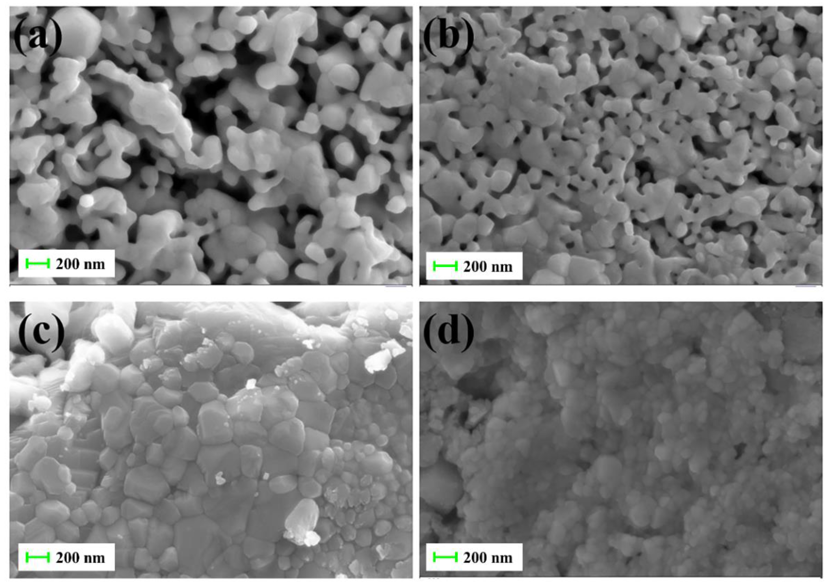
The microstructures of the sintered CCTO are shown in
Figure 3, revealing significant changes in micro-morphologies with different laser power levels. As shown in
Figure 3a the sample sintered at 25 W showed a intergranular porous structure with grain size of 50–100 nm in diameter. This indicates that the atomic diffusion and grain growth were not sufficient to form compact ceramics with subordinate laser power. When laser power increased to 45 W, the intergranular distance became smaller with denser grains. For the sample prepared at 65 W, it contained both smaller and larger grains, and some smaller grains grew into larger grains. Meanwhile, the particles started to come into closer contact and grow into compact structures. The sample prepared at 85 W showed a fine-grained, dense microstructure with an average grain size of 30 nm. This is consistent with the previous calculated grain size result from Scherrer’s formula according to X-ray diffraction patterns.
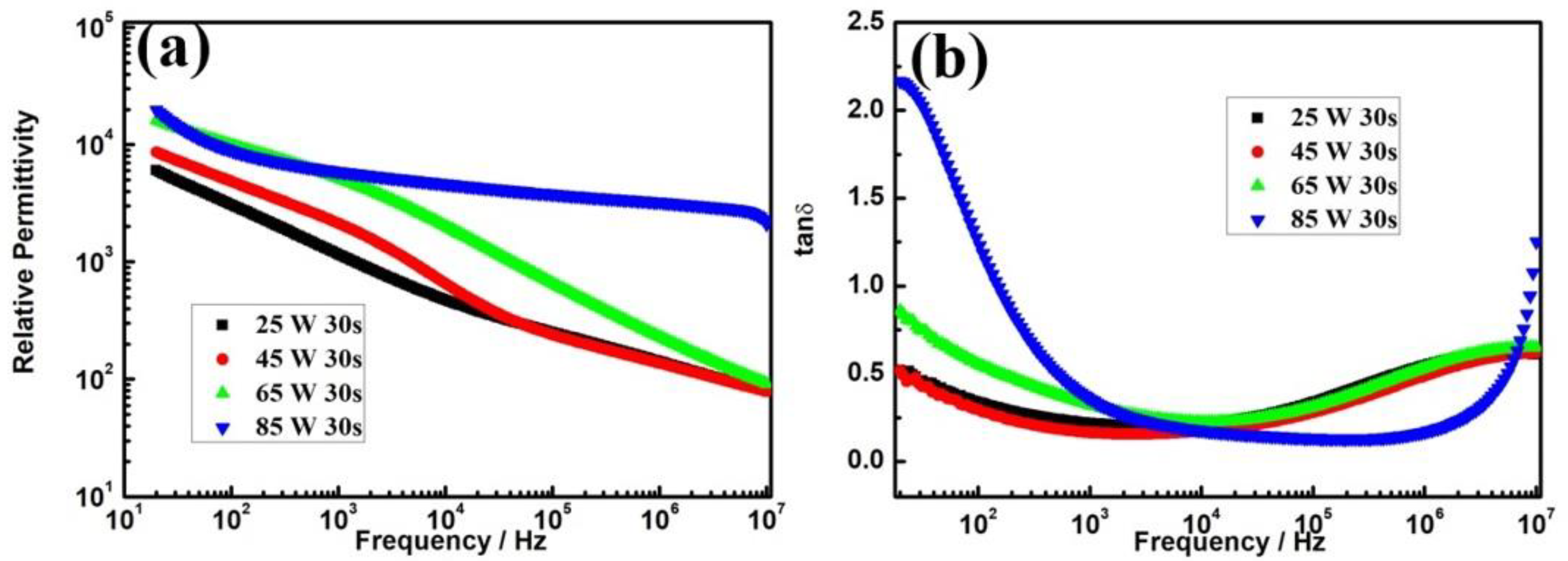
Figure 4 shows the frequency dependence of the dielectric permittivity and tan
δ of CCTO ceramics at room temperature in the frequency range of 20–10
7 Hz. All the ceramics showed high permittivity (almost more than 10
4) in the low-frequency region (
< 10
2 Hz), and the dielectric constant increased with raised laser power over the whole
range as shown in
Figure 4a. The corresponding
changed from about 10
4 to 10
2 in the range of 20–10
7 Hz for the samples synthesized at laser power of 25–65 W, showing the sharp decrease in permittivity. However, the permittivity of CCTO at 85 W experienced a slow decline from 10
5 to 10
4. It could be observed that the
maintained almost constant values in the range of 10
2–10
7 Hz, demonstrating good frequency stability. The highest permittivity value for CCTO was 10
5 at 100 Hz, and 3 × 10
3 for CCTO prepared at 25 W at 100 Hz. The reported common value of permittivity can reach 10
3 for CCTO thin films, 10
4 for poly-crystalline ceramics, and 10
5 for single-crystalline [
9,
11,
12,
19]. As per the diffraction patterns and SEM images, the CCTO sintered by laser should belong to a poly-crystalline structure. The
increased quickly with increasing laser power, which can be seen from the changes in microstructures in the SEM images shown in
Figure 3. The denser microstructures had a higher dielectric permittivity than those of a looser structure. When exceeding 10
5 Hz, the relationship curves of permittivity vs. frequency for the samples under 65 W linearly declined, which could be ascribed to the well-known Debye-like relaxation [
19,
24]. As a result, the frequency stability should be closely connected with the grain size, density of grain boundaries, and the compactness of ceramics. In addition, the laser power should be regulated for a suitable value to synthesize purer CCTO, and the arbitrary power increase will lead to the appearance of impurities such as oxygen vacancies in CCTO.
Figure 4b shows the frequency dependence of dielectric loss (tan
δ) at room temperature. It can be seen that the tan
δ of CCTO ceramics declined from a low frequency to a platform in middle frequency and then gently increased at high frequency. In the low-frequency range of 20–10
2 Hz, tan
δ decreased slowly for all the samples with increasing laser power, which can be attributed to the direct current (dc) conduction effect in the bulk [
25]. Singh et al. [
26] studied the CCTO-based nano-composite by the conventional solid-state synthesis method and concluded that the higher
and loss at the low
may be ascribed to the appearance of interfacial space charge polarization. In addition, it is interesting that the samples sintered at low power had lower loss with low permittivity, while the sample sintered at 85 W had slightly higher dielectric loss in the low-frequency region. The dielectric losses for CCTO sintered at 25 W, 45 W, and 65 W were less than 0.8 in the whole frequency range of 20–10
7 Hz, due to the contribution of micro-structural defects such as pores, valence diversity, and oxygen vacancies [
24]. The dielectric loss also was sensitive to the micro-morphologies, which could be seen by comparison of the SEM images at different laser power rates. It should be noted that the sintered sample at 85 W exhibited lower dielectric loss (~0.1) in a wide frequency range of 10
3–10
6 Hz, indicating that CCTO materials by laser sintering show more competitiveness for potential applications. Thus, it can be deduced that a compact structure composed of a number of smaller grains could aid in the improvement of overall dielectric performance.
Figure 5 shows the dielectric permittivity and loss of CCTO sintered at 85 W with temperature at some fixed frequencies. The dielectric permittivity obviously increased with raised temperature and decreased with increasing frequency. However, in higher temperature regions (>250 °C), the dielectric behavior changed at a different frequency, presenting a flat platform of 2.1 × 10
4, 1.8 × 10
4, and 1.6 × 10
4 of dielectric permittivity at 1 kHz, 5 kHz, and 10 kHz, respectively. At 1 kHz the permittivity was 22,000 in the range of 200 °C–250 °C, which was the highest value. The decrease in dielectric permittivity at higher frequencies can be explained in terms of the interfacial space charge polarization, which is due to heterogeneous microstructures. The space charge polarization will be enhanced at higher temperature due to the increasing dc conductivity. As a result, the interfacial polarization has a rapid increase in permittivity at high temperatures and low frequencies [
25].
Figure 5b shows the changes in tan
δ with temperature at fixed frequencies. It could be seen that the tan
δ demonstrated a trend of firstly increasing, then decreasing, and finally increasing with rising temperature for all given frequencies. Basically, the tan
δ was lower at higher frequency due to the increase in the conductivity with rising temperature, except for relaxation peaks. With increasing frequency, the location of the relaxation peaks shifted to the high-temperature region. The dielectric loss of CCTO-based ceramic materials was strongly temperature-dependent and the clear relaxation peaks could be due to the thermally activated relaxation.
Figure 6 shows the variation of the real part of the impedance with frequencies at different temperatures for CCTO sintered at laser power rates of 25 W, 45 W, 65 W, and 85 W, respectively. The values of Z’ decreased with increasing temperature below 10
5 Hz for all the samples, and then the Z’ values almost merged at high frequency for the range of 10
5–10
7 Hz. The different Z’ values indicate the various electrical properties related the microstructures, leading to the dependence of Z’ on frequencies. For the CCTO sintered at 25 W and 45 W, the Z’ values diverged more than the samples sintered at higher power. Some reports attribute this dispersion at a lower frequency to the release of space charge polarization with increasing temperature and frequency, which may be associated with charge carrier hopping between para-electric phase [
27,
28]. However, this does not explain the merging at higher frequencies, which may have same main factor for the dependence of Z’ on frequency. We found that for the same CCTO materials with different synthesis methods, the dispersion at low frequency had different frequency ranges. It would be interesting to further ascertain the mechanisms of the different dispersion phenomena.
Figure 7 shows the complex impedance spectra (Z’’ versus Z’, Nyquist plot) of CCTO ceramics sintered at various laser power rates with the measured temperatures of 25–300 °C. Impedance spectra measurement is powerful tool which can clarify the working mechanism of the microstructure and interface as well as the total electrical conduction behavior of polycrystalline materials by using the simplest equivalent RC circuit model [
29,
30]. In general, impedance plots are composed of two semicircular arcs with an intercept on one real axis corresponding to the grain resistance (
Rg) and on the other for the grain boundary resistance (
Rgb) [
2]. It can be seen from
Figure 7 that the experimental impedance data only show a part of the arcs because of the limit of the measured range, indicating a fraction of the grain boundary arc is detected in the CCTO ceramics. The inset of
Figure 7a shows an equivalent circuit which includes two parallel RC elements connected in series. The frequency dependent impedance plots can be modeled as weak semicircular and clear semicircular curves for grain and grain boundaries, respectively. It can be observed from
Figure 7 that the resistance values of the grain and grain boundaries decrease with rising laser power, which can be explained as follows: at low laser power, the CCTO ceramics have some porosity and low compactness, and a decrease in porosity and increase in grain growth simultaneously occur with increasing laser power. The laser power influences the CCTO bulk (
Rg) and its grain boundary (
Rgb). Moreover, the diameter of semicircle reduces with the rising temperature, revealing that the resistance of all the CCTO ceramics demonstrates a negative temperature coefficient [
29]. Based on the equivalent circuit, the values of the
Rg and
Rgb were fitted and obtained using Z-View software, as shown in
Table 1.
To reveal the key role of grain boundaries in CCTO performance, the effect of temperature on conductivity of grain boundary was investigated, and the resistance of grain boundary (
Rgb) was deduced from the impedance spectra as described in
Table 1. According to the Arrhenius equation, the electrical conductivity is strongly dependent on temperature, which can be written as:
where
is the pre-exponential factor,
represents the activation energy of the grain boundary,
is the Boltzmann constant, and
T is the absolute temperature, respectively.
Figure 8 shows the plot of ln
vs. 1/
T, in which the solid lines show the results fitted using Arrhenius equation for CCTO ceramics sintered at different laser power rates. The experimental data obeys the equation approximately. The calculated activation energy of grain boundaries
can be deduced: 0.601 eV, 0.628 eV, 0.633 eV, and 0.532 eV for CCTO sintered at 25 W, 45 W, 65 W, and 85 W, respectively. The magnitude of
is close to the reported values from a similar analysis of CCTO-based ceramic materials, where an activation energy between 0.5 and 0.7 eV was obtained. The
value of 0.532 eV in the sample sintered at 85 W suggests the modification of electrical conductivity of grain boundaries, which is due to the increase of charge carrier motion at the grain boundaries.


