Article

Directly Printed Hollow Connectors for Microfluidic Interconnection with UV-Assisted Coaxial 3D Printing

by
Qianwen Xu
1,2,
Jeffery Chi Chuen Lo
2,3 and
Shi-Wei Ricky Lee
1,2,3,4,*
1
Department of Mechanical and Aerospace Engineering, The Hong Kong University of Science and Technology, Hong Kong 999077, China
2
Electronic Packaging Laboratory, The Hong Kong University of Science and Technology, Hong Kong 999077, China
3
HKUST Foshan Research Institute for Smart Manufacturing, The Hong Kong University of Science and Technology, Hong Kong 999077, China
4
HKUST LED-FPD Technology R&D Center at Foshan, Foshan 528200, Guangdong, China
*
Author to whom correspondence should be addressed.
Appl. Sci. 2020, 10(10), 3384; https://doi.org/10.3390/app10103384
Submission received: 31 March 2020 / Revised: 7 May 2020 / Accepted: 9 May 2020 / Published: 14 May 2020
(This article belongs to the Special Issue Advances in 3D Printing for Miniaturized Instruments)

Abstract

:
Effective and reliable interconnections are crucial for microfluidics to connect with the macro world. Current microfluidic interfaces are still bulky, expensive, or with issues of clogging and material limitation. In this study, a novel ultraviolet (UV)-assisted coaxial three-dimensional (3D) printing approach was proposed to fabricate hollow microfluidic connectors with advantages of rapid prototyping, fixture-free, and materials compatible. An assembled coaxial nozzle was designed to enable co-flow extrusion, where the inner flow (water) served as the sacrificial layer and the outer flow (adhesive) was cured for shell formation. Furthermore, a converged UV-LED light source was attached to the coaxial nozzle for UV curing of adhesives. UV rheological characterizations were performed to study the UV curing kinematics, and the gelation time was employed to describe the state transition behaviors of UV curable adhesives used in the study. To explore requirements for successful hollow connectors direct printing, processing criteria such as co-flow regime and pre-cure time were investigated. The hollow connectors with an inner channel diameter of ~150 μ m and a height of 5 mm were successfully printed on polymethyl methacrylate (PMMA) and glass substrate. The integration feasibility of the proposed method was also demonstrated by the presented microfluidic device with printed hollow connectors.

1. Introduction

The emergence of micro-electromechanical systems (MEMS) was regarded as the most significant milestone in the last century. By integrating electronic and mechanical elements such as sensors and actuators on a common substrate with advanced microfabrication capabilities, MEMS can provide us with ever smarter, smaller and cheaper devices [1]. As one type of MEMS, microfluidics refers to the fluids’ manipulating technology based on channels with a dimension of tens to hundreds of micrometers [2]. Compared with traditional fluid handling technology, microfluidics can miniaturize the device sizes, reduce the reagent amounts, and achieve high sensitivity. Besides, the scale-dependence of fluid behaviors in microfluidics can bring numerous application opportunities [3]. Over the past decades, microfluidics has spread widely to chemical, biological, and biomedical research areas and related industries. However, effective and reliable interconnections between microfluidics and the macro world are still the technical challenges for its continuing development. To realize a stable world-to-chip interface, ideal fluidic interconnection should meet the following requirements: minimal dead volume, easiness of plugging/unplugging, reliability at high pressures, low-cost and straightforward techniques, and compatibility with commercial tubes and fittings [4].
Due to various materials and fabrication techniques for microfluidic chips, there are different interfacing solutions specific to the target applications [5]. The earliest materials introduced to microfluidic manufacturing are silicon and glass [6]. Benefiting from mature microfabrication technology, complex and precise microchannel networks could be easily defined. Deep reactive ion etching (DRIE) interlocking structures [7,8] have been reported for the interconnections of silicon-based microfluidic devices. They are reversible, adhesive-free, geometric versatile, enabling high density but expensive. Silicon-based microfluidic devices provide well-characterized surface properties and high qualities. Nevertheless, they are not as attractive as polydimethylsiloxane (PDMS)-based and thermoplastic-based microfluidic devices because of the high cost [9]. With the emerging of PDMS in the early 2000s [10], the straightforward fluidic interconnects for PDMS-based microfluidic devices were developed. Commercial tubing or needle could be directly inserted into holes punched on PDMS by compression sealing [11,12]. They are easy to plug/unplug, adhesive-free, reversible, and compatible with moderate pressures. PDMS is an excellent material for rapid prototyping and simplified world-to-chip interfaces. However, it still has drawbacks such as short-term stability after surface treatments, swelling in organic solvents, water permeability, and incompatibility with very high pressures [13]. Besides, PDMS is not the right choice for large scale production due to molding and curing processes. Thermoplastic and paper were preferred as low-cost, robust, and mass-producible alternatives in microfluidic industries [14,15]. New approaches were proposed for thermoplastic-based microfluidic devices. For example, ultrasonically welded connectors were demonstrated in recent years [16,17]. They are mechanically stable, capable of rapid implementation and large-scale production but face risks of clogging.
Additionally, there are some packaging strategies compatible with different materials. One of the most common methods is adhesives-based gluing [18,19]. It can enhance the robustness and reliability of fluidic connections. The main challenge of using adhesives is the clogging to the connecting tubing and microfluidic channels. Another type is the designed fixtures or frames for applying a significant compression force to ensure a leak-free connection. Press-fit interconnects [20,21,22], screw fittings [23], vacuum fixtures [24], and magnetic connectors [25,26] have been developed. They are adhesive-free, reversible, reliable at high pressures but hard to be miniaturized or integrated. Alternatively, additive manufacturing (AM) offers more flexibility and benefits for the microfluidic designs and its fabrication [27,28,29]. For instance, sophisticated structures (e.g., three dimensional) over traditional planar microfluidic chips could be easily implemented with AM technique. Moreover, the potential for monolithic construction of 3D printed microfluidic devices [30,31] could significantly improve the process yield and decrease the manufacturing time and costs, while eliminating photo-lithography, bonding, molding process, etc. In addition, fluidic ports can be fabricated in the monolithic 3D printing process to serve as the world-to-chip interface for 3D printed microfluidic devices. Nevertheless, for monolithic 3D printed microfluidic devices, the high resolution and smaller features rely on the material properties of photosensitive resins and the pixel sizes of UV light source. Currently, silicon, glass, PDMS, paper, and thermoplastic are still commonly used materials for microfluidic devices specific to target applications (e.g., thermoplastic microfluidic devices for low-cost and commercial products). Directly printed connectors proposed in the study can provide a general connector solution to an existing microfluidic device.
In this paper, a novel approach for microfluidic connectors direct printing was proposed based on a UV-assisted coaxial 3D printing system. To fabricate hollow connectors with channels at a micro-scale, water served as the sacrificial layer to avoid channel collapsing. At the same time, UV-curable adhesive was utilized for shell formation under UV radiation. Table 1 represents the comparison between current microfluidic interface solutions and the proposed approach from different aspects. The proposed approach of directly printed connectors is rapid prototyping, material-compatible, fixture-free, easy to plug/unplug, leak-free, and non-clogging. Section 2 describes the materials used in the study, the design of the UV-assisted coaxial 3D printing system for directly printed connectors fabrication, and the fabrication process of PDMS-Glass microfluidic devices with printed connectors for functionality demonstration. Section 3 reports the experiment results: (1) UV rheological characterizations for material conversion; (2) co-flow behaviors in the co-flow system; and (3) processing criteria (co-flow behavior regime and pre-cure time) for successful hollow connectors printing. Besides, the functionality and integration feasibility of directly printed connectors are exhibited and discussed in Section 3. Section 4 summarizes the work and proposes directions for future research.

2. Materials and Methods

2.1. Materials

In the study, UV curable adhesive (LOCTITE 3491, Henkel AG & Company, Düsseldorf, Germany) was selected for printing materials to enable simple and rapid fabrication together with excellent adhesion performance. PMMA and glass were chosen for printing substrate materials, which are commonly used for microfluidic fabrication. Photoresist (PR) AZ4620 (AZ Electronic Materials, Luxembourg) and developer FHD-5 (FUJIFILM Electronic Materials Co., Ltd, Tokyo, Japan) were utilized for silicon master mold fabrication. Trichloro (1H,1H,2H,2H-perfluorooctyl) silane 97% (Sigma-Aldrich, St. Louis, MO, USA) was used for hydrophobic modification of silicon master mold surface. PDMS, SYLGARD 184, was purchased from Dow Corning Corporation, Midland, Michigan, USA. Inks with different colors were added to water to distinguish it from the transparent adhesives and to trace the liquids flowing in the presented PDMS–Glass microfluidic device. Silicone was selected for transparent jacket material for pre-cured adhesives extrusion due to its hydrophobic property.

2.2. UV-Assisted Coaxial 3D Printing System

A UV-assisted coaxial 3D printing system is shown in Figure 1a. A commercial dispenser (PACHDA, Shenzhen, China) served for the 3D movement stage with an xy axis moving plate and one robot arm at the z–axis. The extruder part of the original dispenser was replaced by an assembled coaxial nozzle with two syringe drivers. The assembled coaxial nozzle consisted of a 28 G (inner diameter, ID, 0.17 mm; outer diameter, OD, 0.35 mm) inner steel needle for water, an 18 G (ID 0.91 mm, OD 1.26 mm) outer steel needle for UV adhesive and other accessories. A transparent jacket (ID 1 mm, OD 2 mm) with a length of 25 mm was attached to the outer needle for the pre-curing of materials. Figure 1b represents the bottom view of the assembled coaxial nozzle for clarification. Fluids were fed through syringes to the coaxial nozzle by Luer tapers. Syringe drivers with stepper motor could quantitatively control the flow rates of both fluids. Moreover, a converged UV-LED light source attached to the coaxial nozzle was designed for UV curing. Two UV LEDs with a power of 3 W at 365 nm were placed on each side for more uniform radiation. With the assistance of the transparent jacket attached to the coaxial nozzle, UV adhesive was able to be pre-cured before its deposition to stabilize the structure. During the printing process, the inner flow (water) was selected as the sacrificial layer, while the outer flow (UV adhesive) was cured for shell formation under UV radiation. As the coaxial nozzle moved upwards, vertical hollow connectors could be directly printed on the substrate with matching holes. Finally, the printed connectors on the substrate was illuminated by a UV mercury lamp with high power to fully cure.
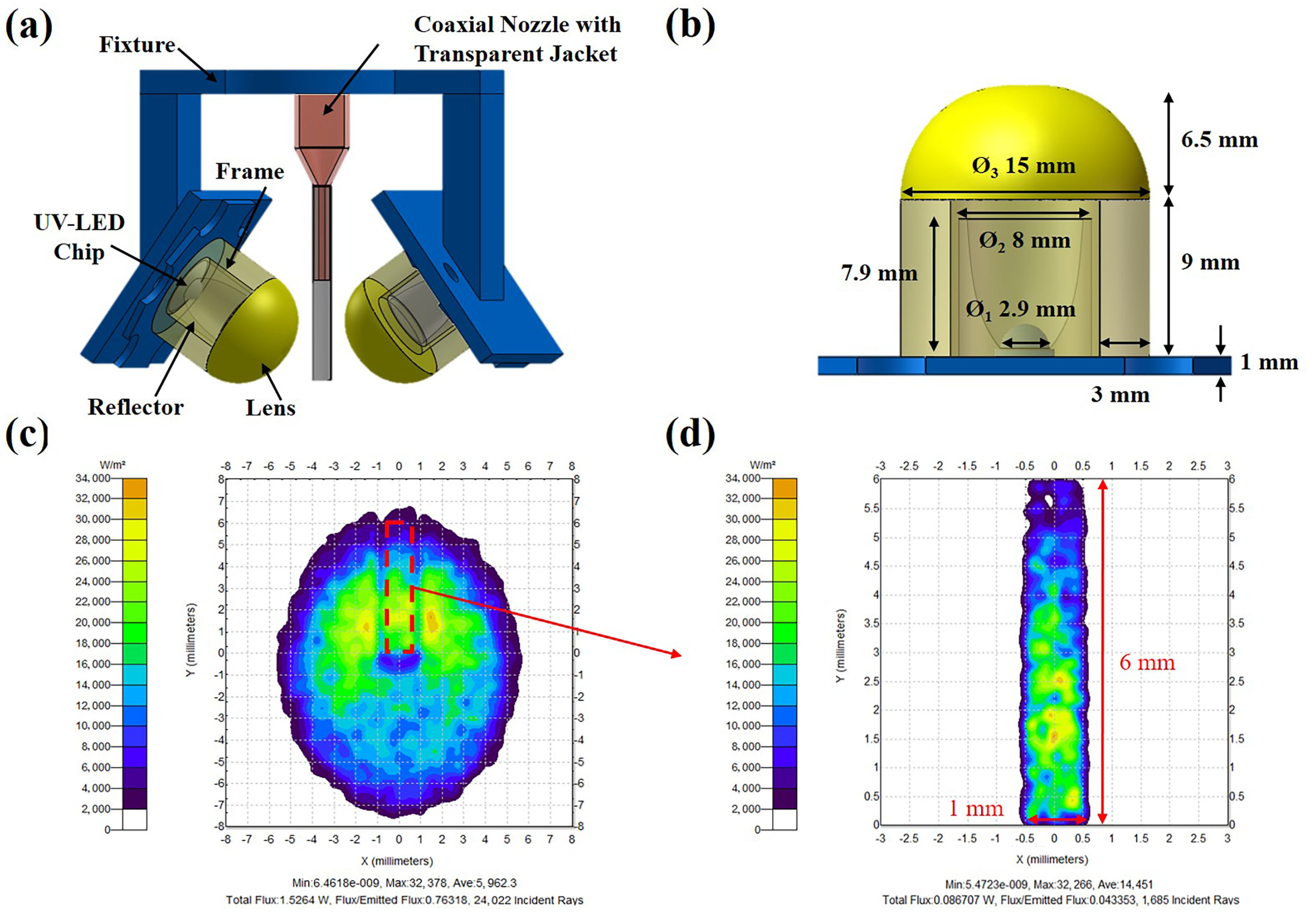
According to preliminary experiments conducted, a UV light source with the requirements of a large radiation area with uniform flux was suitable for the direct hollow connector printing process. Thus, a converged UV-LED light source was designed. Figure 2a schematically describes its design. UV light emitted from the chips at 365 nm on each side could be converged through packaged aluminum reflectors and glass lenses. Dimensions of the converged UV LED were clarified in Figure 2b. The UV-LED chip of purchased products (UV Z5 series, Seoul Viosys, Korea) had an irradiation area of 1.4 × 1.4 mm 2 with the maximum radiant flux of 1 W. The chip was encapsulated by silicone resin with a hemispherical shape (radius, 1.45 mm). For electrical connection, the chip was bonded to an aluminum substrate (thickness, 1 mm) with solder pads. The aluminum reflector was in a cone shape (Ø 1 2.9 and Ø 2 8 mm) with a height of 7.9 mm. The diameter and height of the glass lens were 15 and 6.5 mm, respectively. A cylindrical plastic frame (Ø 3 15 mm, height of 9 mm, and thickness of 3 mm) was used for packaging the converged UV-LED. In Tracepro ray-tracing, each UV LED radiation flux was set to 1 watt with Lambertian angular distribution. The input parameters of material optical characteristics are listed in Table 2. The refractive index (RI) and the absorption coefficient of glass at 365 nm are 1.54 and 0.001 mm 1 , respectively; the RI and absorption coefficient of aluminum at 365 nm are 0.40 and 1.52 × 10 5 mm 1 , respectively; and the RI and absorption coefficient of silicone at 365 nm are 1.54 and 0.12 mm 1 , respectively. According to the mechanical design and material optical properties, UV radiation area and intensity at the vertical middle plane were simulated by Tracepro ray-tracing. As shown in Figure 2c, the total UV radiation area is in ellipse shape with a length and width of around 13 and 10 mm, respectively. The UV radiation part distinguished by the red rectangles is the UV radiation for the bottom part of the transparent jacket. Adhesives could be pre-cured to stabilize its structure when passed through the bottom part of the transparent jacket. The UV intensity for pre-curing was estimated to an average of 1.45 W/ cm 2 with an area of 1 × 6 mm 2 (Figure 2d).

2.3. Fabrication of PDMS–Glass Microfluidic Device

The PDMS–Glass microfluidic devices with proposed printed connectors were fabricated by soft lithography process [32,33], as shown in Figure 3. Firstly, the silicon wafer was coated by photoresist (AZ4620) with a thickness of 7 μ m. After the photolithography (SUSS Microtec MA6, Garching, Germany) and development (FHD-5), the micro-channels layout was patterned on the silicon wafer. Secondly, the micro-channels pattern at a depth of 100 μ m was etched by the DRIE process. With PR stripping, the silicon wafer could serve as the master mold for PDMS casting. To release the PDMS replica from the mold easily, the surface of the silicon master mold should be hydrophobically modified by the FAS (Fluoroalkylsilane) coating. Therefore, the silicon master mold was put in a vacuum chamber with 100 μ L of Trichloro (1H,1H,2H,2H-perfluorooctyl) silane 97% for 2 h for surface treatment. Thirdly, a PDMS mixture was prepared with a monomer and curing agent at a ratio of 10 to 1. After mixing and degassing (Mazerustar ® planetary mixer, Technic Inc., Cranston, RI, USA), the PDMS mixture was poured on the silicon master mold and then cured on a hot plate at 80 °C for 2 h. After that, the cured PDMS layer could be peeled off from the mold and cut into individual pieces. The last step was the PDMS–Glass microfluidic chip assembly. At first, hollow connectors were directly printed on the glass slide with matching holes (Ø 2.5 mm) in advance. The target length of printed connectors was set to 5 mm for sufficient sealing performance, as referred to the typical design of reported microfluidic connectors [8,17]. Then, the glass slide with printed connectors was bonded with an individual PDMS piece by plasma treatments. In detail, bonding surfaces of the glass slide and the PDMS piece were exposed in oxygen plasma for 90 s and then aligned and contacted under a microscope. Finally, the assembled PDMS–Glass device was put on the hot plate at 80 °C for 1 h for bonding strengthening. Through commercial silicone tubes fitted on the printed connectors by compression sealing, PDMS–Glass microfluidic chips could be connected with the macro world for liquid/gas passage.

3. Results and Discussion

3.1. UV Rheological Characterization

To characterize the solidification behaviors of the adhesive under UV exposure, rheological measurements were evaluated by a rheometer (Discovery HR-2, TA Instruments, New Castle, PA, USA) equipped with UV curing accessories. Omnicure S2000 model (Excelitas Technologies Corp., Waltham, MA, USA) was used for UV light source with a wavelength of 365 nm. A plate-to-plate geometry with a diameter of 20 mm was selected to place the liquid sample in the gap between two plates. The gap was set to 800 μ m in all measurements. With torques applied, the rheological properties of samples could be measured. The initial viscosity of LOCTITE 3491 was measured under variable shear rates. It was observed that LOCTITE 3491 can be categorized into the Newtonian liquid with shear rate independent behavior. The value of the initial viscosity was 0.95 Pa·s. The initial storage modulus and loss modulus were 1.50 and 9.70 Pa, respectively. Thus, in all rheological measurements, the angular frequency and strain were set to 10 rad/s and 1% constantly.
Figure 4a describes the UV rheological results of material viscosity under UV exposure of 1 W/ cm 2 at 365 nm. As UV exposure time increased, the material was cured rapidly whereas the viscosity grew sharply until it reached several orders larger than the initial value after 15 s. Figure 4b illustrates the moduli variation under the same UV exposure. In rheology, shear modulus is used to describe the viscoelastic behavior of samples, in which the storage modulus G’ represents the elastic portion (solid-state behavior) and the loss modulus G” characterizes the viscous portion (liquid-state behavior) [34]. In the modulus measurements, initially, G’ was lower than G”, indicating the liquid-like behavior. As UV irradiation continued, G’ and G” were both overgrowing. G’ crossed over G” and became larger than G”, representing the solid-state behavior. The gelation point is defined as the cross over point of the storage modulus and loss modulus where the material is transferred to a gelation-like structure. Furthermore, gelation time (GT) is defined as the time material reaches its gelation point.
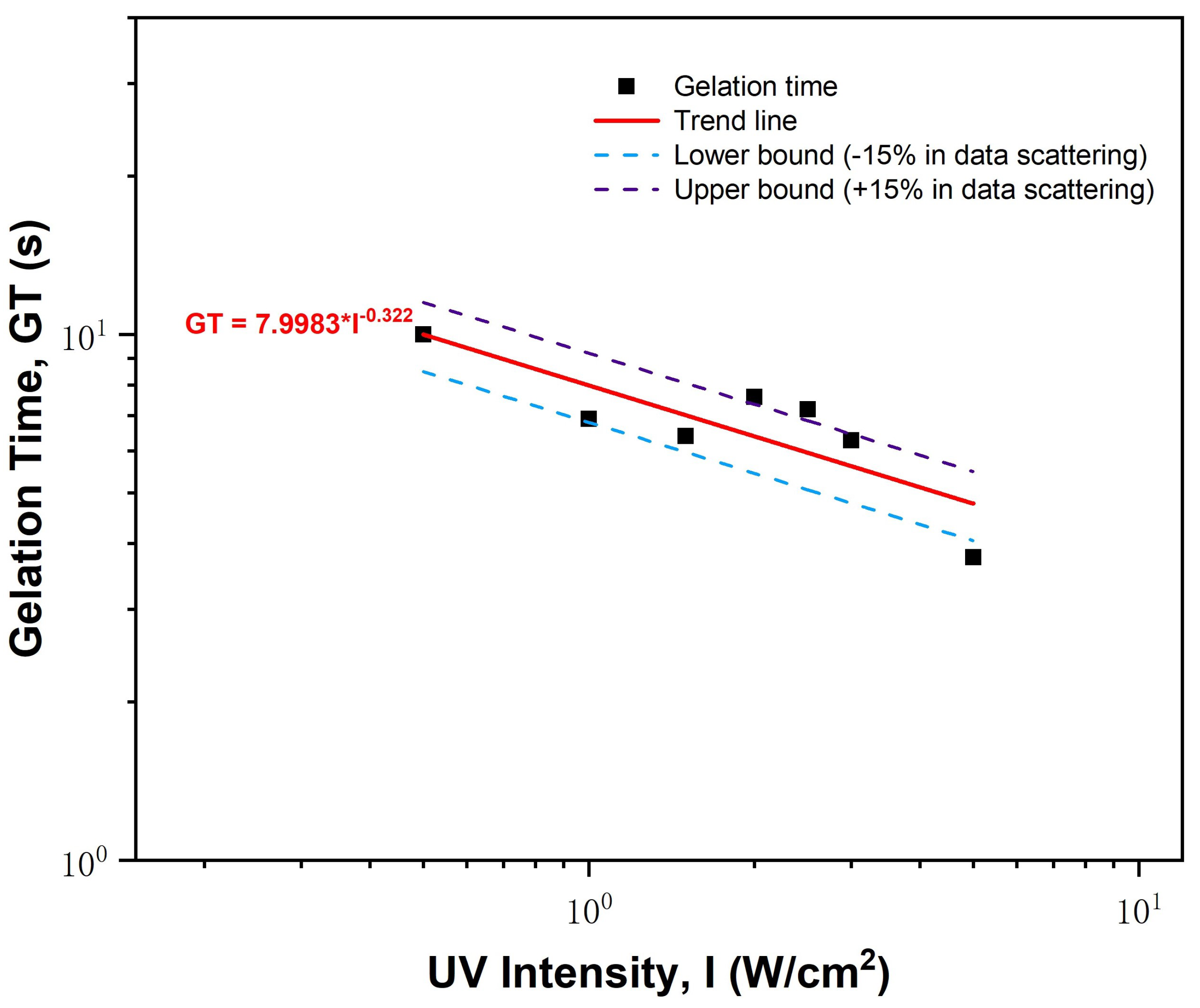
To further characterize the effect of UV intensity (I) on rheological results, the UV curable adhesive was exposed to different UV irradiation with varying intensities. Generally speaking, for all intensities investigated, they showed similarities in the material solution/gelation transition. However, higher UV intensity represented the tendency to accelerate the UV curing reaction. Table 3 summarizes the value of gelation time under different UV intensity from 0.5 to 5.0 W/ cm 2 . As shown in Figure 5, the relationship between the gelation time and UV intensity was data fitted ( G T = 7.9983 × I 0.322 ) and showed a power-law dependence, which is consistent with previous works [34,35]. Moreover, a sensitivity analysis on the effect of the data scattering on curve fitting has been performed to find the upper/lower bound for gelation time predication with an assumption of ±15% in data scattering. Gelation time could be employed to predicate the cross-linking status of materials in UV-assisted coaxial 3D printing. According to Tracepro ray-tracing, the UV intensity for the pre-curing of UV adhesives is simulated to an average of 1.45 W/ cm 2 . Based on the fitted relationship between gelation time and UV intensity (GT∼ I 0.322 ), the calculated gelation time for 1.45 W/ cm 2 intensity is 7 s. Furthermore, with the assumption of ±15% in data scattering, the upper/lower bound of the estimated gelation time for 1.45 W/ cm 2 intensity is 7 s ± 1 s.

3.2. Co-Flow Criterion for Printing Process

As illustrated in the proposed approach, an assembled coaxial nozzle was designed to enable the co-flow extrusion, whereas water was used as the sacrificial layer, and the UV curable adhesive was used as the outer fluid for shell formation. Because the two liquids were immiscible with each other, the core liquid could present a continuous jetting or dripping (pinching off to droplets) behavior while flowing together [36,37,38]. Many relevant parameters influence the co-flow regimes such as viscosity, fluid density, flow rate, channel dimension, and the interfacial tension. Under the specific coaxial nozzle design and two selected fluids, flow rates were the significant controllable parameters which determine the co-flow regimes in the system.
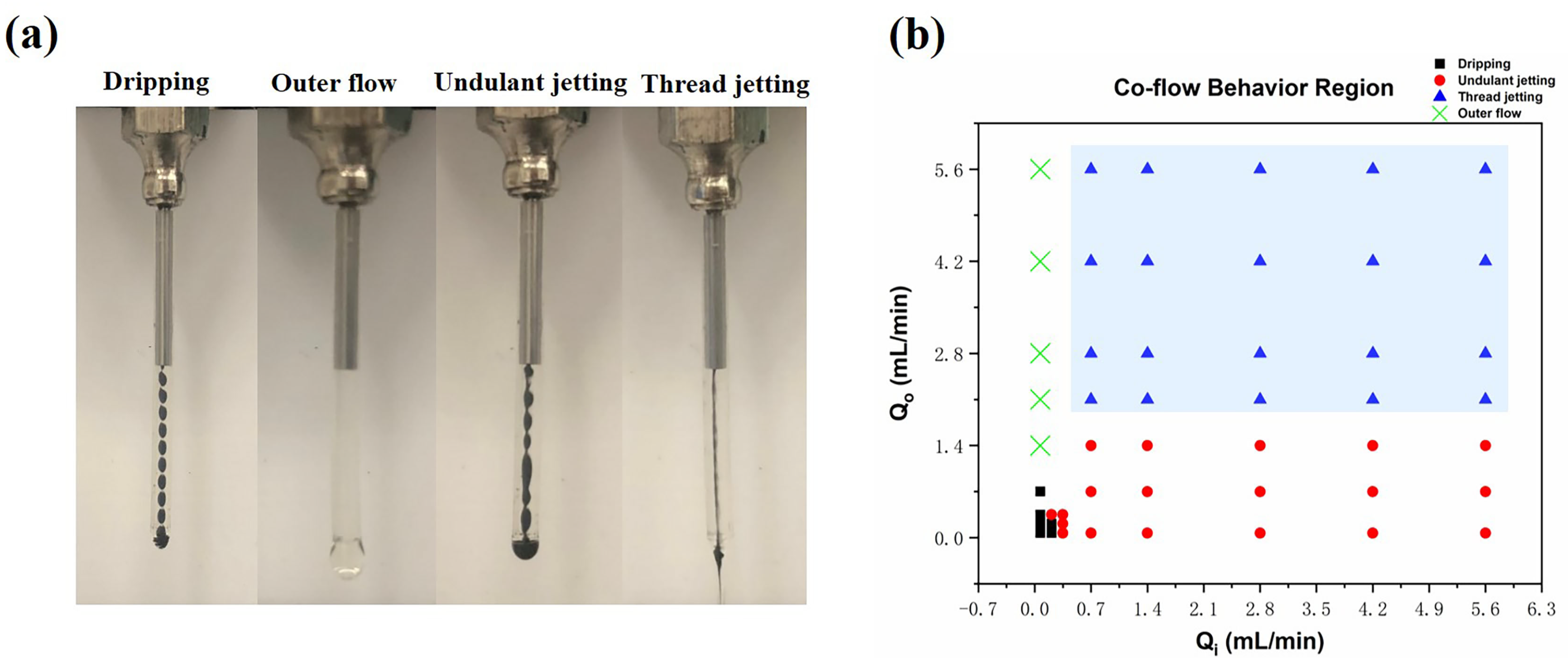
Different co-flow behavior regimes were observed with varying inner and outer flow rates Q i and Q o . The inner flow (water) was marked with black ink to distinguish it from the transparent adhesive. Figure 6a represents four kinds of typical co-flow behavior regime including dripping, outer flow, undulant jetting, and thread jetting. As both Q i and Q o were small, inner flow (water) would pinch off to droplets, result in dripping. When increasing Q o under small Q i , the co-flow behavior would be changed to outer flow, in which the inner flow could not be extruded out due to the high external pressure. When increasing Q i under small Q o , the co-flow behavior regime would be transferred to undulant jetting with the inner fluids of flow instability. When increasing Q i and Q o simultaneously, the inner flow (water) would be well constrained to thread-like flowing status by the external pressure, which is described as thread jetting. Co-flow behavior regimes were parametric investigated, which covers the flow rate range of 0.07–5.6 mL/min for both Q i and Q o . Figure 6b concludes the co-flow behavior region and thread jetting were distinguished with a blue shadow. To fabricate hollow connectors with a continuous and uniform channel, the thread-jetting regime was chosen for the co-flow criterion for the hollow connectors direct printing process.

3.3. Pre-Curing Criterion for Printing Process

Material conversion from liquid to solid state is crucial in the hollow connectors direct printing process. Not only does material conversion relate to intrinsic material properties, but it is also influenced by processing-related parameters such as UV intensity, exposure length, extrusion and printing speed. According to UV radiation simulations and rheological characterizations, the adhesive chosen in the study was predicted to reach the solid-like state with a gelation time of 7 ± 1 s during the printing process. Thus, it was proposed that the material was pre-cured to solidification before the deposition to succeed in hollow connectors printing. Figure 7a schematically describes the material conversion mechanism during the process. Two fluids were extruded out from the tip of the coaxial nozzle and then pass through the transparent jacket. UV adhesives constrained in the transparent jacket were illuminated by UV light with a length of 6 mm. The length is also called the exposure to deposition length. With enough UV exposure, materials can be converted to solid-state and then deposited. When the nozzle moving upwards, stabilized hollow structures would be printed on the substrate under a thread-jetting co-flow behavior regime.
Pre-cure time is defined here as T p . It was estimated by the exposure to deposition length dividing to the printing speed, assuming the material extrusion speed at the tip of the transparent jacket was close to zero caused by the significant friction. The curing criterion for the printing process was determined as the minimum pre-cure time required for successful printing. Certain parametric studies for the pre-cure time were performed under the flow rates Q i and Q o at 4 and 8 mL/min. The printing substrate was PMMA with matching holes (Ø 2.5 mm). Figure 7b,c shows some typical printing results. When the pre-cure time was set to 2 s, the material was still in liquid state and could not be printed on the substrate. When the pre-cure time was adjusted to 4 s, a hollow structure could be printed on the substrate but with a thinning behavior. At the same time, the bottom part of the printed connector was swelling due to insufficient UV curing. When the pre-cure time was increased to 6 s, a uniform-shaped printed connector with a well-constrained inner channel was successfully fabricated. The outer diameter of uniform-shaped printed connectors is around 1 mm, which is well restricted by the transparent jacket. All the inner channels were filled with black colored water for straightforward observation.
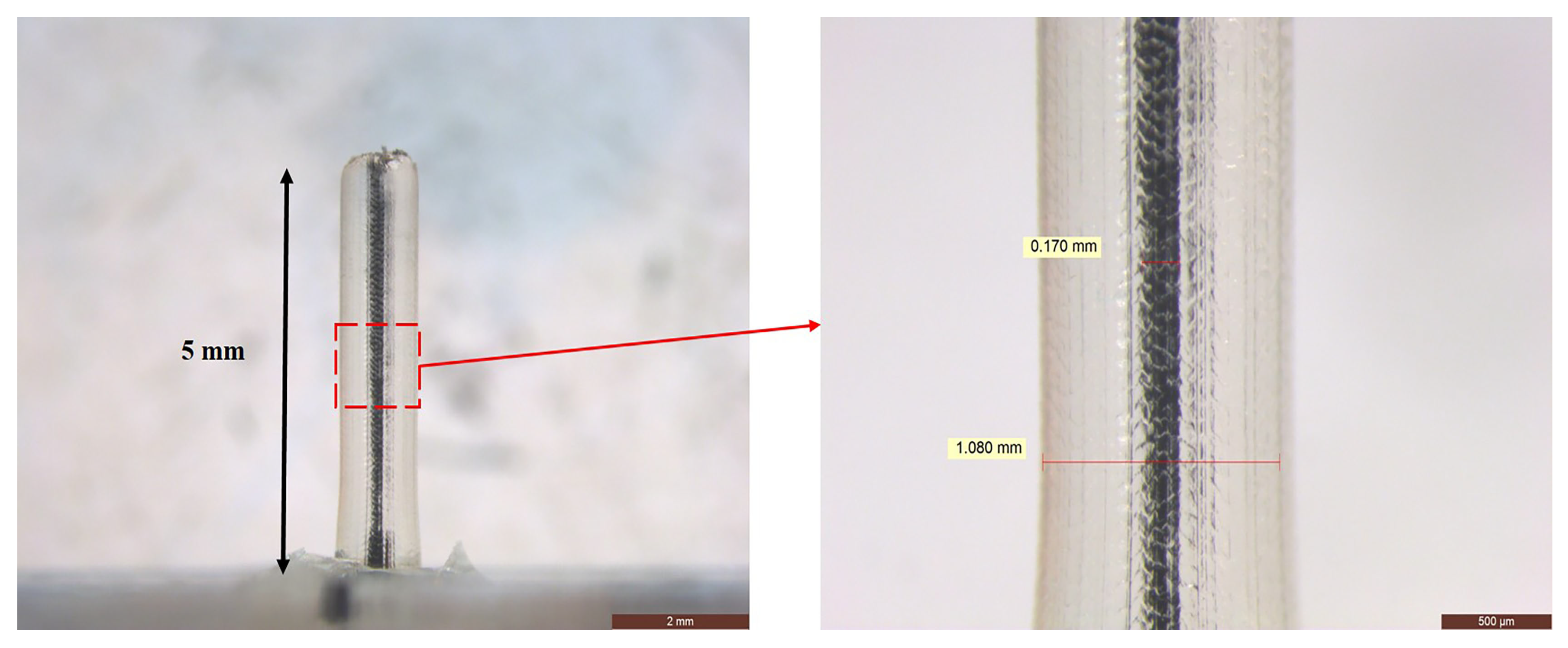
Table 4 lists the success rate of uniform-shaped hollow connectors printing with multiple printing trials of 10 times under different pre-cure time. The success rate was defined as the the times of uniform-shaped connectors (OD 1 mm) printing divided by the total printing trials under a particular pre-cure time. It was determined that the pre-cure time of 6 s was the minimum pre-curing criterion with the success rate at 100%. In addition, dimension clarification and magnified view of the successfully printed hollow connector are presented (Figure 8). The length of the printed connector was 5 mm. The inner diameter was around 170 μ m while the outer diameter was around 1 mm. The inner diameters were measured at each position with an interval of 1 mm. By standard deviation calculation, the roughness was estimated as 7 μ m. By comparing the estimated gelation time and the minimum pre-time required, gelation time was well correlated to the printing experiments.

3.4. Demonstration of Printed Connectors for Microfluidic Interconnections

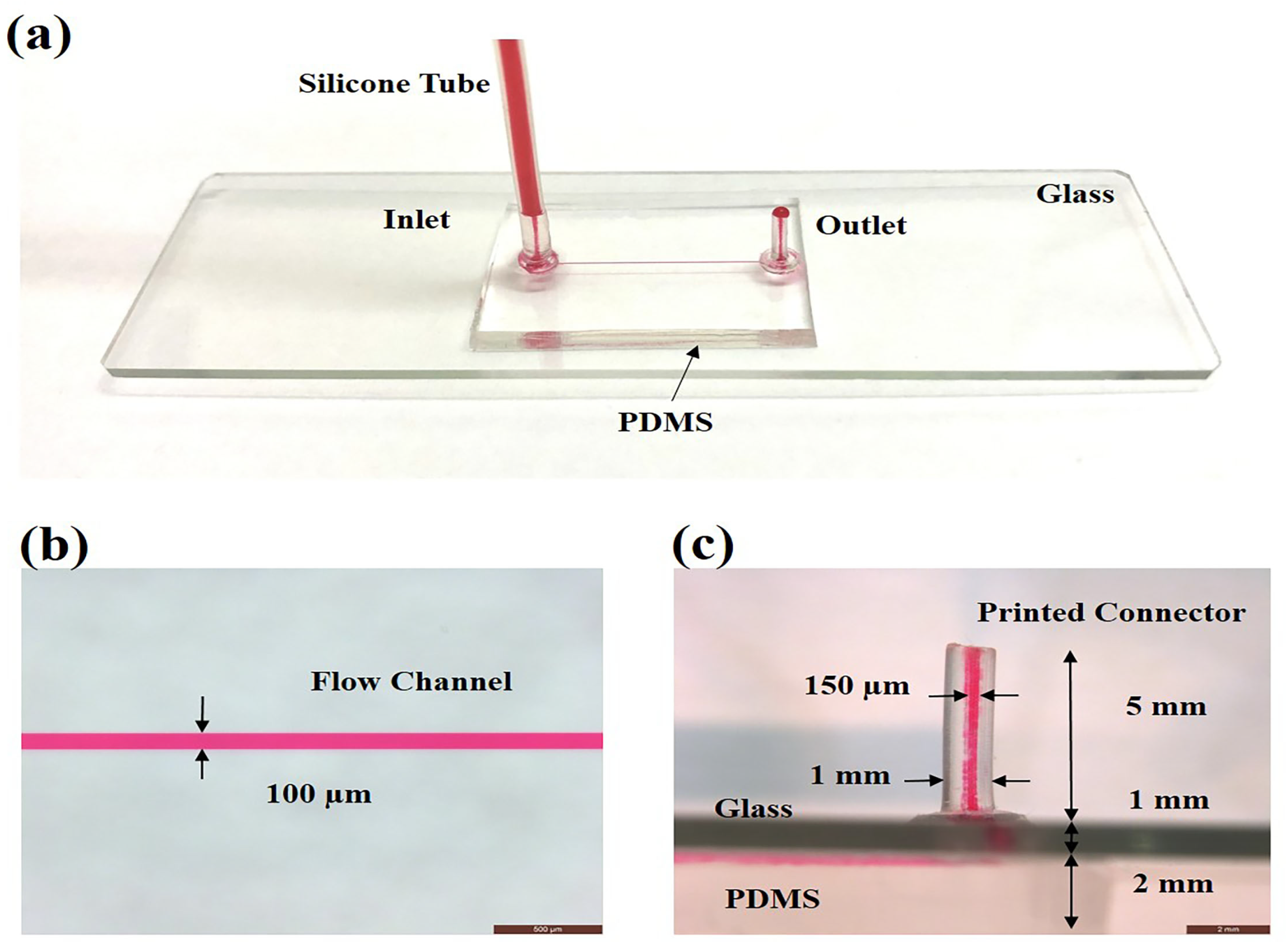
To demonstrate integration feasibilities of the proposed approach to microfluidic interconnections, a typical PDMS–Glass microfluidic device with directly printed hollow connectors was fabricated. The layout on the microfluidic device was a straight microchannel with a width and depth of 100 μ m. The microchannel was with a length of 20 mm. Alignment marks were designed on the inlet and outlet for plasma bonding. Figure 9a shows an overview of the PDMS–Glass microfluidic device. A glass slide with printed hollow connectors was bonded with the patterned PDMS piece by oxygen plasma bonding. A commercial silicone tube (ID 0.8 mm, OD 1.9 mm) was inserted to the printed hollow connectors (ID 150 μ m, OD 1 mm) on the inlet by inference fitting. For flowing testing, red-colored water was injected from the inlet through the silicone tube connected with the syringe. The result illustrates that colored water was flowing through the embedded microchannel on PDMS and then extruded from the top of printed hollow connectors on the outlet. Figure 9b represents the top view of the microfluidic device under a microscope, the flow channel was filled with red-colored water with a size of 100 μ m. Figure 9c describes the side view of the outlet in the microfluidic device. The thicknesses of glass and PDMS were 1 and 2 mm, respectively. The printed hollow connector had a height, inner diameter, and outer diameter of 5 mm, 150 μ m, and 1 mm, respectively. Therefore, directly printed connectors were successfully integrated with the PDMS–Glass microfluidic device and enabling the world-to-chip interconnections.

3.5. Discussion on Substrate Materials

The objective of the research was to develop a process that can print a hollow tube directly on a substrate (Substrate #1) with an orifice under the projection of the printed hollow tube. The printed hollow tube serves as a connector to an external tubing system for gas/fluid input. The orifice is a passage to the microchannel built in the next level substrate (Substrate #2). The essence and contribution of the research were the invention of the coaxial printing and the implementation of in-situ UV curing. The role of Substrates #1 and #2 is simply a vehicle for demonstration. Glass was chosen for Substrate #1 and PDMS was selected for Substrate #2. These are commonly used materials for microfluidic experiments. There may exist different material combinations for similar purposes. Future studies may use the printing technology developed on different substrate materials for their intended test configurations.

4. Conclusions

Microfluidic interface with external tubing is significant for microfluidics developments. In this study, an alternative approach for microfluidic connectors direct printing was proposed using a UV-assisted coaxial 3D printing system. An assembled coaxial nozzle was designed for the co-flow extrusion where the water served as the sacrificial layer and the UV adhesive was utilized for shell formation. A converged UV-LED light source was designed and simulated with Tracepro ray tracing. The estimated UV intensity for the pre-curing of adhesives was averaged to 1.45 W/ cm 2 with a length of 6 mm. To master the process, UV rheological characterizations were performed to investigate the UV curing kinematics. Gelation time was found to describe the material state transition. Moreover, the relationship between gelation time and UV intensity was investigated and showed a power-law dependence (GT∼ I 0.322 ). Thus, gelation time was selected to predicate cross-linking status during the printing process. To explore requirements for hollow connectors successful printing, processing criteria including co-flow criterion and pre-curing criterion were parametrically studied. It was found that thread jetting co-flow behavior regime and pre-cure time greater or equal to 6 s were the necessary requirements for hollow connectors direct printing. To further demonstrate the integration feasibility, printed hollow connectors were successfully assembled to a typical PDMS–Glass microfluidic device. The printed connector had a height of 5 mm with an inner channel diameter of 150 μ m. Directly 3D-printed connectors can provide a general interface solution to an existing microfluidic device. It presents the advantages of rapid prototyping, material-compatible, fixture-free, easy to plug/unplug, leak-free, and non-clogging. Future studies may exercise the printing technology developed on different substrate materials for their intended test configurations.

Supplementary Materials

Supplementary File 1

Author Contributions

Conceptualization, Q.X., J.C.C.L., and S.-W.R.L.; Data curation, Q.X.; Formal analysis, Q.X., J.C.C.L., and S.-W.R.L.; Investigation, Q.X.; Methodology, Q.X.; Project administration, J.C.C.L.; Supervision, S.-W.R.L.; Writing—original draft, Q.X.; and Writing—review and editing, J.C.C.L. and S.-W.R.L. All authors have read and agreed to the published version of the manuscript.

Funding

This research was financially supported by the Innovation and Technology Commission (Grant No. ITS/006/18) from the Government of the Hong Kong Special Administrative Region. This study was also supported by the HKUST Special Fund of Foshan (Grant No. FSUST19-FYTRI11).

Acknowledgments

The authors are grateful to the Nanosystem Fabrication Facility (NFF) and Yao Laboratory at HKUST for the assistance of microfluidics fabrication. Additionally, the authors would also like to extend their gratitude to the Materials Characterization and Preparation Facility (MCPF) at HKUST and HKUST LED-FPD Technology R&D Center at Foshan for material characterizations.

Conflicts of Interest

The authors declare no conflict of interest.

References

  1. Atencia, J.; Beebe, D.J. Controlled microfluidic interfaces. Nature 2005, 437, 648–655. [Google Scholar] [CrossRef]
  2. Whitesides, G.M. The origins and the future of microfluidics. Nature 2006, 442, 368–373. [Google Scholar] [CrossRef]
  3. Convery, N.; Gadegaard, N. 30 years of microfluidics. Micro Nano Eng. 2019, 2, 76–91. [Google Scholar] [CrossRef]
  4. Song, I.H.; Park, T. Connector-Free World-to-Chip Interconnection for Microfluidic Devices. Micromachines 2019, 10, 166. [Google Scholar] [CrossRef] [Green Version]
  5. Temiz, Y.; Lovchik, R.D.; Kaigala, G.V.; Delamarche, E. Lab-on-a-chip devices: How to close and plug the lab? Microelectron. Eng. 2015, 132, 156–175. [Google Scholar] [CrossRef]
  6. Gravesen, P.; Branebjerg, J.; Jensen, O.S. Microfluidics-a review. J. Micromech. Microeng. 1993, 3, 168. [Google Scholar] [CrossRef]
  7. Gray, B.; Collins, S.; Smith, R. Interlocking mechanical and fluidic interconnections for microfluidic circuit boards. Sens. Actuators A Phys. 2004, 112, 18–24. [Google Scholar] [CrossRef]
  8. Gray, B.; Jaeggi, D.; Mourlas, N.; Van Drieenhuizen, B.; Williams, K.; Maluf, N.; Kovacs, G. Novel interconnection technologies for integrated microfluidic systems. Sens. Actuators A Phys. 1999, 77, 57–65. [Google Scholar] [CrossRef]
  9. Kalkandjiev, K.; Riegger, L.; Kosse, D.; Welsche, M.; Gutzweiler, L.; Zengerle, R.; Koltay, P. Microfluidics in silicon/polymer technology as a cost-efficient alternative to silicon/glass. J. Micromech. Microeng. 2011, 21, 025008. [Google Scholar] [CrossRef] [Green Version]
  10. McDonald, J.C.; Duffy, D.C.; Anderson, J.R.; Chiu, D.T.; Wu, H.; Schueller, O.J.; Whitesides, G.M. Fabrication of microfluidic systems in poly (dimethylsiloxane). ELECTROPHORESIS 2000, 21, 27–40. [Google Scholar] [CrossRef]
  11. Christensen, A.M.; Chang-Yen, D.A.; Gale, B.K. Characterization of interconnects used in PDMS microfluidic systems. J. Micromech. Microeng. 2005, 15, 928. [Google Scholar] [CrossRef]
  12. Chiang, H.J.; Yeh, S.L.; Peng, C.C.; Liao, W.H.; Tung, Y.C. Polydimethylsiloxane-polycarbonate microfluidic devices for cell migration studies under perpendicular chemical and oxygen gradients. JoVE 2017, 120, e55292. [Google Scholar] [CrossRef] [Green Version]
  13. Sabourin, D.; Snakenborg, D.; Dufva, M. Interconnection blocks: A method for providing reusable, rapid, multiple, aligned and planar microfluidic interconnections. J. Micromech. Microeng. 2009, 19, 035021. [Google Scholar] [CrossRef] [Green Version]
  14. Becker, H.; Locascio, L.E. Polymer microfluidic devices. Talanta 2002, 56, 267–287. [Google Scholar] [CrossRef]
  15. Ren, K.; Zhou, J.; Wu, H. Materials for microfluidic chip fabrication. Acc. Chem. Res. 2013, 46, 2396–2406. [Google Scholar] [CrossRef] [PubMed]
  16. Finkbeiner, T.; Soergel, H.L.; Koschitzky, M.P.; Ahrens, R.; Guber, A.E. Ultrasonic welding for the rapid integration of fluidic connectors into microfluidic chips. J. Micromech. Microeng. 2019, 29, 065011. [Google Scholar] [CrossRef]
  17. Ng, S.; Wang, Z.; De Rooij, N. Microfluidic connectors by ultrasonic welding. Microelectron. Eng. 2009, 86, 1354–1357. [Google Scholar] [CrossRef]
  18. Wägli, P.; Guélat, B.; Homsy, A.; De Rooij, N. Microfluidic devices made of UV-curable glue (NOA81) for fluorescence detection based applications. In Proceedings of the 4th International Conference onMiniaturized Systems for Chemistry and Life Sciences, Groningen, The Netherlands, 3–7 October 2010; pp. 1937–1939. [Google Scholar]
  19. Tsai, J.H.; Lin, L. Micro-to-macro fluidic interconnectors with an integrated polymer sealant. J. Micromech. Microeng. 2001, 11, 577. [Google Scholar] [CrossRef] [Green Version]
  20. Chen, A.; Pan, T. Fit-to-Flow (F2F) interconnects: Universal reversible adhesive-free microfluidic adaptors for lab-on-a-chip systems. Lab Chip 2011, 11, 727–732. [Google Scholar] [CrossRef]
  21. Chen, A.; Pan, T. Universal adhesive-free fit-to-flow microfluidic connections. In Proceedings of the 2011 IEEE 24th International Conference on Micro Electro Mechanical Systems, Cancun, Mexico, 23–27 January 2011; pp. 372–375. [Google Scholar]
  22. Bhagat, A.A.S.; Jothimuthu, P.; Pais, A.; Papautsky, I. Re-usable quick-release interconnect for characterization of microfluidic systems. J. Micromech. Microeng. 2006, 17, 42. [Google Scholar] [CrossRef]
  23. Yang, Z.; Maeda, R. Socket with built-in valves for the interconnection of microfluidic chips to macro constituents. J. Chromatogr. A 2003, 1013, 29–33. [Google Scholar] [CrossRef]
  24. Cooksey, G.A.; Plant, A.L.; Atencia, J. A vacuum manifold for rapid world-to-chip connectivity of complex PDMS microdevices. Lab Chip 2009, 9, 1298–1300. [Google Scholar] [CrossRef] [PubMed]
  25. Tkachenko, E.; Gutierrez, E.; Ginsberg, M.H.; Groisman, A. An easy to assemble microfluidic perfusion device with a magnetic clamp. Lab Chip 2009, 9, 1085–1095. [Google Scholar] [CrossRef] [PubMed]
  26. Atencia, J.; Cooksey, G.A.; Jahn, A.; Zook, J.M.; Vreeland, W.N.; Locascio, L.E. Magnetic connectors for microfluidic applications. Lab Chip 2010, 10, 246–249. [Google Scholar] [CrossRef] [PubMed]
  27. Waheed, S.; Cabot, J.M.; Macdonald, N.P.; Lewis, T.; Guijt, R.M.; Paull, B.; Breadmore, M.C. 3D printed microfluidic devices: Enablers and barriers. Lab Chip 2016, 16, 1993–2013. [Google Scholar] [CrossRef] [PubMed] [Green Version]
  28. Hwang, Y.; Paydar, O.H.; Candler, R.N. 3D printed molds for non-planar PDMS microfluidic channels. Sens. Actuators A Phys. 2015, 226, 137–142. [Google Scholar] [CrossRef]
  29. Bonyár, A.; Sántha, H.; Ring, B.; Varga, M.; Kovács, J.G.; Harsányi, G. 3D Rapid Prototyping Technology (RPT) as a powerful tool in microfluidic development. Procedia Eng. 2010, 5, 291–294. [Google Scholar] [CrossRef] [Green Version]
  30. Beckwith, A.L.; Borenstein, J.T.; Velásquez-García, L.F. Monolithic, 3D-printed microfluidic platform for recapitulation of dynamic tumor microenvironments. J. Microelectromech. Syst. 2018, 27, 1009–1022. [Google Scholar] [CrossRef]
  31. Sun, Z.; Velásquez-García, L.F. Monolithic FFF-printed, biocompatible, biodegradable, dielectric-conductive microsystems. J. Microelectromech. Syst. 2017, 26, 1356–1370. [Google Scholar] [CrossRef]
  32. Xia, Y.; Whitesides, G.M. Soft lithography. Ann. Rev. Mater. Sci. 1998, 28, 153–184. [Google Scholar] [CrossRef]
  33. Qin, D.; Xia, Y.; Whitesides, G.M. Soft lithography for micro-and nanoscale patterning. Nat. Protoc. 2010, 5, 491. [Google Scholar] [CrossRef] [PubMed] [Green Version]
  34. Higham, A.K.; Bonino, C.A.; Raghavan, S.R.; Khan, S.A. Photo-activated ionic gelation of alginate hydrogel: Real-time rheological monitoring of the two-step crosslinking mechanism. Soft Matter 2014, 10, 4990–5002. [Google Scholar] [CrossRef] [PubMed]
  35. Bonino, C.A.; Samorezov, J.E.; Jeon, O.; Alsberg, E.; Khan, S.A. Real-time in situ rheology of alginate hydrogel photocrosslinking. Soft Matter 2011, 7, 11510–11517. [Google Scholar] [CrossRef]
  36. Naeimirad, M.; Zadhoush, A. Melt-spun liquid core fibers: A CFD analysis on biphasic flow in coaxial spinneret die. Fibers Polym. 2018, 19, 905–913. [Google Scholar] [CrossRef]
  37. Cramer, C.; Fischer, P.; Windhab, E.J. Drop formation in a co-flowing ambient fluid. Chem. Eng. Sci. 2004, 59, 3045–3058. [Google Scholar] [CrossRef]
  38. Yan, W.C.; Davoodi, P.; Tong, Y.W.; Wang, C.H. Computational study of core-shell droplet formation in coaxial electrohydrodynamic atomization process. AIChE J. 2016, 62, 4259–4276. [Google Scholar] [CrossRef]
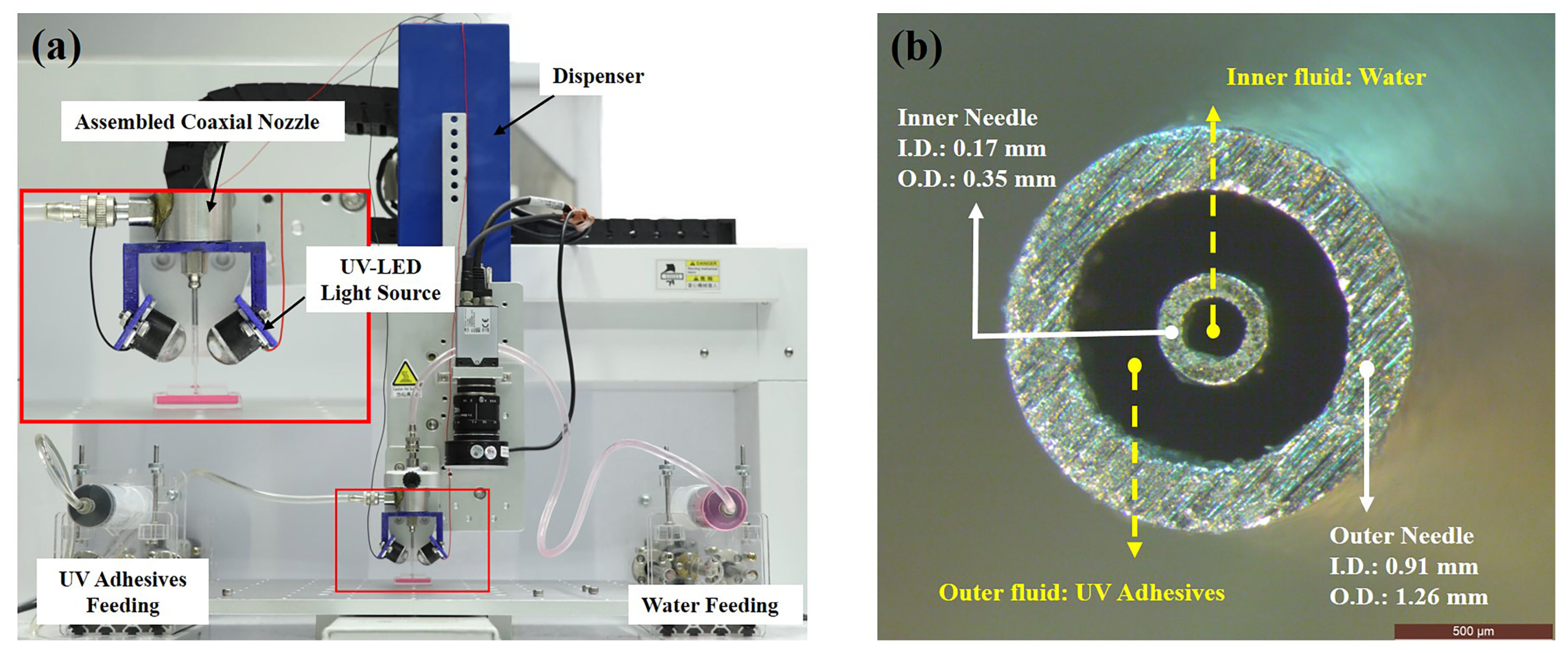
Figure 1. Experimental setup: (a) the total UV-assisted coaxial 3D printing system consisted of a commercial dispenser, an assembled coaxial nozzle, a UV-LED light source, and two syringe drivers for fluids feeding; and (b) bottom view of the assembled coaxial nozzle without the transparent jacket where the outer needle (ID 0.91 mm, OD 1.26 mm) for UV adhesives and the inner needle (ID 0.17 mm, OD 0.35 mm) for water.
Applsci 10 03384 g001
Figure 2. The converged UV-LED light source design and its simulation results: (a) the converged UV-LED light source attached to the coaxial nozzle; (b) dimension clarification of the converged UV-LED; (c) the total UV radiation area in an ellipse shape with a length and width of around 13 and 10 mm, respectively; and (d) the UV radiation for the pre-curing, which the intensity was estimated to an average of 1.45 W/ cm 2 with the area of 1 × 6 mm 2 .
Applsci 10 03384 g002
Figure 3. Fabrication process of a typical PDMS–Glass microfluidic device with printed connectors.
Applsci 10 03384 g003
Figure 4. UV rheological characterization results: (a) viscosity as a function of UV exposure time (365 nm, 1 W/ cm 2 ); and (b) moduli as a function of UV exposure time (365 nm, 1 W/ cm 2 ). The gelation point is defined as the cross over point of the storage modulus G’ and the loss modulus G”.
Applsci 10 03384 g004
Figure 5. The relationship between gelation time and UV intensity.
Applsci 10 03384 g005
Figure 6. Co-flow behavior regimes and region: (a) different co-flow behavior regimes including dripping, outer flow, undulant jetting, and threading jetting; and (b) concluded co-flow behavior region.
Applsci 10 03384 g006
Figure 7. (a) Schematic of material conversion mechanism in printing. Typical printing results in pre-cure time investigation: (b) hollow structure with thinning and swelling when pre-cure time at 4 s; and (c) uniform-shaped hollow structure with a well constrained inner channel when pre-cure time at 6 s.
Applsci 10 03384 g007
Figure 8. Dimension clarification and magnified view of successfully printed hollow connector.
Applsci 10 03384 g008
Figure 9. Demonstration of printed connectors for microfluidic interconnections: overview (a); top view (b); and side view (c) of the typical PDMS–Glass microfluidic device with printed hollow connectors.
Applsci 10 03384 g009
Table 1. Comparison of microfluidic interface solutions.
SolutionsMechanical
Property
Interconnect
Density
Clogging
Issue
Target
Material
Fabrication
Efficiency
Cost
DRIE interlock
structures [7,8]
PoorHighNoSiliconLowHigh
Tubings or needles
through punched
holes [11,12]
FairHighNoPDMSHighLow
Ultrasonic welding [16,17]GoodModerateYesThermopalsticHighModerate
Adhesive gluing [18,19]GoodHighYesAllHighLow
Fixing accessories [20,21,22,23,24,25,26]GoodModerate
/Low
NoAllModerate
/Low
Moderate
Monolithic 3D printed
connectors [30,31]
FairModerateNoPhotosensitive resin
/thermoplastic
HighModerate
This workGoodModerateNoAllHighModerate
Table 2. Input parameters in Tracepro ray-tracing.
MaterialRefractive Index at 365 nmAbsorption Coefficient at 365 nm ( mm 1 )
Glass1.540.001
Aluminum0.40 1.52 × 10 5
Silicone1.540.12
Table 3. Gelation time under different UV intensity (n = 1).
UV Intensity (W/ cm 2 )0.51.01.52.02.53.05.0
Gelation Time (s)10.06.96.47.67.26.33.8
Table 4. Success rate of uniform-shaped hollow connectors printing (n = 10).
Pre-Cure Time (s)23455.566.57.5
Success rate0%0%0%20%50%100%100%100%