Abstract
This paper targets on the design and analysis of specific types of transfer functions obtained by the summing operation of integer-order and fractional-order two-port responses. Various operations provided by fractional-order, two-terminal devices have been studied recently. However, this topic needs to be further studied, and the topologies need to be analyzed in order to extend the state of the art. The studied topology utilizes the passive solution of a constant-phase element (with order equal to 0.5) implemented by parallel resistor–capacitor circuit (RC) sections operating as a fractional-order two-port. The integer-order part is implemented by operational amplifier-based lossless integrators and differentiators in branches with electronically adjustable gain, useful for time constant tuning. Four possible cases of the fractional-order and integer-order two-port interconnections are analyzed analytically, by PSpice simulations and also experimentally in the frequency range between 10 Hz and 1 MHz. Standard discrete active components are used in this design for laboratory verification. Practical recommendations for construction and also particular solutions overcoming possible issues with instability and DC offsets are also given. Experimental and simulated results are in good agreement with theory.
1. Introduction
Circuit designs using fractional-order devices require a special type of analysis and evaluation because the resulting behavior of these systems is quite different and more complex than in cases of standard integer-order designs. Frequency responses influenced by the fractional-order behavior of used components are studied more frequently in recent years [1]. Many works in this field focus on novel solutions of integral and derivative two-ports (for example [2,3,4,5,6,7,8,9]), proportional integral and derivative controllers (for example [10,11,12,13,14,15,16,17,18] and so-called bilinear two ports [8,9,19,20,21] serving for various purposes. Two ports, known as integrators and differentiators, have started to be interesting for designers of fractional-order systems, and especially for proportional, integral and derivative controllers (PIDs). However, these systems are analyzed as complete solutions, and their transfer functions are considered in overall form (sum of all three responses).
The overview of typical examples dealing with the design of fractional-order integrators and differentiators (from the above discussed groups) is given in Table 1.

Table 1.
Comparison of standalone fractional-order integrator/differentiator solutions and solutions included in designs of controllers and other relevant design approaches.
D. Mondal et al. [2] brought a solution of the lossless integrator using a fractional-order passive element (FOE), known also as constant phase element (CPE) as a part of feedback loop of operational amplifier (OA) followed by inverter. However, adjustability and other features (two different slopes in magnitude frequency responses, various starting and final phase shifts in observed bandwidth, etc.) are not studied. D. Goyal et al. [3] presents integrators/differentiators implemented by complex active CMOS circuitry with the benefit of simple electronic reconfiguration. A similar approach was used by G. Tsirimokou et al. [4] where resulting integrators/differentiators are used for the design of a special type of filter performing also the sum/subtraction of current outputs. The synthesis of an active emulator of FOE based on operational transconductance amplifiers and its implementation in an OA-based lossless integrator is shown by G. Tsirimokou et al. [5]. Special active building blocks used in works [3,4,5,8] utilize approximation of the fractional-order behavior by higher-integer-order filtering responses allowing the electronic configuration of transfer coefficients (numerator/denominator). Similarly, G. Tsirimokou et al. [6], there is a discrete solution of this topology using passive parameters for appropriate configuration of the transfer. Topology presented by S. Kapoulea [7] represents one from the simplest examples of device using passive form of FOE-based on serial/parallel interconnections of RC segments. R. Sotner et al. [9] introduces method for the electronic rescalability of the operational bandwidth of the fractional-order integrator, by single DC voltage controlling several capacitance multipliers. Similarly to G. Tsirimokou et al. [6], this topology uses passive parameters for the setting of the response approximating required fractional-order behavior. Note that except R. Sotner et al. [9], there was no attempt to obtain single a parameter electronic adjustability of time constant in the area of fractional-order two-ports (integrators/differentiators).
Many interesting solutions of two-port interconnections have been presented as parts of various fractional-order controllers [10,11,12,13,14,15,16,17,18]. Many of them are using standard topologies based on OA [10,11] because of their simplicity. Some approaches target on extensive and complex design, based on field programmable analog arrays (FPAAs) [12] and field programmable gate arrays (FPGAs) [16], [17] because of their programmability. Moreover, FPGA represents a digital-only solution of the design. It allows the integration of highly complex topologies [12,16,17], but certain latency and delay of processing may occur in some cases. However, a significant drawback of these concepts is the necessity of software development and also quite high costs in comparison to a simple analog solution. Special analog active devices (with controllable internal parameters) used in the synthesis of controllers bring certain advantages in the simplification of the design and possibility of electronic adjustability/reconfigurability at the same time [13,14,15].
So-called bilinear synthesis brought significant contributions to the adjustability of the features of fractional-order devices [8,18,19,20,21]. Electronic tuning of zero and pole frequencies allows one to form an almost arbitrary frequency response with very simple and immediate reconfiguration [8,19,20,21].
Analysis of known solutions leads to the following conclusions:
- (a)
- Many proposed circuitries (except FPAA, FPGA-based) have quite complex topology, with many active and/or passive elements [9,12,16,17,18,19], especially circuits with fractional-order behavior and approximations by higher-order filters [3,5,6,13] or chain of bilinear segments [8,9,14,15,18,19,20,21],
- (b)
- some concepts require software programming [12,16,17],
- (c)
- tested operational bandwidth is quite narrow in many cases [3,4,5,7,8,11,12,13,18],
- (d)
- summing of fractional-order as well as integer-order two ports was not analyzed deeply in the past,
- (e)
- single-parameter electronic adjustment of the time constant of the resulting response of two-port summing was not studied in the past, except R. Sotner et al. [9], but the overall circuit topology is based upon a chain of bilinear sections, and therefore, it is not one of the simplest solutions
Despite the presence of various solutions of the above-mentioned two-ports, the effects of their mutual interconnections are studied rarely [4,8]. The most known cases of integral and derivative responses used simultaneously can be found in the field of controllers [7,10,11,12,13,14,15,16,18]. However, a detailed study of resulting responses is often omitted.
The first work (Tsirimokou et al. [22]), where various simple interconnections of fractional-order devices has been studied, targets on combinations of two-ports. This work gives the evaluation of the resulting impedance functions of serial/parallel interconnections of fractional-order capacitors (RC approximants), where each two-terminal is actually represented by an active solution allowing simple electronic configurability and also floating implementation. Experimental tests were performed for very low frequencies (<1 kHz). Kartci et al. [23] introduced work dealing with more complex interconnections of real solid-state, fractional-order two-terminals. However, despite further attempts in the synthesis of passive [24,25] or active [26] two-terminals, there are no attempts studying both simple and complex interconnections of fractional-order and integer-order two-ports. Moreover, the area of theoretical knowledge of fractional-order systems significantly extends into practical industrial applications [27].
To the best of the authors’ knowledge, a similar study targeting on interconnections of fractional and integer order two-ports has not been presented in literature. However, there are many particular cases that should be studied. This work focuses deeply on the behavior of the sum of two branches, including fractional-order, two-port (differentiator or integrator) and integer-order two port (differentiator or integrator). Features of resulting responses are studied theoretically, by PSpice simulation, and also experimentally. The practical notes for the construction of these interconnections of two-ports are also given. The initial work in this field was presented as conference paper [28]. However, very limited example of test cases was presented. In the case of this paper, the setting is totally different and also the types of active devices are not the same.
This work targets on:
- (a)
- the derivation of analytical expressions for mixed transfers, including sum of integer and fractional-order two-ports,
- (b)
- a single parameter electronic adjustment of the respective time constants,
- (c)
- the practical verification and also precautions of real implementation,
- (d)
- an extension of the state of the art in the field of serial/parallel interconnections of fractional-order two-terminal passive elements [22,23] to the two-port area.
The rest of this paper has the following organization: Section 2 describes the general block concept of the tested two-port interconnections. Section 3 shows features of the CPE element (RC approximant) used in analyzed cases. Section 4 presents four possible combinations of integrator and differentiator (fractional- and integer-order transfer branch) when summing their output responses, and it shows their analytical analysis. Practical issues in tested topologies, as well as possible solutions/compensations of these effects are discussed in Section 5. Section 6 introduces experimental results, and Section 7 concludes this work.
2. General Concept of Two-Port Interconnection
This work introduces the way of analyzing behavior of the resulting response of a sum of lossless integrator and differentiator where each of them has integer as well as fractional-order character (Figure 1). We will also observe the impact of the gain variation (designated as A1 and A2 in Figure 1) on the features of each path. We decided to study four particular cases: (a) integer-order integrator + fractional-order integrator, (b) integer-order differentiator + fractional-order differentiator, (c) integer-order integrator + fractional-order differentiator, (d) integer-order differentiator + fractional-order integrator.
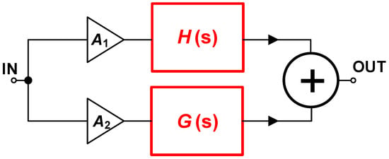
Figure 1.
General concept of all four analyzed systems (responses).
The transfer of the generalized system has form:
where partial transfers H(s) and G(s) are as follows:
where the particular index of H(s) and G(s) indicates the character of the accumulating device used in a particular two-port, and τ1,2 are initial values of the time constants.
Commercially-available, active devices can be used for purposes of practical verification of the concept from Figure 1 [29]. Variable gain amplifiers (VGAs) providing control of A1 and A2 gains will be based on VCA810 devices [30], the standard concept of the integrator and differentiator topology will utilize the LT1364 operational amplifier [31], and the sum operation is easily achievable by an AD8130 element [32]. In order to obtain fractional-order integrator or differentiator topology, a fractional-order element is required. The Constant Phase Element (CPE) is one of the possibilities described in the next section. The following subsections describe each of the four considered topologies, together with the most significant simulation and experimental results.
3. Passive Solution of Constant Phase Element
We selected CPE having order α = 0.5 with Cα = 56 μF/s1/2 for all experimentally studied cases (presented in Section 6). Its practical implementation by RC passive topology is shown in Figure 2, as well as its ideal and simulated magnitude and phase impedance characteristics. The phase accuracy of this CPE reaches ∆ϕα = ±2° in the theoretical operational bandwidth between 1 Hz and 3 MHz. The design was performed by the algorithm explained in several works in detail [14,33,34].
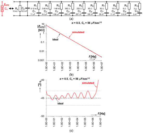
Figure 2.
Practical implementation of the Constant Phase Element (CPE) solution from resistor–capacitor circuit (RC) segments: (a) circuit topology; (b) magnitude of impedance; (c) phase of impedance.
4. Analytical Analysis of Two-Port Interconnections
We divided ideal analysis to four sections in accordance to discussion in Section 2. Each interconnection is represented by real circuit topology, including all used active devices and values of used passive elements, as well as compensating elements improving stability as will be explained later. Note that compensating passive elements, drawn in the figures by dashed lines, are excluded from analytical analysis because of simplicity. The following ideal analyses use τ1(integer) = 100 μs, τ2(fractional/CPE) = 5.6 ms and fixed A1 = A2 = 1.
4.1. Sum of Integer and Fractional-Order Integrator Responses
Practical circuitry implementing the fractional-order integrator and integer-order integrator derived from the general concept in Figure 1 is shown in Figure 3. Its transfer function is given by:
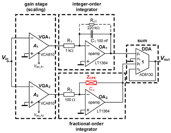
Figure 3.
Practical solution of circuitry providing summing responses of the fractional- and integer-order integrators.
Its representation in complex form is quite extensive:
Magnitude and phase part can be expressed as, respectively:
The Mathcad analysis of ideal transfer function (10) is shown in Figure 4 as three dimensional (3D) plots. Variation of order α between 0 and 1 indicates a clear point of break where the slope divides into two parts (integer-order low-frequency zone and fractional-order high-frequency zone), and the movement of position of this intentional zero from high frequencies to low frequencies, as well as increasing the character of the corner phase shift at the end of the operational band (from −90° up to 0°).
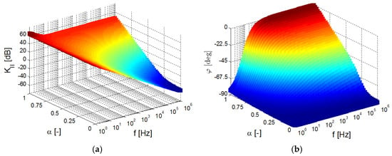
Figure 4.
The three dimensional (3D) plot of studied ideal transfer response (10) in dependence on the value of the α variable: (a) magnitude vs. order vs. frequency dependence, (b) phase vs. order vs. frequency dependence.
4.2. Sum of Integer and Fractional-Order Differentiator Responses
Figure 5 shows interconnection resulting from the summing operation of integer and fractional-order differentiator responses. The transfer function can be expressed as:
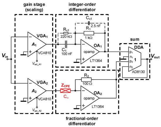
Figure 5.
Practical solution of the summing response of fractional- and integer order differentiator.
The rearrangement into complex form leads to:
and after separation to magnitude and phase response we obtain:
The Mathcad analysis of the transfer function (14) is shown in Figure 6. It shows that order variation (the same as in the previous case) causes a very similar point of break on the magnitude slope and occurrence of zero at low frequencies (especially for orders near to 1), and the cut of the plane projection of the phase response confirms that this starting phase value (low frequencies) clearly depends upon the value of the α order.
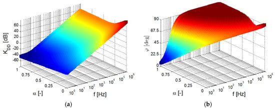
Figure 6.
3D plot of the studied ideal transfer response (14) in dependence on the value of the α variable: (a) magnitude vs order vs frequency dependence, (b) phase vs order vs frequency dependence.
4.3. Sum of Integer-Order Integrator and Fractional-Order Differentiator Responses
This topology has behavior indicating a significant global minimum of the ideal transfer magnitude because the decreasing and increasing magnitude in frequency response is given by the interconnection of the integrator and differentiator (Figure 7). The response has this form:
that can be easily modified to the complex expression:
and the resulting magnitude and phase responses of the two-port are:
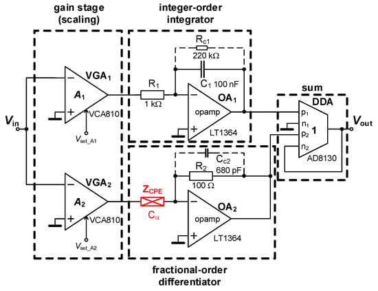
Figure 7.
Practical solution of the summing response of fractional-order differentiator and integer order integrator.
The ideal analysis of (18) shown in Figure 8 indicates two-sides of the magnitude response with different slopes and significant local minimum. The phase plot confirms the impact of the order on the phase value in high-frequency corner (between 0° and 90°).
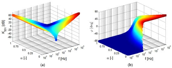
Figure 8.
The 3D plot of studied ideal transfer response (18) in dependence on value of the α variable: (a) magnitude vs order vs frequency dependence, (b) phase vs order vs frequency dependence.
4.4. Sum of Fractional-Order Integrator and Integer-Order Differentiator Responses
The last considered combination of integer-order and fractional-order response is shown in Figure 9. The resulting frequency response is quite similar to the previous case:
again, we can modify it to the complex form:
and we can express the corresponding magnitude and phase responses:
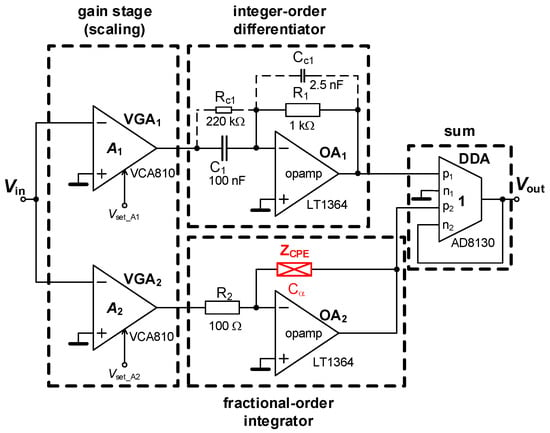
Figure 9.
Practical solution of the summing response of fractional-order integrator and integer-order differentiator.
The 3D plot in Figure 10 also reports the significant global minimum of transfer (as expected). However, the sides of both slopes are opposite with respect to the previous case. The cut in phase projection shows the initial phase value (low-frequency corner) dependence on the order (start between −90° and 0°).
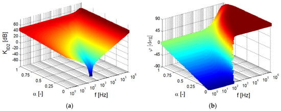
Figure 10.
The 3D plot of the studied ideal transfer response (22) in dependence on the value of α variable: (a) magnitude vs order vs frequency dependence, (b) phase vs order vs frequency dependence.
5. Solving Non-Ideal Issues during the Tests
Note that the bridging resistor Rc1, being part of each of the presented summing solutions, intentionally limits the direct current (DC) gain of OA1 to a finite value (≅200) in order to minimize the impacts of the saturation of the output because of nonzero DC offset caused by real asymmetry of the active elements. Moreover, effects of high-gain blocks, as well as remaining DC offsets, require manual compensations by DC voltage applied against real DC offset, as shown in Figure 11. These compensations are required in both paths of the studied topology. In our case, the input DC offsets reach values of tens of mV, approximately. However, it was sufficiently high to cause saturation (Vout = VDD or VSS) of the OA output. Therefore, the compensation was provided really carefully. Note that the output DC shift above ±50 mV causes a significant effect on the frequency response accuracy.
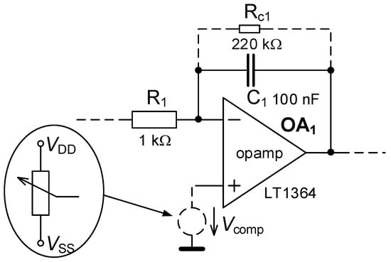
Figure 11.
Principle of intentional DC gain limitation and compensation of DC offset and asymmetry of inputs in the case of integer-order branch given as an example.
Moreover, also damping of unintentional oscillations should be done by a parallel connection of the capacitor to the feedback resistor in the OA network, as shown in Figure 12. Note that gain caused by the derivative character of the branch increases with frequency (more than 40 dB above 100 kHz). The compensation of instability by additional CC1 and CC2 elements was prepared to suppress the resonant peak approximately between 200 and 300 kHz, as shown in Figure 5, Figure 7 and Figure 9. Despite quite high values of CC-s, the value of this intentional frequency zero is quite high because of parallel resistors having low value (100 Ω and 1 kΩ). The approximate value of compensating zero frequency can be calculated as fzC = 1/(2·π·R1CC1). For values included in Figure 12 it is 63 kHz. It indicates that influences causing possible instability and oscillations above 100 kHz are sufficiently suppressed.
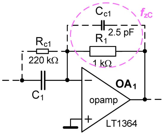
Figure 12.
An example of frequency compensation of instability in integer-order branch given as an example.
6. Experimental Analysis
Two-ports discussed above were analyzed in PSpice software and also experimentally with real devices. We used oscilloscope Keysight DSOX3022T with the Frequency Response Analysis (FRA) option [35] for time domain as well the as frequency domain testing. The input signal level used in tests was approximately 30 mVP-P because of the significant change of gain, and it was constant in the whole observed band (20 Hz–1 MHz). The simultaneous time-domain and frequency-domain measurements, enabled by this oscilloscope during the point-to-point FRA analysis, were necessary due to clear visibility of the correct setting of DC offset error compensation.
We can calculate initial time constants of the OA-based integrator/differentiator directly from values shown in Figure 3, Figure 5, Figure 7 and Figure 9: τ1(integer) = 100 s (R1 × C1 = 1 kΩ × 100 nF), τ2(fractional/CPE) = 5.6 ms (R2 × Cα = 100 Ω × 56 μF/s1/2). The driving voltages Vset_A1 and Vset_A2 for the time constant adjustment by gains A1 and A2 are considered between 0.85 and 1.35 V (A1,2 between 0.5 and 5 because A1,2 = 10(2∙(Vset_A1,2 − 1)) [30]) in order to observe a one-decade change of gain. However, increased gain requires compensation of instability as well as DC offset (VGA output offset depends on actual gain), as discussed above. Particular values of gains A1,2 are noted directly in presented graphs. Note that our design targets are on the low-frequency band of operation (application field between 100 Hz and 100 kHz) because of expected limits (DC offset impacts for high gain scale, instability) of active devices as well as simpler design for our exemplary purposes.
6.1. Analysis of Integer-and Fractional-Order Integrators and Differentiators
The frequency responses of key parts of the system (integrators/differentiators using integer- or fractional-order capacitor) are studied before analysis of the response of the whole system (Figure 1). Results are shown in Figure 13 for the integral branch and in Figure 14 for the derivative branch. Above discussed parameters of time constants are valid also for this case. The operational bandwidth of the integrators (considering phase changes) is limited into the range approximately between 50 Hz and 200 kHz. The operational band of differentiators is significantly lower (only 50 Hz–10 kHz) due to high-frequency limitations and parasitic poles (and their intentional compensation) in case of a real transfer function.
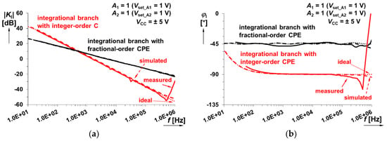
Figure 13.
Frequency response of integer-order and fractional-order integrator: (a) magnitude responses; (b) phase responses.
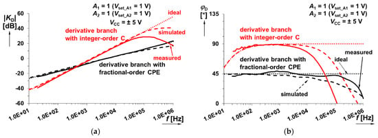
Figure 14.
Frequency response of integer-order and fractional-order differentiator: (a) magnitude responses; (b) phase responses.
6.2. Analysis of Sum of Integer and Fractional-Order Integrator Responses
The experimental setup for this system shown in Figure 3 (both branches are integrators) is analyzed in this subsection. We separated results for the variation of individual scaling gains A1 and A2 (0.5→5) to Figure 15 and Figure 16. While one gain was changed, the other one was set to a constant value of 1.
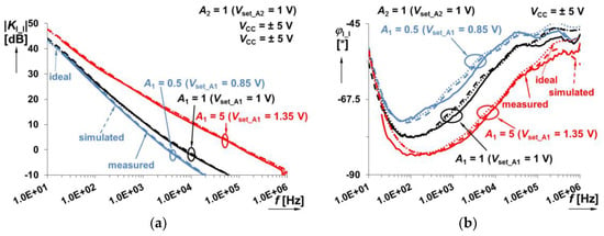
Figure 15.
Frequency response of the system shown in Figure 3 (sum of integer- and fractional-order integrator responses) when A1 (integer-order branch) is varying between 0.5 and 5: (a) magnitude responses; (b) phase responses.
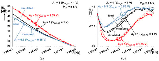
Figure 16.
Frequency response of system in Figure 3 (sum of integer- and fractional-order integrator responses) when A2 (fractional-order branch) is varying between 0.5 and 5: (a) magnitude responses; (b) phase responses.
The measured time domain responses were studied in more detail at frequency in the middle of the considered band (10 kHz). Output responses on square-wave as well as triangular input voltage are shown in Figure 17 for A1 = A2 = 1.
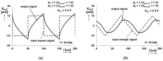
Figure 17.
Time domain response of system in Figure 3 (sum of integer- and fractional-order integrator responses) when sourced by: (a) square wave input signal; (b) triangular wave input signal.
The change of gains A1, A2 allows one to set time constants of both paths independently (theoretically: τ1 ∈ (200 μs, 20 μs) and τ2 ∈ (11 ms, 1.1 ms) for A1,2 ∈ (0.5, 5.0)) and therefore also the frequency position of the point of break can be electronically controlled. It can be useful for controllers requiring immediate change on their response.
6.3. Analysis of Sum of Integer and Fractional-Order Differentiator Responses
This system shown in Figure 5 consists of differentiators in both branches. The achieved behavior is indicated in Figure 18 and Figure 19 (again for the same values of A1,2 gains). Example of time domain analysis of the output response is shown in Figure 20.
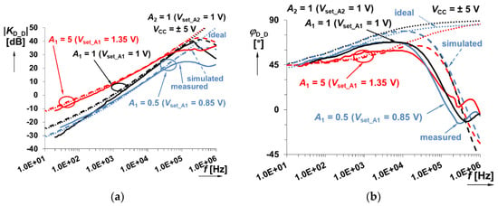
Figure 18.
Frequency response of the system shown in Figure 5 (sum of integer- and fractional-order differentiator responses) when A1 (integer-order branch) is varying between 0.5 and 5: (a) magnitude responses; (b) phase responses.
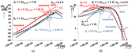
Figure 19.
Frequency response of this system shown in Figure 5 (sum of integer- and fractional-order differentiator responses) when A2 (fractional-order branch) is varying between 0.5 and 5: (a) magnitude responses; (b) phase responses.
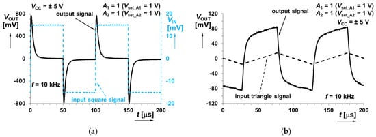
Figure 20.
Time domain response of the system in Figure 5 (sum of integer- and fractional-order differentiator responses) when sourced by: (a) square wave input signal; (b) triangular wave input signal.
6.4. Analysis of Sum of Integer-Order Integrator and Fractional-Order Differentiator Responses
This specific case shown in Figure 7 implements the sum of integer-order integrator and fractional-order differentiator. Figure 21 and Figure 22 indicate expected minimum of transfer (magnitude) given by intentional zero frequencies. Figure 23, Figure 24 and Figure 25 show particular time-domain wave forms at frequencies in area with dominance of integration (800 Hz), differentiation (100 kHz), as well as a frequency of 7 kHz being close to the gain minimum (selected example for A1 = 5, A2 = 1).
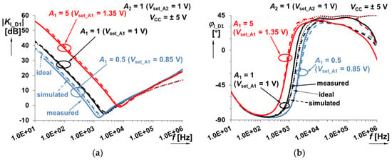
Figure 21.
Frequency response of the system shown in Figure 7 (sum of integer-order integrator and fractional-order differentiator responses) when A1 (integer-order branch) is varying between 0.5 and 5: (a) magnitude responses; (b) phase responses.
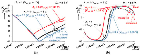
Figure 22.
Frequency response of the system shown in Figure 7 (sum of integer-order integrator and fractional-order differentiator responses) when A2 (fractional-order branch) is varying between 0.5 and 5: (a) magnitude responses; (b) phase responses.
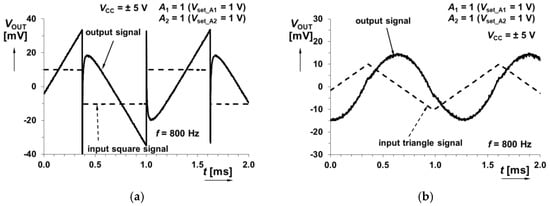
Figure 23.
Time domain response of the system shown in Figure 7 (sum of integer-order integrator and fractional-order differentiator responses) at 800 Hz when sourced by: (a) square wave input signal; (b) triangular wave input signal.
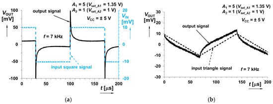
Figure 24.
Time domain response of the system shown in Figure 7 (sum of integer-order integrator and fractional-order differentiator responses) at 7 kHz when sourced by: (a) square wave input signal; (b) triangular wave input signal.
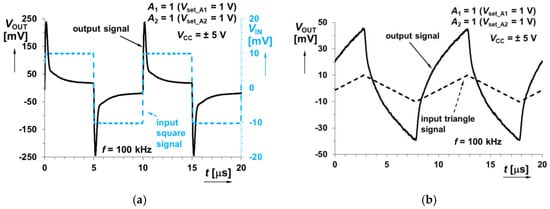
Figure 25.
Time domain response of the system shown in Figure 7 (sum of integer-order integrator and fractional-order differentiator responses) at 100 kHz when sourced by: (a) square wave input signal; (b) triangular wave input signal.
6.5. Analysis of Sum of Fractional-Order Integrator and Integer-Order Differentiator Responses
The last combination of interconnection shown in Figure 9 (sum of fractional-order integrator and integer-order differentiator) was also analyzed, and frequency responses are provided in Figure 26 and Figure 27. Time domain analysis focuses on results obtained at three different frequencies similarly to the previous case (at 600 Hz in the range influenced by fractional-order behavior, at 2.15 kHz at the minimal gain visible for the selected gain setting A1 = A2 = 1, and for 50 kHz in the derivative area). Results are shown in Figure 28, Figure 29 and Figure 30.
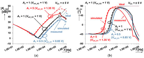
Figure 26.
Frequency response of the system shown in Figure 9 (sum of fractional-order integrator and integer-order differentiator responses) when A1 (integer-order branch) is varying between 0.5 and 5: (a) magnitude responses; (b) phase responses.
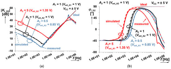
Figure 27.
Frequency response of the system shown in Figure 9 (sum of fractional-order integrator and integer-order differentiator responses) when A2 (fractional-order branch) is varying between 0.5 and 5: (a) magnitude responses; (b) phase responses.
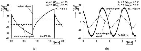
Figure 28.
Time domain response of the system in Figure 9 (sum of fractional-order integrator and integer-order differentiator responses) at 600 Hz on: (a) square wave input signal; (b) triangular wave input signal.
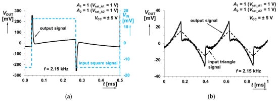
Figure 29.
Time domain response of the system in Figure 9 (sum of fractional-order integrator and integer-order differentiator responses) at 2.15 kHz on: (a) square wave input signal; (b) triangular wave input signal.
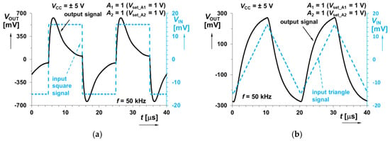
Figure 30.
Time domain response of the system in Figure 9 (sum of fractional-order integrator and integer-order differentiator responses) at 50 kHz on: (a) square wave input signal; (b) triangular wave input signal.
Results presented in this section (Section 6) indicate quite good correspondence of theoretical expectations and experiments. However, high-frequency limitations of active devices as well as other small-signal parasitics influence the high-frequency band significantly. The substantial resonant peak occurs at a frequency around 200–300 kHz. Generally, the frequency limits also depend upon the accuracy of CPE, and therefore, also on used approximation. However, in our case, active devices and real circuitry has significantly higher impact. The resulting operational bandwidth of discussed systems can be determined between 50 Hz and 100 kHz for both branches, using integrators (fractional and integer-order), between 50 Hz and 10 kHz for both branches, including differentiators, between 50 Hz and 10 kHz for the sum of integer-order integrator and fractional-order differentiator, and finally between 50 Hz and 10 kHz for the sum of fractional-order integrator and integer-order differentiator. The signal dynamics overcomes 40 dB in all presented tests. Therefore, large gain variation occurs, and signals reach very low (tens of mV), as well as very high values (hundreds of mV). It should be considered carefully in the design.
We evaluated selected results of magnitude and phase frequency response (Figure 22) for interconnection in Figure 7 (Section 4.3). The evaluation of simulated and measured frequency responses in the selected case (integer-order integrator and fractional-order differentiator) yields a maximal difference of magnitude of 7 dB in the tested band (10 Hz–1 MHz) and 1.1 dB in the expected (precise) operational range (50 Hz–10 kHz). The deviation 7 dB means the largest magnitude error is about 40% (at high frequencies above 500 kHz) between measured and simulated traces. However, the error is below 12% in the operational band (up to 10 kHz). Note that the relative error (%) seems to be large (tens of %) for small values of gain in units of dB, but the absolute error is acceptable. The phase difference reaches 11° maximally (10 Hz–1 MHz) and 4° (around 10% error) in the suggested operational band (50 Hz–10 kHz). The very similar behavior of all responses indicates that very similar differences are valid also for other cases (magnitude differences between 1–2 dB and phase differences up to 10–15° in the range between 50 Hz and 10 kHz, and higher phase differences especially for integer-order differentiator, as shown in Figure 14).
The results indicate that the specific position of the fractional-order device, as well as the particular combination of two-ports influences slope (point of break in the case of two integrators or two differentiators in resulting topology), or creates a global minimum (combination of integrator and differentiator in resulting topology) and an initial or final phase value in the operational band. Electronic adjustment of transfer responses (gains A1, A2) in both paths may be useful for special control applications where the position of global minimum (or point of break) should be impacted immediately in order to optimize effectiveness of regulation during the operation.
Table 2 summarizes the results of maximally achievable magnitude slopes and phase shifts for a theoretical variation of the α parameter and typical experimental results for our case α = 0.5 tested in detail. Presented solutions divide the frequency characteristic to two sub-bands (low-frequency and high-frequency—below and above the point of break or global minimum). The fractional-order two-port has a capability to set the initial or final phase shift as well as the slope of magnitude in a specified sub-band arbitrarily in dependence on the α value. The best accuracy with theory was obtained for solutions in Figure 7 and Figure 9. Solutions in Figure 3 and Figure 5 reflect the imperfections and effects of real active devices at high frequencies and the initial behavior of RC approximant at low frequencies, all due to very high processed dynamics in the observed bandwidth.

Table 2.
Summarization of theoretical features and experimentally obtained results for studied case (α = 0.5).
7. Conclusions
Four experimentally tested cases of interconnections summing the fractional- and integer-order differentiators and integrators brought interesting results. General operationability of the concepts is limited by the real features of active devices used. The most significant impact has DC accuracy and variable DC offset dependent on the actual setting of gain in the frame of the VGA as well as high-frequency parasitic poles occurring for high gains (differentiator operation). We can state that the proposed concept is approximately operable from 50 Hz up to 10 kHz in all cases.
The gain changes reached more than 45 dB in the observed frequency band (amplification/attenuation of more than 170 times). Therefore, very careful selection of testing input voltage levels is required. The input excitation should be selected in dependence on a particular type of interconnection, but still in range of low tens of mV (30 mVP-P used in tests). However, in specific cases, the input level can reach higher values (hundreds of mV) when operation with low dynamics in limited bandwidths of specific transfer responses (and configurations) is supposed. The expected slopes of experimentally obtained magnitude responses have differences between 1–4 dB/dec from an ideal case in the observed operational bandwidth (50 Hz–10 kHz). The phase responses achieves good results for lower corner phase shifts (45°), where differences from this ideal case are about 3–4° maximally. However, larger phase values at a high-frequency corner for integer-order differentiator are significantly influenced (differences of 10–12° from ideal value) by the frequency limitations of real circuitry (parasitic poles and zeros). The expected maximal differences of measured and simulated traces of frequency responses (in suggested operational bandwidth: 50 Hz–10 kHz) reaches 1–2 dB in magnitude and up to 10–15° (especially at high frequencies due to parasitic behavior of real circuitry). Adjustability of gains in both paths allows influence on the shape of the resulting response in dependence on the specific character of each path (integrator/differentiator) because of their impact on a local minimum or breakpoint. The initial and final phase response can be influenced by the selected α order. Experimental verifications confirmed the expected behavior of the systems quite precisely and obtained results have good correspondence with both simulations and theory. Presented analyses are useful for further applications of studied systems, for example in the design of proportional, integral and derivative controllers or special cases of signal processing requiring these types of transfers (decreasing and increasing gains with different slopes).
Author Contributions
Conceptualization, R.S. and O.D.; Methodology, R.S., O.D. and J.P.; Validation, R.S., O.D., and J.J.; Formal Analysis, J.J., N.H., J.P., and D.A.; Investigation, R.S., O.D., J.J., N.H., and J.P.; Data Curation, J.J., N.H., and D.A.; Writing—Original Draft Preparation, R.S., O.D., J.J., and N.H.; Writing—Review and Editing, R.S., O.D., J.J., and N.H. All authors have read and agreed to the published version of the manuscript.
Funding
This article is based upon work from COST Action CA15225, a network supported by COST (European Cooperation in Science and Technology). Research described in this paper was financed by the National Sustainability Program under grant LO1401 and by the Ministry of Education, Youth and Sports under grant LTC18022 of Inter-Cost program. For the research, infrastructure of the SIX Center was used.
Acknowledgments
Authors wish to thank the reviewers for their useful comments.
Conflicts of Interest
The authors declare no conflict of interest.
References
- Elwakil, A.S. Fractional-order circuits and systems: An emerging interdisciplinary research area. IEEE Circuits Syst. Mag. 2010, 10, 40–50. [Google Scholar] [CrossRef]
- Mondal, D.; Biswas, K. Performance study of fractional order integrator using single-component fractional order element. IET Circuits Devices Syst. 2011, 5, 334–342. [Google Scholar] [CrossRef]
- Goyal, D.; Varshney, P. Analog Realization of Electronically Tunable Fractional-Order Differ-Integrators. Arab. J. Sci. Eng. 2019, 44, 1933–1948. [Google Scholar] [CrossRef]
- Tsirimokou, G.; Psychalinos, C. Ultra-low voltage fractional-order circuits using current mirrors. Int. J. Circuit Theory Appl. 2016, 44, 109–126. [Google Scholar] [CrossRef]
- Tsirimokou, G.; Psychalinos, C.; Elwakil, A.S.; Salama, K.N. Experimental verification of on-chip CMOS fractional-order capacitor emulators. Electron. Lett. 2016, 52, 1298–1300. [Google Scholar] [CrossRef]
- Tsirimokou, G.; Kartci, A.; Koton, K.; Herencsar, N.; Psychalinos, C. Comparative Study of Fractional-Order Differentiators and Integrators. In Proceedings of the 40th International Conference on Telecommunications and Signal Processing (TSP), Barcelona, Spain, 5–7 July 2017; pp. 714–717. [Google Scholar]
- Kapoulea, S.; Psychalinos, C.; Elwakil, A.S. Single active element implementation of fractional-order differentiators and integrators. AEU Int. J. Electron. Commun. 2018, 97, 6–15. [Google Scholar] [CrossRef]
- Bertsias, R.; Psychalinos, C.; Elwakil, A.S.; Safari, L.; Minaei, S. Design and application examples of CMOS fractional-order differentiators and integrators. Microelectron. J. 2019, 83, 155–167. [Google Scholar] [CrossRef]
- Sotner, R.; Jerabek, J.; Langhammer, L.; Polak, L.; Jaikla, W.; Prommee, P. Operational Frequency Bandwidth Rescalable Implementations of Constant Phase Devices. In Proceedings of the 29th International Conference Radioelektronika, Pardubice, Czech Republic, 16–18 April 2019; pp. 1–6. [Google Scholar]
- Podlubny, I.; Vinagre, B.; O’leary, P.; Dorcak, L. Analogue realizations of fractional-order controllers. Nonlinear Dyn. 2002, 29, 281–296. [Google Scholar] [CrossRef]
- Charef, A. Analogue realisation of fractional-order integrator, differentiator and fractional PI/spl lambda/D/spl mu/ controller. IEE Proc. Control. Theory Appl. 2006, 153, 714–720. [Google Scholar] [CrossRef]
- Muniz-Montero, C.; Garcia-Jimenez, L.V.; Sanchez-Gaspariano, L.A.; Sanchez-Lopez, C.; Gonzalez-Diaz, V.R.; Tlelo-Cuautle, E. New alternatives for analog implementation of fractional-order integrators, differentiators and PID controllers based on integer order integrators. Nonlinear Dyn. 2017, 90, 241–256. [Google Scholar] [CrossRef]
- Dimeas, I.; Petras, I.; Psychalinos, C. New analog implementation technique for fractional-order controlled: A dc motor control. AEU Int. J. Electron. Commun. 2017, 78, 192–200. [Google Scholar] [CrossRef]
- Domansky, O.; Sotner, R.; Langhammer, L.; Jerabek, J.; Psychalinos, C.; Tsirimokou, G. Practical Design of RC Approximants of Constant Phase Elements and Their Implementation in Fractional-Order PID Regulators Using CMOS Voltage Differencing Current Conveyors. Circuits Syst. Signal Process. 2019, 38, 1520–1546. [Google Scholar] [CrossRef]
- Sotner, R.; Jerabek, J.; Kartci, A.; Domansky, O.; Herencsar, N.; Kledrowetz, V.; Alagoz, B.; Yeroglu, C. Electronically reconfigurable two-path fractional-order PI/D controller employing constant phase blocks based on bilinear segments using CMOS modified current differencing unit. Microelectron. J. 2019, 86, 114–129. [Google Scholar] [CrossRef]
- Tolba, M.F.; AboAlNaga, B.M.; Said, L.A.; Madian, A.H.; Radwan, A.G. Fractional order integrator/differentiator: FPGA implementation and FOPID controller application. AEU Int. J. Electron. Commun. 2019, 98, 220–229. [Google Scholar] [CrossRef]
- Tolba, M.F.; Said, L.A.; Madian, A.H.; Radwan, A.G. FPGA Implementation of the Fractional Order Integrator/Differentiator: Two Approaches and Applications. IEEE Trans. Circuits Syst. I Regul. Pap. 2019, 66, 1484–1495. [Google Scholar] [CrossRef]
- Herencsar, N.; Kartci, A.; Koton, J.; Sotner, R.; Alagoz, B.B.; Yeroglu, C. Analogue Implementation of a Fractional-PIλ Controller for DC Motor Speed Control. In Proceedings of the 28th IEEE International Symposium on Industrial Electronics (ISIE), Vancouver, BC, Canada, 12–14 June 2019; pp. 467–472. [Google Scholar]
- Sotner, R.; Jerabek, J.; Herencsar, N.; Petrzela, J.; Dostal, T.; Vrba, K. First-order adjustable transfer sections for synthesis suitable for special purposes in constant phase block approximation. AEU Int. J. Electron. Commun. 2015, 69, 1334–1345. [Google Scholar] [CrossRef]
- Sotner, R.; Petrzela, J.; Domansky, O.; Dostal, T. Current feedback operational amplifier based two-port frequency equalizer. In Proceedings of the European Conference on Circuit Theory and Design (ECCTD), Catania, Italy, 4–6 September 2017; pp. 1–4. [Google Scholar]
- Sotner, R.; Polak, L.; Jerabek, J.; Petrzela, J. Simple two operational transconductance amplifiers-based electronically controllable bilinear two port for fractional-order synthesis. Electron. Lett. 2018, 54, 1164–1165. [Google Scholar] [CrossRef]
- Tsirimokou, G.; Psychalinos, C.; Elwakil, A.S.; Salama, K.N. Experimental behavior evaluation of series and parallel connected constant phase elements. AEU Int. J. Electron. Commun. 2017, 74, 5–12. [Google Scholar] [CrossRef]
- Kartci, A.; Agambayev, A.; Herencsar, N.; Salama, K.N. Series-, Parallel-, and Inter-Connection of Solid-State Arbitrary Fractional-Order Capacitors: Theoretical Study and Experimental Verification. IEEE Access 2018, 6, 10933–10943. [Google Scholar] [CrossRef]
- Kartci, A.; Agambayev, A.; Farhat, M.; Herencsar, N.; Brancik, L.; Bagci, H.; Salama, K.N. Synthesis and Optimization of Fractional-Order Elements Using a Genetic Algorithm. IEEE Access 2019, 7, 80233–80246. [Google Scholar] [CrossRef]
- Semary, M.S.; Fouda, M.E.; Hassan, H.N.; Radwan, A.G. Realization of fractional-order capacitor based on passive symmetric network. J. Adv. Res. 2019, 18, 147–159. [Google Scholar] [CrossRef] [PubMed]
- Sotner, R.; Jerabek, J.; Petrzela, J.; Domansky, O.; Tsirimokou, G.; Psychalinos, C. Synthesis and design of constant phase elements based on the multiplication of electronically controllable bilinear immittances in practice. AEU Int. J. Electron. Commun. 2017, 78, 98–113. [Google Scholar] [CrossRef]
- Kadlcik, L.; Horsky, P. A CMOS Follower-Type Voltage Regulator with a Distributed-Element Fractional-Order Control. IEEE Trans. Circuits Syst. I Regul. Pap. 2018, 65, 2753–2763. [Google Scholar] [CrossRef]
- Sotner, R.; Petrzela, J.; Jerabek, J.; Herencsar, N.; Andriukaitis, D. Design of Fractional-Order Integrator Controlled by Single Voltage Gain. In Proceedings of the 42nd International Conference on Telecommunications and Signal Processing (TSP), Budapest, Hungary, 1–3 July 2019; pp. 360–364. [Google Scholar]
- Biolek, D.; Senani, R.; Biolkova, V.; Kolka, Z. Active elements for analog signal processing: Classification, review, and new proposal. Radioengineering 2008, 17, 15–32. [Google Scholar]
- Texas Instruments. VCA810 High Gain Adjust Range, Wideband and Variable Gain Amplifier. 2015. Available online: http://www.ti.com/lit/ds/symlink/vca810.pdf (accessed on 3 November 2019).
- Analog Devices. LT1364/LT1365 Dual and Quad 70 MHz, 1000 V/us Op Amps. 1994. Available online: https://www.analog.com/media/en/technical-documentation/data-sheets/13645fa.pdf (accessed on 3 November 2019).
- Analog Devices. AD8129/8130 Low Cost 270 MHz Differential Receiver Amplifiers. 2005. Available online: https://www.analog.com/media/en/technical-documentation/data-sheets/AD8129_8130.pdf (accessed on 3 November 2019).
- Valsa, J.; Dvorak, P.; Friedl, M. Network model of the CPE. Radioengineering 2011, 20, 616–626. [Google Scholar]
- Valsa, J.; Vlach, J. RC models of a constant phase element. Int. J. Circuit Theory Appl. 2013, 41, 59–67. [Google Scholar] [CrossRef]
- Keysight. Keysight InfiniiVision 3000T X-Series Oscilloscopes User’s Guide. 2017. Available online: https://www.keysight.com/main/techSupport.jspx?nid=-32541.1150349&pid=x202172&cc=CZ&lc=eng&pageMode=PL (accessed on 3 November 2019).
© 2019 by the authors. Licensee MDPI, Basel, Switzerland. This article is an open access article distributed under the terms and conditions of the Creative Commons Attribution (CC BY) license (http://creativecommons.org/licenses/by/4.0/).