1. Introduction
Resistive sensors are widely applied in various forms, such as temperature, pressure, humidity, and gas sensors [
1,
2,
3,
4,
5,
6,
7,
8,
9,
10], owing to their robustness, simple integration, and low cost [
11,
12,
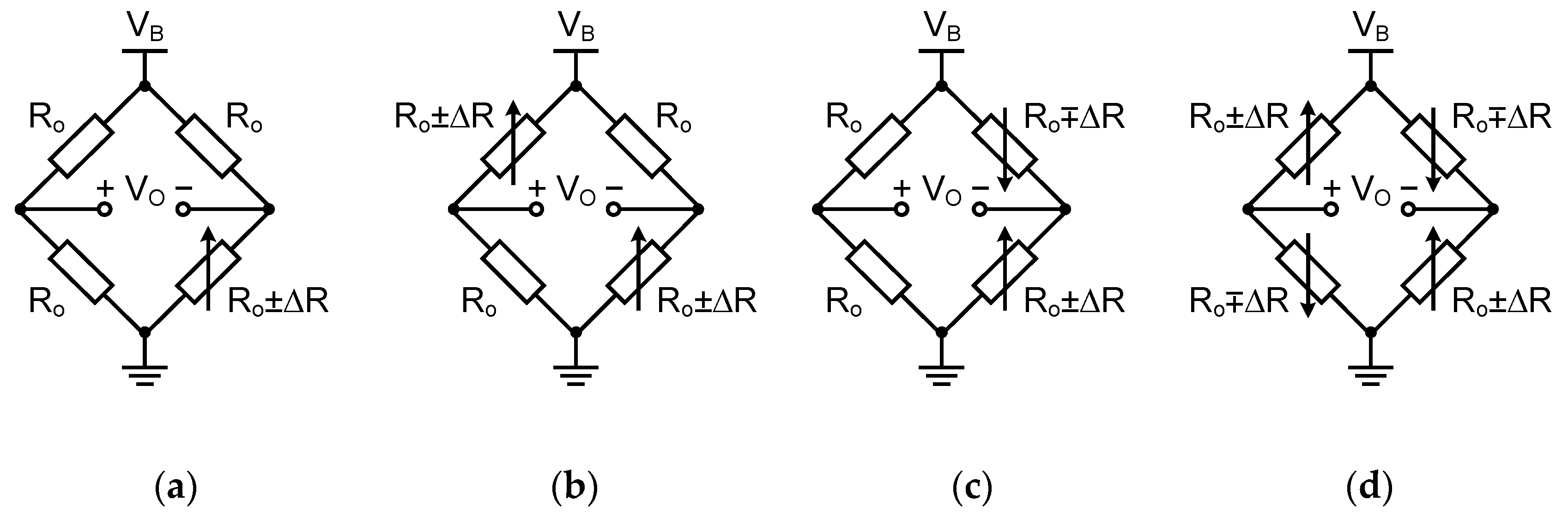
13]. A resistive sensor is implemented within the Wheatstone bridge structure; therein, it converts the resistance change into a voltage change. The structures of the Wheatstone bridge are voltage- and current-driven [
14]; the voltage-driven configuration is shown in
Figure 1. In addition, the output voltage and linearity error are listed in
Table 1. The current-driven configuration has the advantages of linearity and stability; however, the input sensitivity is proportional to the constant supply current. Therefore, the current-driven configuration is seldom used because it is difficult to accurately measure the change in the supply current.
The Wheatstone bridge readout integration circuits (ICs) primarily employ two conversion techniques [
11]. The first is a voltage-to-frequency converter that converts analog signals into the frequency domain [
15,
16,
17]. This scheme is simple in structure, but consumes considerable power and has a slow conversion rate over a wide operating range [
18]. The other technique is a voltage-to-digital converter that converts analog signals into digital signals [
19,
20]. The instrumentation amplifier (IA) is implemented to amplify small input signals, and an analog-to-digital converter (ADC) is required to convert the amplified signals to digital signals. Generally, the voltage-to-digital converter is more popular because of the well-established precision IA and ADC techniques. In the voltage-to-digital conversion, the IA is one of the key building blocks. A precision IA with low offset and low input referred noise is required because the offset and the input referred noise of the IA can generate a nonlinear output [
21]. Various techniques have been implemented for precision IAs, such as autozeroing and chopping, to secure microvolt offset levels [
22,
23,
24,
25,
26].
The autozeroing technique alleviates the offset and the flicker noise by sampling the offset and the low frequency flicker noise in the autozero capacitor in phase 1 (Φ1) and subtracting this information from the output voltage in phase 2 (Φ2). However, this technique generates switching noise due to sampling, and augments base band noise because of noise folding [
27].
The chopping technique fundamentally cancels the offset and flicker noise caused by the upmodulating offset and the low frequency flicker noise by chopping the frequency and passing the signal through a low pass filter (LPF). However, upmodulated offset and flicker noise create ripples, which must be attenuated by a ripple reduction loop (RRL). The RRL integrates the ripple generated by the chopping technique at the output stage and eliminates ripples through the negative feedback of this signal to the input stage. However, this process results in a notch at the chopper frequency of the transfer function of the operational amplifier. As a result, operational amplifiers implementing the chopping technique have a low unit-gain bandwidth (UGBW). Such a low UGBW is poorly-suited to many applications because it cannot deal with fast input signals. To avoid this drawback, in this paper, a chopper-stabilized multipath operational amplifier including a high frequency path (HFP) and a low frequency path (LFP) is implemented in the IA. In general, flicker noise is dominant in the low frequency region, so the chopping technique and RRL are employed to LFP but not HFP. Therefore, the transfer function of the LFP is limited to UGBW due to notch formation at the chopper frequency, but the HFP is not, so the transfer function of the multipath operational amplifier connecting LFP and HFP in parallel does not form the notch. Consequently, the multipath operational amplifier architecture resolves the shortcoming of having a low UGBW, and has the merit of being appropriate for a variety of applications.
A small input signal is amplified by the three-operational amplifier IA, having high input impedance, excellent linearity, and adjustable gain; the amplified signal is then converted into a digital signal via a 12-bit successive approximation register (SAR) ADC.
This paper is organized as follows.
Section 2 explains the topology of the proposed Wheatstone bridge readout IC with a chopper-stabilized multipath operational amplifier. The experimental results are described in
Section 3. A discussion and conclusions are presented in
Section 4 and
Section 5, respectively.
2. Proposed Wheatstone Bridge Readout IC with Chopper-Stabilized Multipath Operational Amplifier
This section discusses a proposed Wheatstone bridge readout IC with a chopper-stabilized multipath operational amplifier.
Section 2.1 discusses the top architecture and subblocks of the Wheatstone bridge readout IC.
Section 2.2 explains the schematic and operating principles of a chopper-stabilized multipath operational amplifier applied as a single-ended amplifier in a three-operational amplifier IA.
2.1. Top Architecture of the Wheatstone Bridge Readout IC
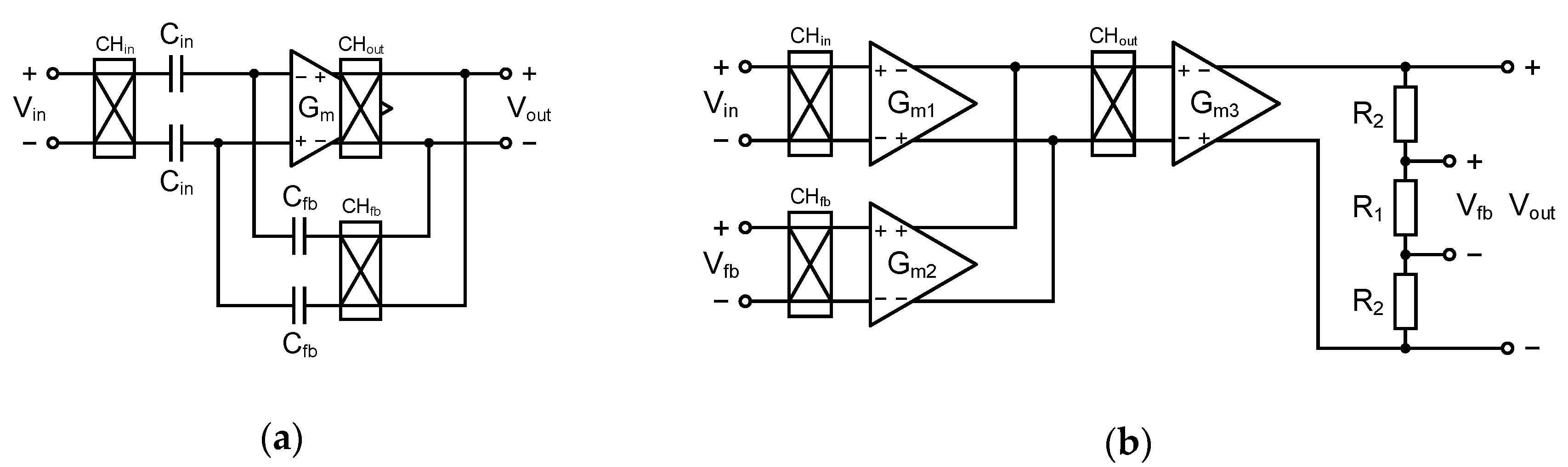
Various types of IAs that can be implemented to properly amplify small input signals; capacitively coupled IAs (CCIAs), current feedback IAs (CFIAs), and three-operational amplifier IAs are the most popular types. The conventional architecture of CCIAs is shown in
Figure 2a; the output voltage is given as
The CCIA has high power efficiency, but the input stage is composed of capacitors, so the input impedance is lower than other IAs. To solve this issue, a circuit that can increase the input impedance, such as a positive feedback loop (PFL), is required [
28].
The CFIA has high input impedance, but gain accuracy is limited by a mismatch between the input and the feedback transconductance [
28]. A block diagram of the CFIA is shown in
Figure 2b, and the output voltage is expressed as
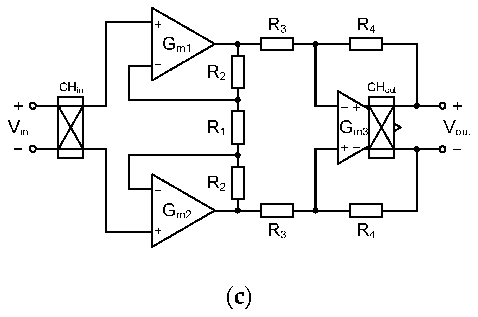
The three-operational amplifier IA has low power efficiency owing to the use of two low-noise input amplifiers, but achieves high input impedance and excellent linearity. The conventional block diagram of the three-operational amplifier IA is shown in
Figure 2c.
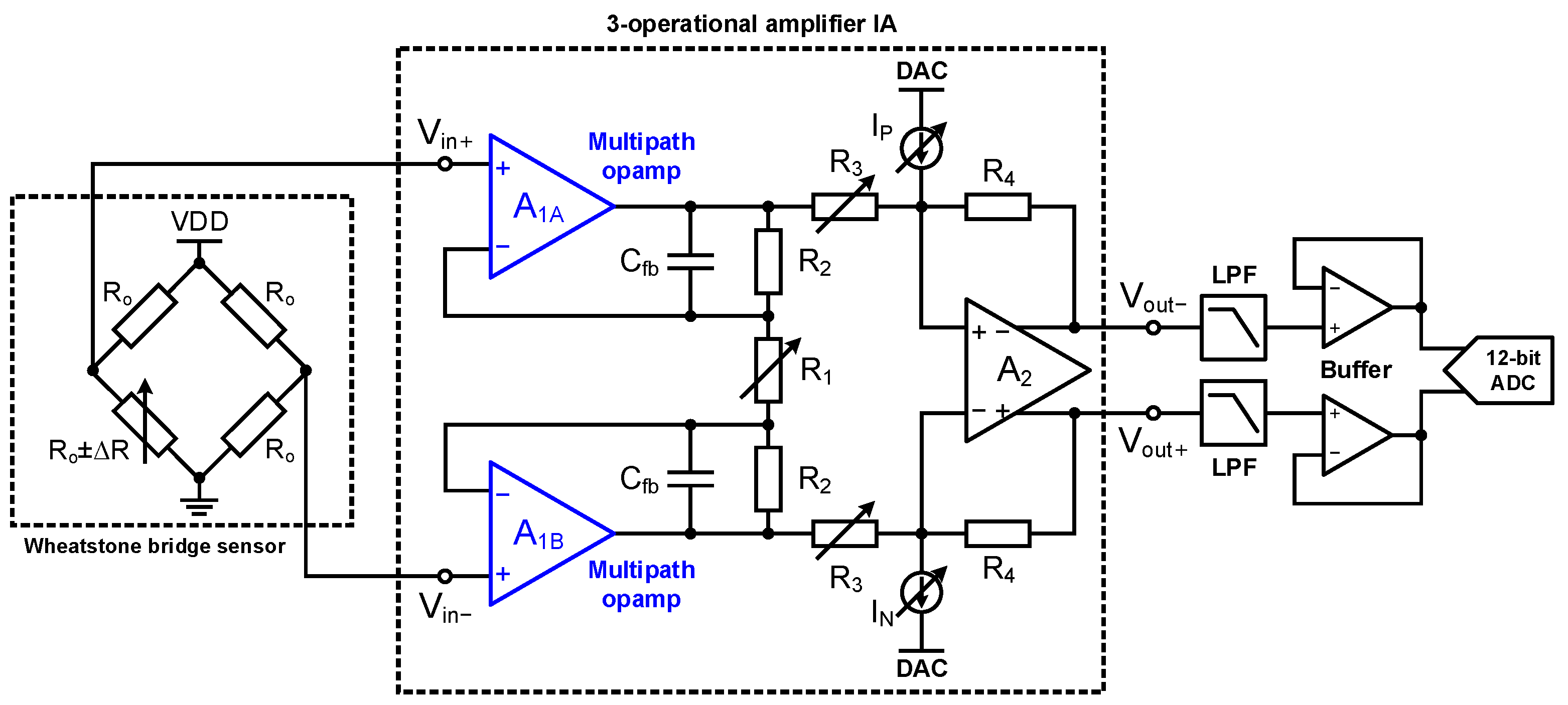
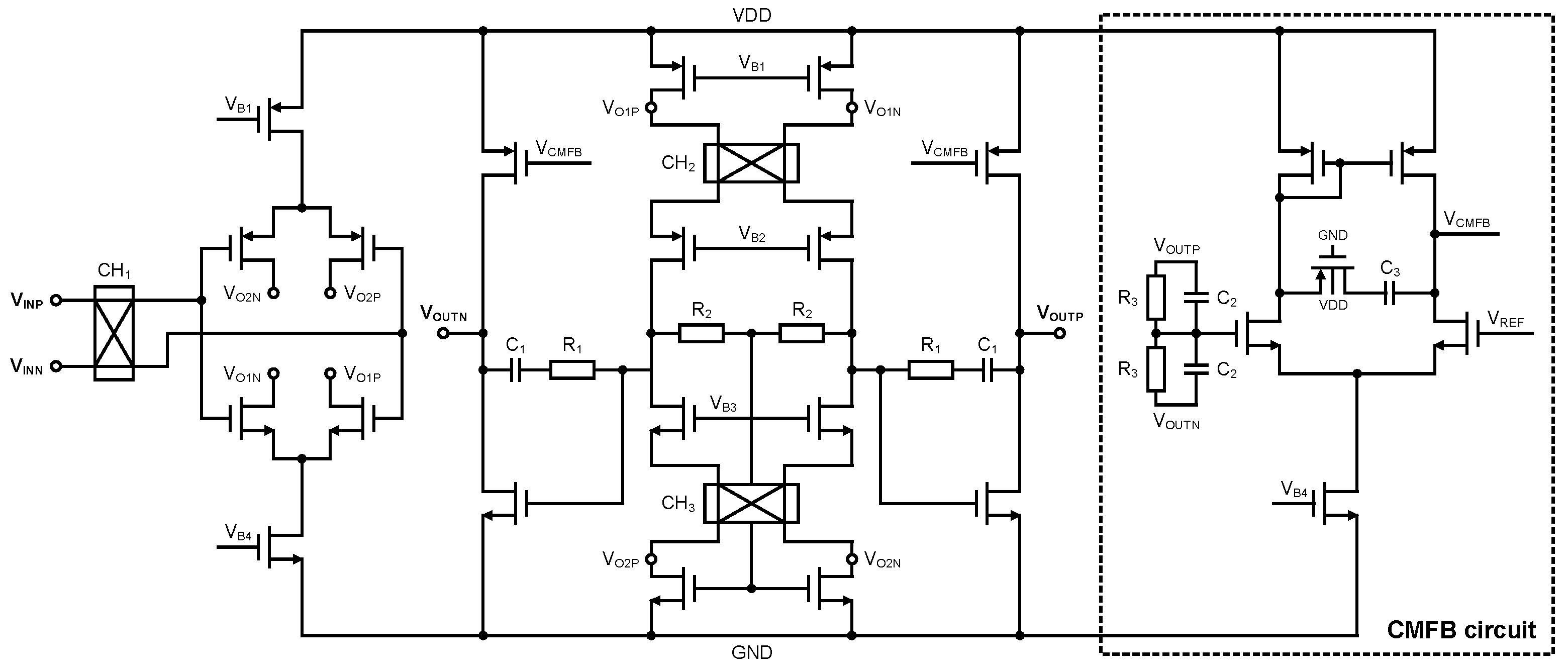
In this paper, we implement the three-operational amplifier IA architecture to acquire excellent linearity and a comfortably adjustable gain. The top architecture of the proposed Wheatstone bridge readout IC, including the three-operational amplifier IA, is shown in
Figure 3. The output offset of the three-operational amplifier IA is adjustable using a digital-to-analog converter (DAC) connected to the input of the fully-differential amplifier A
2. The transfer function of the three-operational amplifier IA, including the DAC operation, is expressed as
The structure of the Wheatstone bridge sensor is simulated by a single-element varying structure; the variable resistance is modeled using Verilog-A. The proposed three-operational amplifier IA is comprised of a first stage, consisting of A
1A and A
1B, and a second stage, consisting of A
2. The gain of each stage is determined by the variable resistors, R
1 and R
3. These resistors are designed as 5-bit programmable resistors. The two single-ended amplifiers A
1A and A
1B at the input stage produce low noise by using the proposed chopper-stabilized multipath operational amplifier, consisting of an HFP and LFP. In addition, the fully-differential amplifier A
2 applies the chopping technique; its schematic is shown in
Figure 4. Chopping is applied at the input stage and at the folded cascode stage of the fully-differential amplifier. The input range is extended by employing the rail-to-rail input stage.
The output of the three-operational amplifier IA, which amplifies the input small signal, passes through the LPF and buffer, and is then converted into a digital signal by a 12-bit SAR ADC. The LPF adopts a Sallen-key topology, and the simulation results indicate that the cutoff frequency is 840 Hz. The 12-bit SAR ADC employs a resistor–capacitor hybrid structure that diminishes the area by 16 times compared to a capacitor-only DAC. An offset calibration technique is implemented for the comparator in the 12-bit SAR ADC to achieve high linearity and low offset.
2.2. Architecture and Circuit Implementation of a Chopper-Stabilized Multipath Operational Amplifier
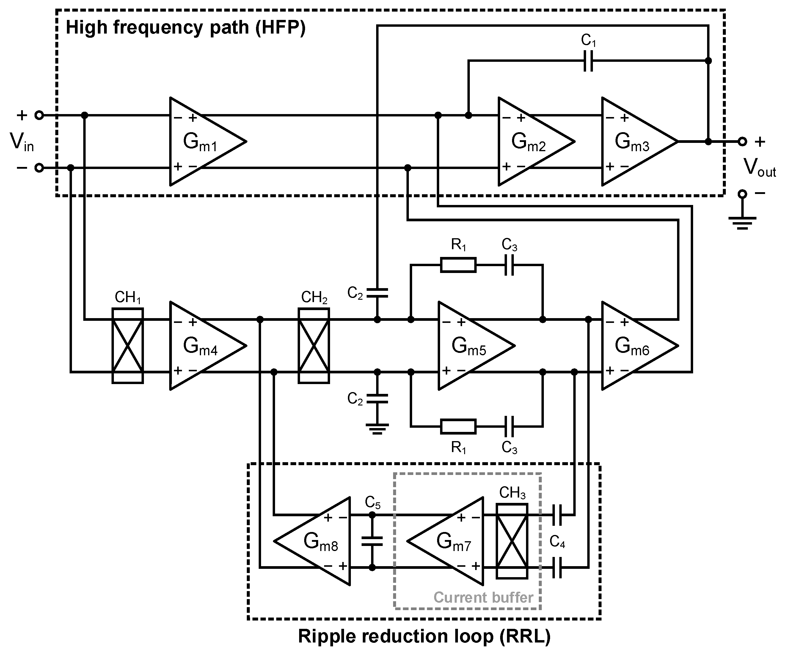
A block diagram of the proposed chopper-stabilized multipath operational amplifier is shown in
Figure 5. First, a high frequency bypass technique is applied by a wide bandwidth and high gain amplifier composed of G
m1, G
m2, and G
m3, and nested Miller compensation is accomplished on the HFP by C
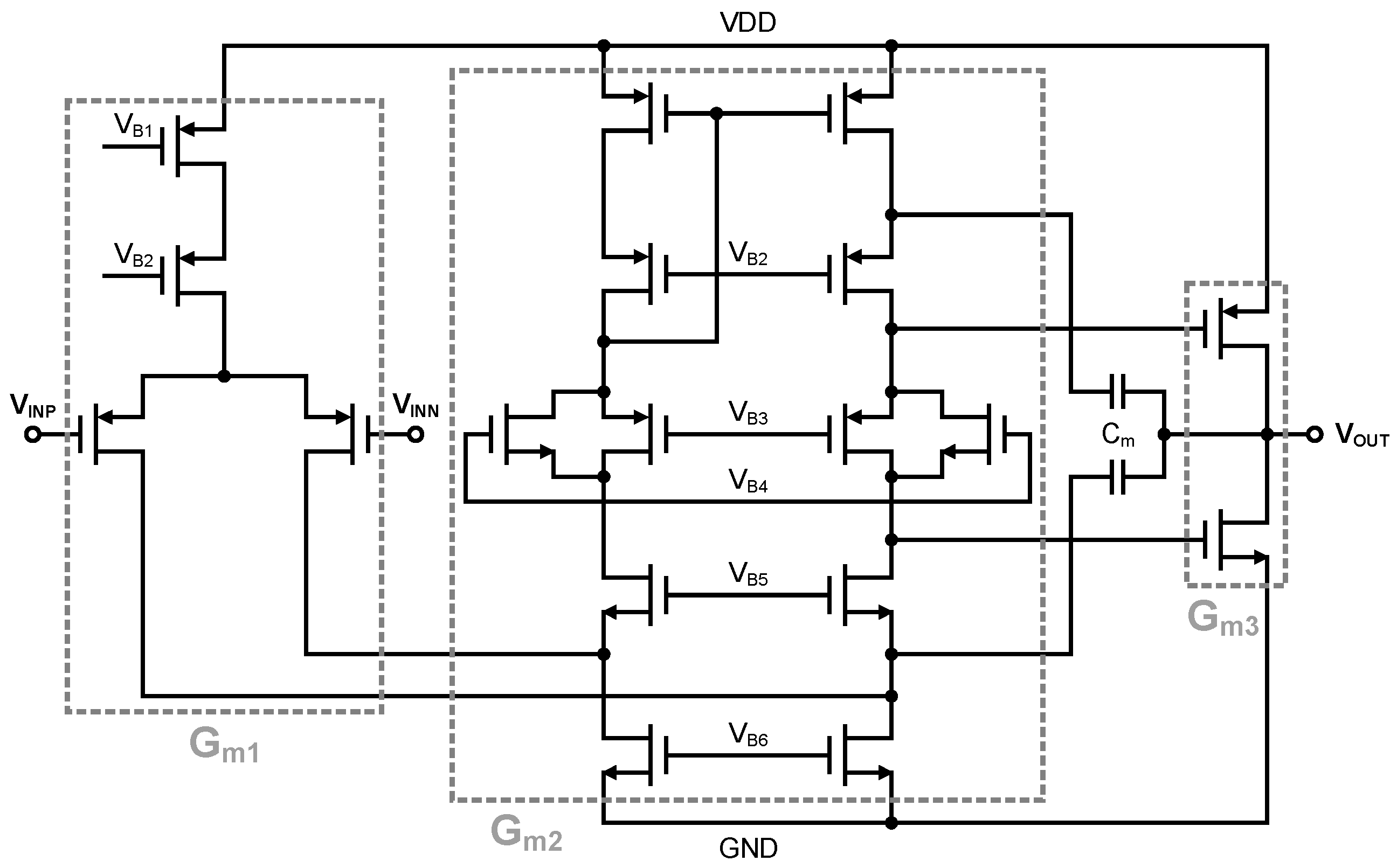
1. The HFP circuit implements a PMOS input stage and enhances power efficiency and slew rate by adopting Monticelli-based class-AB output stages, as shown in
Figure 6. The LFP consists of G
m4, G
m5, and G
m6, and choppers CH
1 and CH
2 are used to apply the chopping technique.
The low frequency input signal is modulated into the high frequency region through CH
1, is then demodulated back to the low frequency region by CH
2, and passes through an integrator consisting of G
m5 and C
3. On the other hand, the low frequency flicker noise and offset of the G
m4 input are modulated into the high frequency region by CH
2 and are attenuated by the integrator. Using this technique, the offset component modulated into the high frequency region gives rise to ripple, so an RRL is implemented to reduce it. The RRL input is AC-coupled and consists of a current buffer, C
5, and G
m8. The RRL perceives the ripple at the output of G
m5 and converts it to DC current. This DC current compensates for the offset current of the G
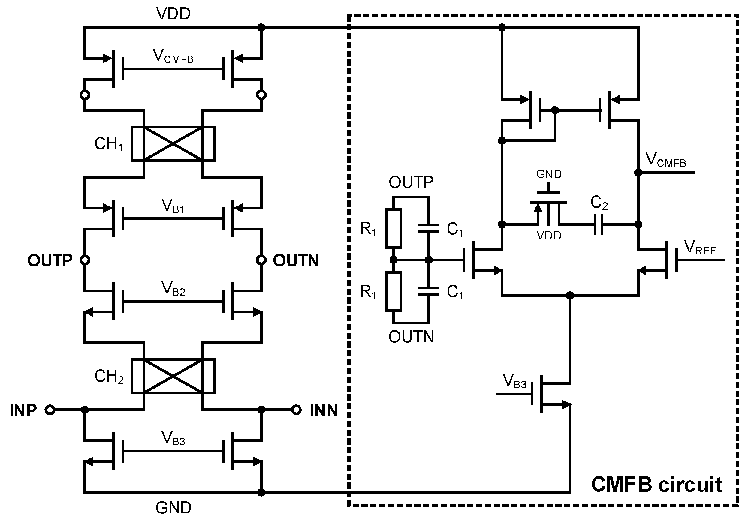
m4, which eliminates the ripple. A schematic of the current buffer containing the chopper in the RRL is shown in
Figure 7.
3. Measurement Results of Proposed Wheatstone Bridge Readout IC
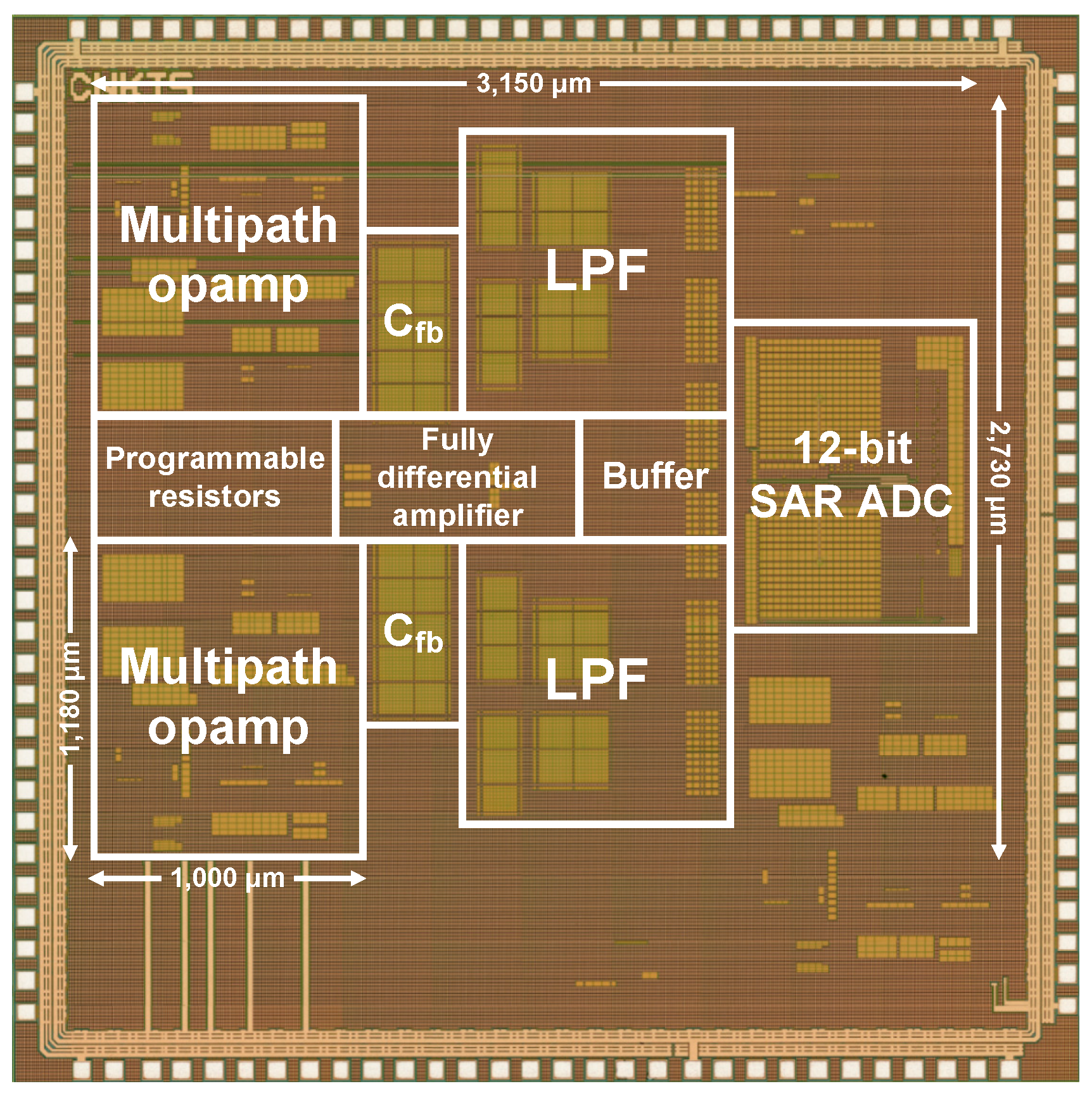
The proposed Wheatstone bridge readout IC is manufactured using a 0.18 µm one polysilicon and six metal layers (1P6M) complementary metal-oxide-semiconductor (CMOS) process. A chip microphotograph of the proposed Wheatstone bridge readout IC is shown in
Figure 8. The fabricated chopper-stabilized multipath operational amplifier has an area of 1.18 mm
2, while the area of the Wheatstone bridge readout IC with three-operational amplifier IA, LPF, buffer, and 12-bit SAR ADC is 8.6 mm
2.
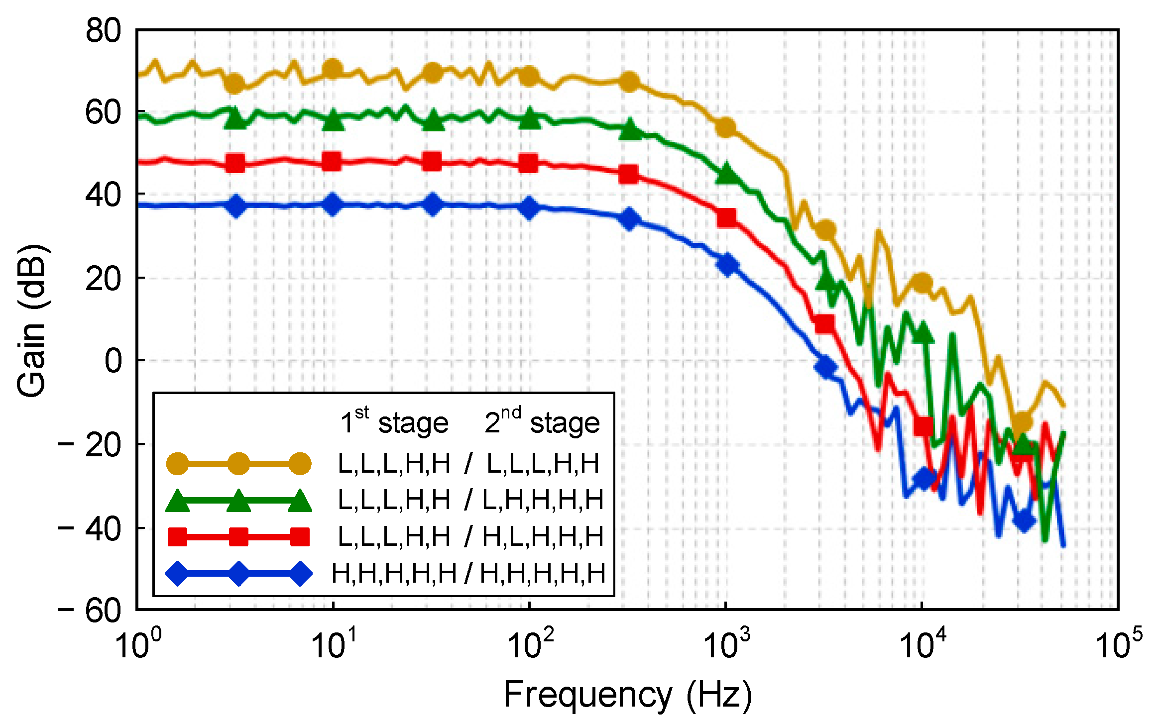
Figure 9 shows the transfer functions of the three-operational amplifier IA using various 5-bit programmable resistor settings; a gain adjustment of approximately 38–70 dB is possible. The gain of the three-operational amplifier IA is adjusted in inverse proportion to R
1 and R
3 according to Equation (3). The resistances of R
1 and R
3 are at their maximum (835 kΩ) when the 5-bit register bits are all set to high, and are at their minimum (26 kΩ) when all register bits are set to low. As a result, the three-operational amplifier IA has a gain of 38 dB when the registers controlling R
1 and R
3 are high, and 70 dB when these are set to L, L, L, H, H. For each register setting, we can compare the gain calculated by Equation (3) with the measured gain; these results are shown in
Table 2. As a result of the comparison, there are some errors of gain. These errors are expected to be caused by the layout stage and mismatch. These 5-bit programmable resistors must be properly adjusted for the range of the input voltages. The input range for this Wheatstone bridge readout IC is ±20 mV.
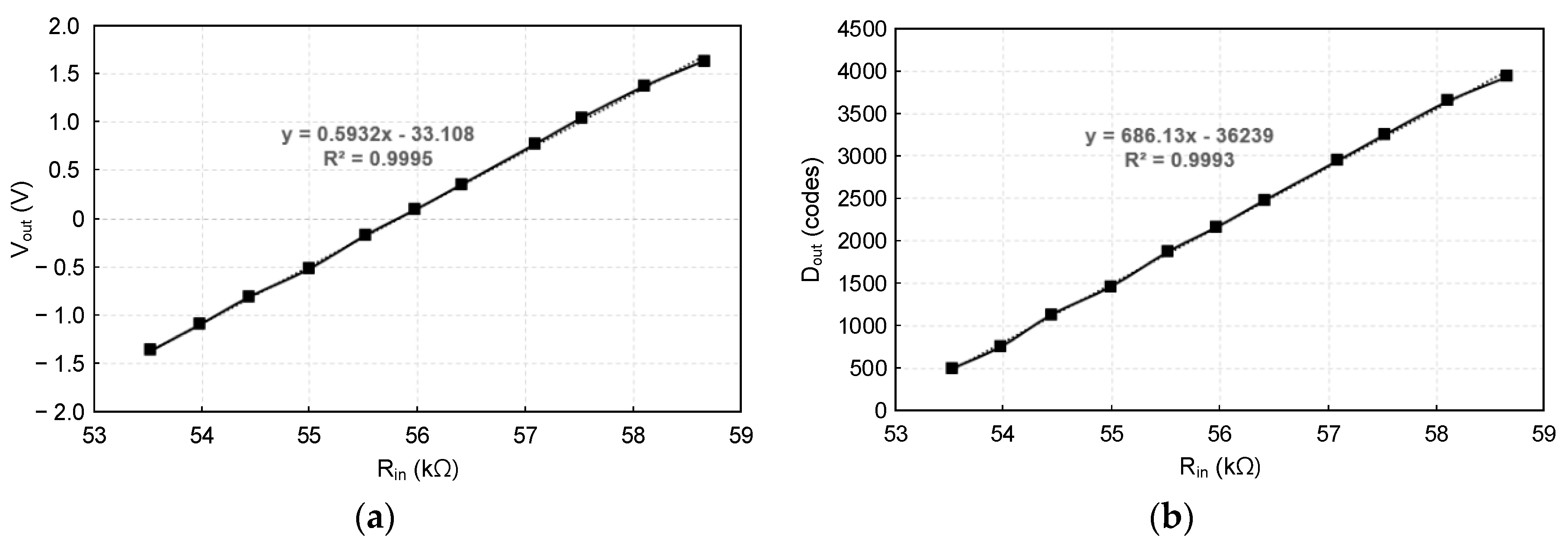
Figure 10 shows the output voltage and digital code output of the Wheatstone bridge readout IC based on input resistance. The input resistance range is 53.5–58.5 kΩ, and the coefficient for the determination of the output voltage trend line is 0.9995 according to
Figure 10a. Finally, the coefficient for the determination of the output digital code trend line is 0.9993 according to
Figure 10b. In addition, the R
o resistance of the Wheatstone bridge is 56 kΩ, and the input resistance range is a ±20 mV based on input voltage range. Since the minimum gain of the proposed Wheatstone bridge readout IC is 37.53 dB (75.25 times) and the supply voltage is 1.8 V, the maximum input voltage range can be calculated as approximately 24 mV, which is the value divided by 1.8 V by 75.25. However, in this research, the maximum input voltage range was set to 20 mV because the proposed Wheatstone bridge readout IC may not operate normally near the minimum and maximum supply voltages. The input resistance range varies with the R
o resistance of the Wheatstone bridge, and the voltage difference at the differential output of the Wheatstone bridge cannot exceed the input voltage range. This input voltage range changes with the gain adjustment of the Wheatstone bridge readout IC, and the resolution of the output signal is maintained. Since the input voltage range is adjustable, it can be applied to sensors with more various specifications. Measurement results show that the differential output voltage range of the Wheatstone bridge readout IC is −1.36 V to 1.63 V at a 1.8 V supply voltage.
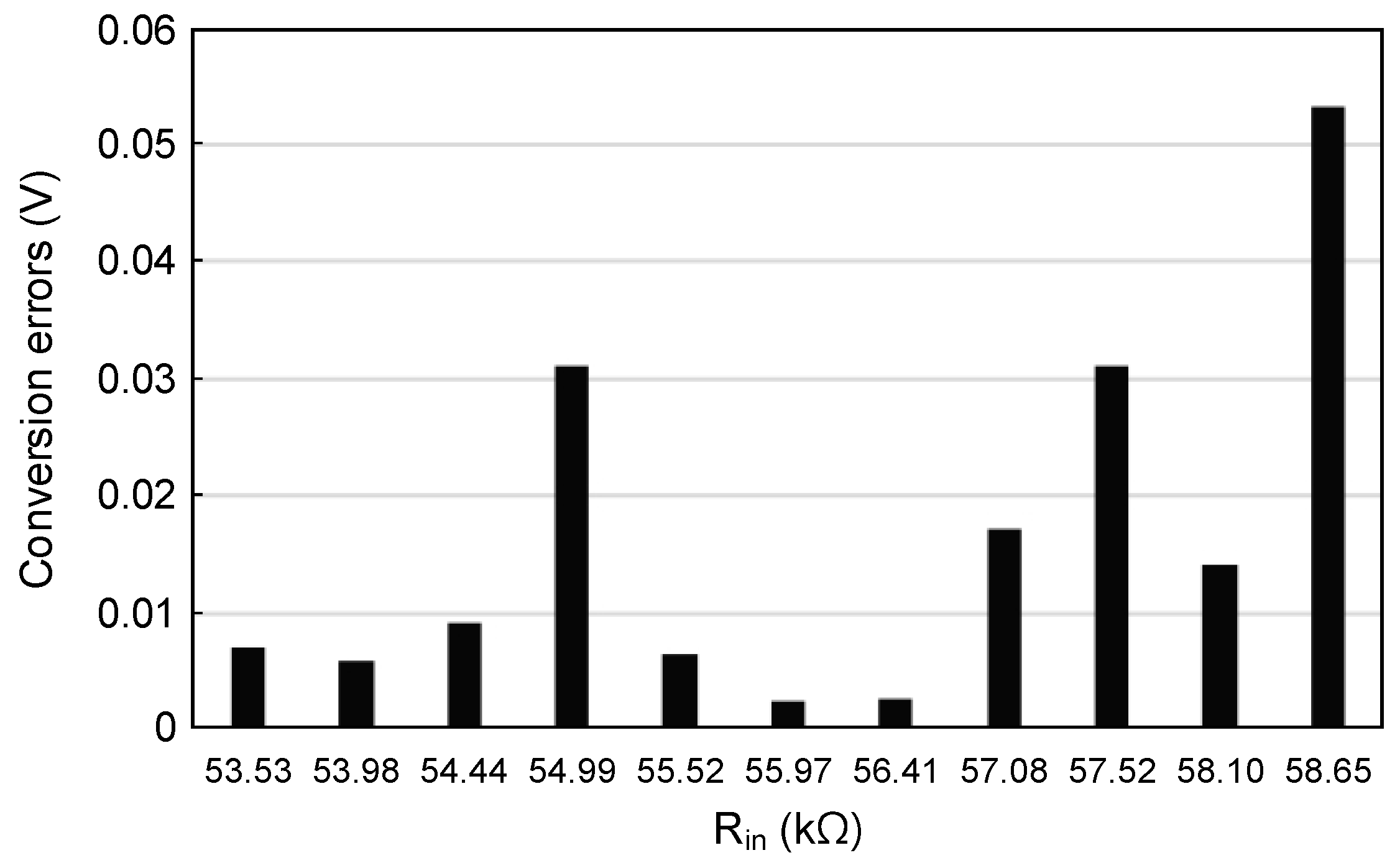
Figure 11 shows the conversion error of the measured output voltage. The conversion error is a comparison of the ideal output voltage value calculated as a primary function and the measured output voltage value. If the conversion error is large, the linearity of the Wheatstone bridge readout IC is reduced. Referring to
Figure 11, the conversion error boosts as the input resistance increases, which is analyzed, as the output voltage is too near to the supply voltage and the linearity of the operational amplifier is diminished. To solve this issue, a slight reduction in the gain of the Wheatstone bridge readout IC can be applied to adjust the output voltage so that it is not close to the supply voltage.
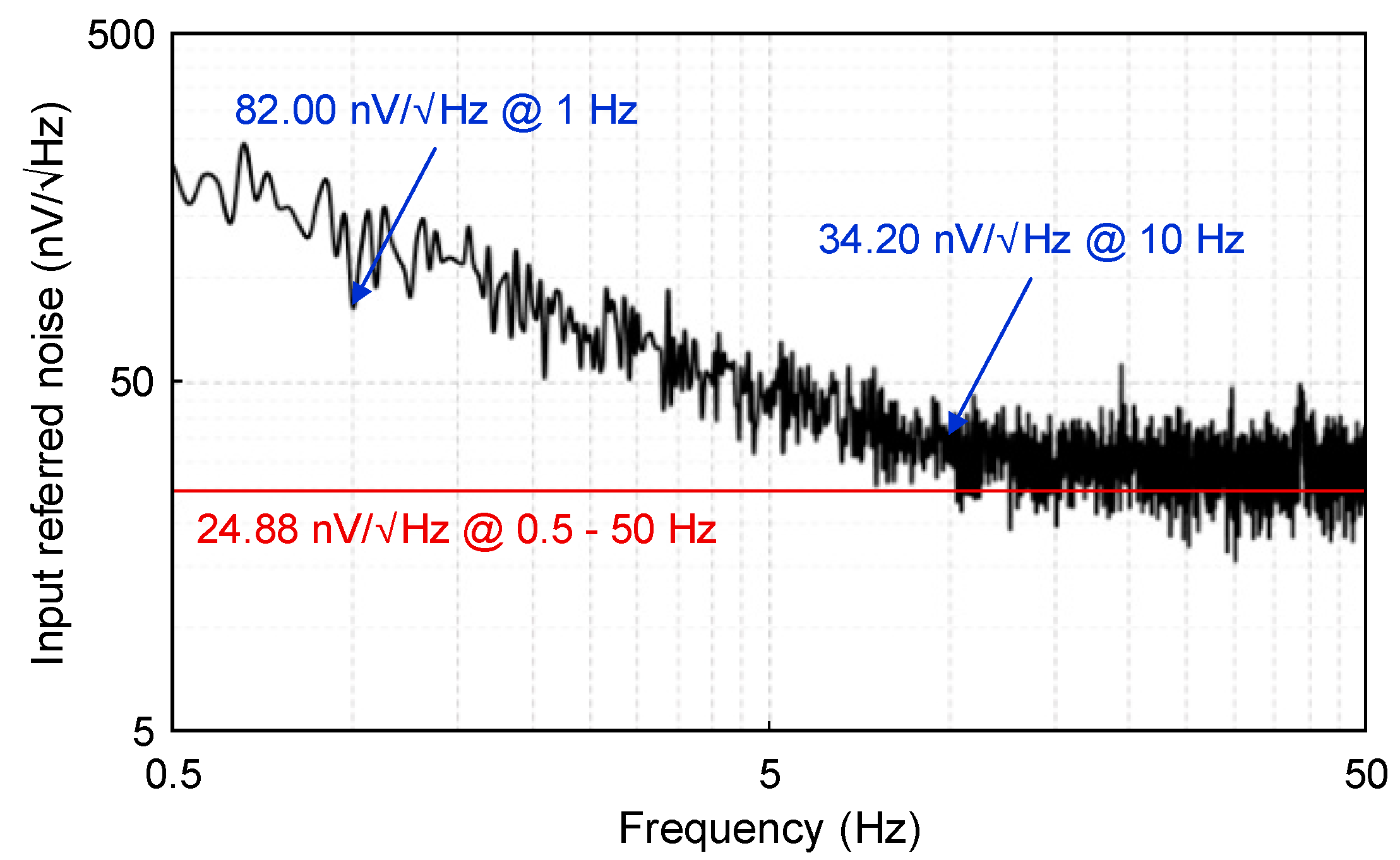
Figure 12 shows the measured input referred noise of the Wheatstone bridge readout IC. Chopping techniques are implemented twice in the LFP of the chopper-stabilized multipath operational amplifiers and fully-differential amplifiers. The measured input referred noise is 82.00 nV/√Hz at 1 Hz and 34.20 nV/√Hz at 10 Hz, and the input noise voltage density is 24.88 nV/√Hz over the 0.5–50 Hz range.
In
Table 3, the performance of the Wheatstone bridge readout IC is summarized and compared with several state-of-the-art three-operational amplifier IAs. The proposed Wheatstone bridge readout IC has the advantage of high current consumption, but low input referred noise compared with other studies. If the input referred noise is large, the noise can be amplified by the three-operational amplifier IA, which affects the precision of the output signal. Consequently, the larger the input referred noise, the greater the noise is on the output stage, which can be fatal to the linearity of the Wheatstone bridge readout IC. Generally, however, there is a trade-off between the method of reducing input referred noise and the method of decreasing current. Additionally, the chopping technique is implemented to reduce input referred noise. Compared with other studies, RRL is added to eliminate the ripple caused by the chopping technique; this is designed to adjust the gain of the three-operational amplifier IA.
4. Discussion
Recently, the demand for Wheatstone bridge readout ICs has grown for various sensor applications. Because the input resistance change of a Wheatstone bridge sensor is generally small, the change of the converted voltage signal also has a small value. As a result, low noise IAs that can accurately amplify small input voltage changes is an active research area. Chopping and autozeroing are mainly implemented for low noise IAs, and there are various types of IAs, such as three-operational amplifier IAs, CCIAs, and CFIAs. In this paper, the three-operational amplifier IA structure is implemented to easily acquire high input impedance and adjustable gain; however, CCIAs and CFIAs also have certain advantages, so further research is required regarding these. In addition, the fabricated chopper-stabilized multipath operational amplifier must consume a significant amount of current to provide the low noise characteristics. Consequently, the power consumption of Wheatstone bridge readout ICs has increased significantly, and measures to reduce it are needed. The following are potential ways to reduce power consumption: The first method is to lessen the power consumption of the operational amplifier itself. This can be done by altering the size and bias voltage of the devices in the amplifier. However, because the size of the device is directly related to the noise component, it must be adjusted appropriately to avoid a significant increase in input referred noise. The second method is to diminish the power dissipation in LPF, buffer, etc. in addition to the operational amplifier. For instance, if the resistors of the LPF are replaced with a switched capacitor architecture, the cutoff frequency may not be obvious, but it has the advantage that power consumption is considerably decreased. Additionally, eliminating the buffer implemented for monitoring can cut power consumption. These methods can reduce the power consumption of the proposed Wheatstone bridge readout IC, but further discussion of them will be required in the future.
5. Conclusions
In this paper, we propose a Wheatstone bridge readout IC with chopper-stabilized multipath operational amplifier. The proposed Wheatstone bridge readout IC is fabricated using a standard 0.18 µm 1P6M CMOS process and has an area of 8.6 mm2. It dissipates 1.5 mW of power using a 1.8 V supply voltage. The proposed Wheatstone bridge readout ICs consist of a three-operational amplifier IA, LPF, buffer, and 12-bit SAR ADC. The three-operational amplifier IA achieves a gain of 38–70 dB using two 5-bit programmable resistors. The chopper-stabilized multipath operational amplifier, which forms the input stage of the three-operational amplifier IA, consists of an HFP and an LFP with a chopping technique applied to reduce noise. In addition, a RRL is implemented to effectively attenuate the ripple generated by chopping in the LFP. The input noise voltage density of the proposed Wheatstone bridge readout IC was shown to be 24.88 nV/√Hz over the 0.5–50 Hz range and the input range was ±20 mV.
Author Contributions
Conceptualization and supervision, H.K. (Hyoungho Ko); validation, J.L.; investigation and writing—original draft preparation, K.H.; writing—review and editing, H.K. (Hyungseup Kim), J.K., D.Y., H.H., and Y.K. All authors have read and agreed to the published version of the manuscript.
Funding
This research was supported by a grant to Bio-Mimetic Robot Research Center Funded by Defense Acquisition Program Administration, and by Agency for Defense Development (UD190018ID).
Acknowledgments
The chip fabrication and EDA tool were supported by the IC Design Education Center (IDEC), Republic of Korea.
Conflicts of Interest
The authors declare no conflict of interest.
References
- Maruyama, M.; Taguchi, S.; Yamanoue, M.; Iizuka, K. An Analog Front-End for a Multifunction Sensor Employing a Weak-Inversion Biasing Technique with 26 nVrms, 25 aCrms, and 19 fArms Input-Referred Noise. IEEE J. Solid-State Circuits 2016, 51, 2252–2261. [Google Scholar] [CrossRef]
- Wu, R.; Chae, Y.; Huijsing, J.; Makinwa, K.A.A. A 20-b±40-mV Range Read-Out IC With 50-nV Offset and 0.04% Gain Error for Bridge Transducers. IEEE J. Solid-State Circuits 2012, 47, 2152–2163. [Google Scholar] [CrossRef]
- Jun, J.; Rhee, C.; Kim, M.; Kang, J.; Kim, S. A 21.8b sub-100μHz 1/f corner 2.4μV-offset programmable-gain read-out IC for bridge measurement systems. In Proceedings of the IEEE International Solid-State Circuits Conference, San Francisco, CA, USA, 11–15 February 2018; pp. 330–332. [Google Scholar] [CrossRef]
- Ezekwe, C.D.; Vanderhaegen, J.P.; Xing, X.; Balachandran, G.K. A 6.7nV/√Hz Sub-mHz-1/f-corner 14b analog-to-digital interface for rail-to-rail precision voltage sensing. In Proceedings of the IEEE International Solid-State Circuits Conference, San Francisco, CA, USA, 20–24 February 2011; p. 246. [Google Scholar] [CrossRef]
- Tu, C.-C.; Wang, Y.-K.; Lin, T.-H. A 0.06mm2± 50mV range −82dB THD chopper VCO-based sensor readout circuit in 40 nm CMOS. In Proceedings of the Symposium on VLSI Circuits, Kyoto, Japan, 5–8 June 2017; pp. C84–C85. [Google Scholar] [CrossRef]
- Pan, S.; Jiang, H.; Makinwa, K.A.A. A CMOS temperature sensor with a 49fJK2resolution FoM. In Proceedings of the Symposium on VLSI Circuits, Kyoto, Japan, 5–8 June 2017; pp. C82–C83. [Google Scholar] [CrossRef]
- Ferri, G.; Stornelli, V.; De Marcellis, A.; Flammini, A.; Depari, A. Novel CMOS fully integrable interface for wide-range resistive sensor arrays with parasitic capacitance estimation. Sens. Actuators B 2008, 130, 207–215. [Google Scholar] [CrossRef]
- Ferri, G.; De Marcellis, A.; Di Carlo, C.; Stornelli, V.; Flammini, A.; Depari, A.; Marioli, D.; Sisinni, E. A CCII-Based Low-Voltage Low-Power Read-Out Circuit for DC-Excited Resistive Gas Sensors. IEEE Sens. J. 2009, 9, 2035–3041. [Google Scholar] [CrossRef]
- Aguilar, R.N.; Meijer, G.C.M. Fast interface electronics for a resistive touch-screen. In Proceedings of the IEEE Sensors, Orlando, FL, USA, 12–14 June 2002; pp. 1360–1363. [Google Scholar] [CrossRef]
- Jiang, H.; Makinwa, K.A.; Nihtianov, S. An Energy-Efficient 3.7-nV/√Hz Bridge Readout IC with a Stable Bridge Offset Compensation Scheme. IEEE J. Solid-State Circuits 2018, 54, 856–864. [Google Scholar] [CrossRef]
- Koay, K.C.; Chan, P.K. A Low Energy-Noise 65 nm CMOS Switched-Capacitor Resistive-Bridge Sensor Interface. IEEE Trans. Circuits Syst. I Regul. Pap. 2016, 64, 799–810. [Google Scholar] [CrossRef]
- Stefanescu, D.M. Handbook of Force Transducers: Principles and Components, 1st ed.; Springer Science & Business Media: Berlin/Heidelberg, Germany, 2011; pp. 49–68. [Google Scholar]
- Fraden, J. Handbook of Modern Sensors: Physics, Designs, and Applications, 3rd ed.; Springer Science & Business Media: Berlin/Heidelberg, Germany, 2004; pp. 59–65. [Google Scholar]
- Thanachayanont, A.; Sangtong, S. Low-Voltage Current-Sensing CMOS Interface Circuit for Piezo-Resistive Pressure Sensor. ETRI J. 2007, 29, 70–78. [Google Scholar] [CrossRef]
- Ferrari, V.; Marioli, D.; Taroni, A. Oscillator-based interface for measurand-plus-temperature readout from resistive bridge sensors. IEEE Trans. Instrum. Meas. 2000, 49, 585–590. [Google Scholar] [CrossRef]
- Ferrari, V.; Ghisla, A.; Vajna, Z.K.; Marioli, D.; Taroni, A. ASIC front-end interface with frequency and duty cycle output for resistive-bridge sensors. Sens. Actuators A 2007, 138, 112–119. [Google Scholar] [CrossRef]
- Grassi, M.; Malcovati, P.; Baschirotto, A. A 141-dB Dynamic Range CMOS Gas-Sensor Interface Circuit without Calibration with 16-Bit Digital Output Word. IEEE J. Solid-State Circuits 2007, 42, 1543–1554. [Google Scholar] [CrossRef]
- Ong, G.T.; Chan, P.K. A Power-Aware Chopper-Stabilized Instrumentation Amplifier for Resistive Wheatstone Bridge Sensors. IEEE Trans. Instrum. Meas. 2014, 63, 2253–2263. [Google Scholar] [CrossRef]
- Wu, R.; Huijsing, J.H.; Makinwa, K.A.A. A 21b ±40mV range read-out IC for bridge transducers. In Proceedings of the IEEE International Solid-State Circuits Conference, San Francisco, CA, USA, 20–24 February 2011; pp. 110–112. [Google Scholar] [CrossRef]
- Ko, H.; Kim, H.; Lee, B.; Kim, J.; Cho, D.D.; Han, K. Low-noise Analog Front-end with Chopper-stabilized Multipath Current-feedback Instrumentation Amplifier for Resistive Sensors. Sens. Mater. 2019, 31, 1697–1706. [Google Scholar] [CrossRef]
- Fan, Q.; Huijsing, J.H.; Makinwa, K.A.A. A 21 nV/√Hz Chopper-Stabilized Multi-Path Current-Feedback Instrumentation Amplifier with 2μV Offset. IEEE J. Solid-State Circuits 2011, 47, 464–475. [Google Scholar] [CrossRef]
- Witte, J.F.; Huijsing, J.H.; Makinwa, K.A.A. A chopper and auto-zero offset-stabilized CMOS instrumentation amplifier. In Proceedings of the Symposium on VLSI Circuits, Kyoto, Japan, 16–18 June 2009; pp. 210–211. [Google Scholar]
- Pertijs, M.A.P.; Kindt, W.J. A 140 dB-CMRR Current-Feedback Instrumentation Amplifier Employing Ping-Pong Auto-Zeroing and Chopping. IEEE J. Solid-State Circuits 2010, 45, 2044–2056. [Google Scholar] [CrossRef]
- Wu, R.; Makinwa, K.A.A.; Huijsing, J.H. A Chopper Current-Feedback Instrumentation Amplifier with a 1 mHz 1/f Noise Corner and an AC-Coupled Ripple Reduction Loop. IEEE J. Solid-State Circuits 2009, 44, 3232–3243. [Google Scholar] [CrossRef]
- Witte, J.F.; Makinwa, K.A.A.; Huijsing, J.H. A CMOS Chopper Offset-Stabilized Opamp. IEEE J. Solid-State Circuits 2007, 42, 1529–1535. [Google Scholar] [CrossRef]
- Belloni, M.; Bonizzoni, E.; Fornasari, A.; Maloberti, F. A Micropower Chopper—CDS Operational Amplifier. IEEE J. Solid-State Circuits 2010, 45, 2521–2529. [Google Scholar] [CrossRef]
- Enz, C.C.; Temes, G.C. Circuit techniques for reducing the effects of op-amp imperfections: Autozeroing, correlated double sampling, and chopper stabilization. Proc. IEEE 1996, 84, 1584–1614. [Google Scholar] [CrossRef]
- Fan, Q.; Sebastiano, F.; Huijsing, H.; Makinwa, K. A 1.8μW 60 nV/√Hz Capacitively-Coupled Chopper Instrumentation Amplifier in 65 nm CMOS for Wireless Sensor Nodes. IEEE J. Solid-State Circuits 2011, 46, 1534–1543. [Google Scholar] [CrossRef]
- Yen, C.-J.; Chung, W.-Y.; Chi, M.C. Micro-power low-offset instrumentation amplifier IC design for biomedical system applications. IEEE Trans. Circuits Syst. I Regul. Pap. 2004, 51, 691–699. [Google Scholar] [CrossRef]
© 2020 by the authors. Licensee MDPI, Basel, Switzerland. This article is an open access article distributed under the terms and conditions of the Creative Commons Attribution (CC BY) license (http://creativecommons.org/licenses/by/4.0/).

 ,
, 


