Abstract
In the last decade, the application of metamaterials has become a very interesting way of implementing passive devices in microwave, terahertz, and optical frequency ranges. Up until now, selective filters, absorbers, polarizers, and lenses have been designed and constructed using these artificial materials, simultaneously showing the possibility for many other potential applications. Because of the simplified fabrication process, in particular, planar structures called metasurfaces (MS), are developing very fast. In the literature, there are many studies on the properties of various metasurfaces, but there are a lack of papers related to the analysis of the impact of structure deformations on their properties. In this paper, three commonly utilized structures of metasurfaces were designed for the same resonant frequency and on the same substrate. The numerical models were built and verified using the measurements of fabricated structures. During the experiment, the geometrical parameters of the metasurface cells were swept and a mechanical in-plane deformation in orthogonal directions was applied to the examined structures. Finally, sensitivity to the geometry distortions of the analyzed structures was evaluated and discussed.
1. Introduction
Metamaterials (MM) have been known about since the mid-twentieth century, but their rapid development has been observed in the last decade. A metamaterial is an artificial, man-made structure consisting of periodic or quasi-periodic arrays of sub-wavelength size unit elements that can take on the properties of non-naturally occurring materials, for example, a negative refractive index or both negative permittivity and permeability, referred to as double-negative structures (DNG) [1,2,3,4,5]. This allows for new opportunities to interact with the electromagnetic waves. Various field transformations of arbitrary incident fields can be achieved [6]. Metamaterials and their planar versions (metasurfaces (MS)) can potentially find applications in telecommunications [7,8], measuring systems [9,10], selective absorbing structures [11,12,13,14], polarizers [6,15,16], surface wave control devices [6], and imaging systems (for lensing electromagnetic waves) [17,18,19], or in many others that we do not know yet.
Unit elements can be conductive or dielectric. The geometry and size of the unit element, as well as the distance between the elements in the array and the properties of the dielectric substrate can affect the way of interaction with an electromagnetic wave. In the literature, one can find a lot of works on the analysis of the operation, design, and synthesis of various meta-surface structures, where individual unit cells are analyzed, and for which frequency characteristics, formulas for resonance frequencies or equivalent schemes are determined [8,16]. An evaluation of the selected metasurface’s sensitivity to the distortion of its geometry caused, for example, by improper production processes or services, is an important task. Metasurfaces that are less sensitive to deformation or other changes in geometry can be used in existing applications (filters, polarizers, or absorbers), especially where various types of deformation may occur. In contrast, metasurfaces that are more sensitive to deformation or other changes in geometry can be used in sensory applications, where there is a need for wireless measurement of various types of deformation, for example, occurring as a result of the stretching, compression, and bending of mechanical structures.
In the literature, there are many studies on the properties of various metasurfaces, and on the impact of geometry parameters on their behavior [12,20,21,22,23,24,25]. However, there are a lack of papers related to the analysis of the impact of the structure defects or deformations of the metasurface structure on their properties, and related to the comparison of the various structures designed for the same operating conditions.
In this work, the influence of the planar geometry distortions of the following three commonly utilized complementary metasurface structures will be evaluated: cross (CR), Jerusalem-cross (JCR), and split ring resonator (SRR) arrays. The geometries of the selected metasurface cells are presented in Figure 1. All of the considered structures were designed for the same working conditions (the same resonant frequency). Next, the numerical models calculated using the finite element method (Comsol Multiphysics software) were developed and described. Those models were verified using measurements of fabricated metasurface structures. After that, an evaluation of various planar geometry distortions was performed. Finally, the influence of the evaluated parameters on the behavior of the MS structure was discussed and conclusions concerning the potential applications of the considered structures were given.
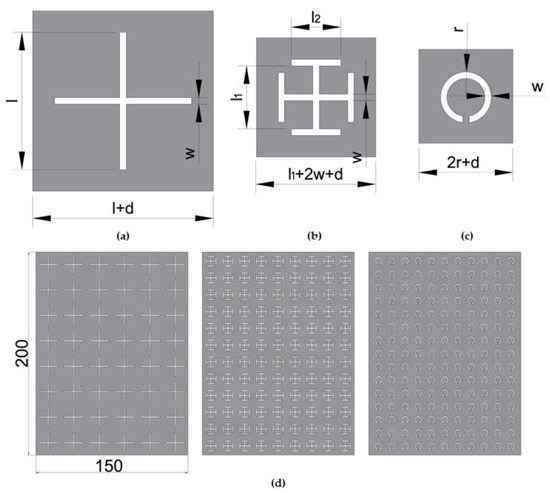
Figure 1.
Evaluated metasurface unit elements with the following geometric parameters: (a) complementary cross, (b) complementary Jerusalem cross, (c) complementary split-ring resonator, and (d) designed metasurfaces (dimensions in mm; the gray color is the copper cladding, the white color is the lack of copper cladding).
The proposed analysis can be interesting from the point of view of basic research (analysis of influence of various parameters on the behavior of metasurfaces—here, we are interested in a low sensitivity to any deformation of geometry), as well as from a point of view of applied research, where potential applications in wireless stress/deformation sensing are possible (in this case, we are interested in a high sensitivity to any deformation of geometry).
2. Materials and Methods
2.1. Metasurfaces Design
To compare the sensitivity of selected metasurface structures, they were each designed to work under the same operating conditions, which, in this case, means the following: to have a resonant behavior (in terms of s11 reflection coefficient) for a frequency of fr = 5 GHz. The first initial geometries were determined based on a numerical modeling-based optimization procedure. During the design process, the fixed value of the slot width, w = 0.9 mm, was assumed. This resulted in various sizes of the considered unit cells, as presented in Figure 1. The dimensions of the designed unit cells are shown in Table 1. All of the metasurfaces were manufactured using FR-4 laminates of thickness t = 1.5 mm, for which the dielectric properties were as follows: εr = 4.4 and tanδ = 0.02.

Table 1.
The dimensions of designed unit cells.
2.2. Simulation
The numerical models of the designed metasurface structures were developed and computed in the Comsol Multiphysics environment, based on the finite element method (FEM). The model geometry and description, as well as the computational mesh, are shown in Figure 2. The electromagnetic field excitation and detection were implemented through Port 1 and Port 2. The plane wavefront was generated by Port 1, and both ports received the scattered field (Port 1 for the s11 reflection coefficient and Port 2 for the s21 transmission coefficient determination). Because of the advances in electromagnetic field computing technology, in the case of the planned analyzes, there was no need to model the entire structure of the metasurface. In the proposed model, the Floquet-periodic boundary conditions were used in all of the external and parallel to z-direction boundary cases, to simulate an infinite 2D array of unit cell elements. This resulted in a significant reduction of computational mesh size, and thus a simplification of the numerical model. This assumption restricts the domain of the potential geometry deformations to the planar ones (in the x–y plane). Such a simplification of the model is acceptable, as it will be shown later in this paper, by comparison of the modeled and measured s11 reflection coefficient frequency responses. Perfectly matched layers (PMLs) are situated on the top and bottom of the computational domain in order to absorb the mode excited from the source port (Port 1), and any higher-order modes potentially generated by the periodic structure. The models were calculated in the frequency domain for 2–8 GHz frequency bands.
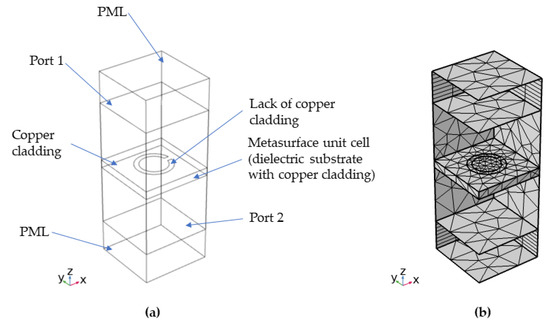
Figure 2.
Numerical model of a metasurface: (a) model geometry and description and (b) computational mesh shown on the selected model boundaries.
One of the analyzes carried out as part of the experiment concerned the impact of the surface deformation caused by the external mechanical forces. In this case, one of the side unit cell boundaries was fixed in x,y,z space, while the opposite one was loaded with an external force, as it is presented in Figure 3. First, the mechanical problem was solved and the deformed geometry was obtained. Next, the high-frequency electromagnetic problem was solved, based on the previously achieved deformed geometry. The equations solved during numerical the analysis are as follows [26]:
where E is the electric field, µr is the relative permeability, εr— is the relative permittivity, σ is the electric conductivity, k0 is the wave number, ω is the angular frequency, S is the stress, and Fv is the force per unit volume. The exemplary mesh used during numerical calculations consisted of 11,250 domain elements, 2662 boundary elements, and 380 edge elements.
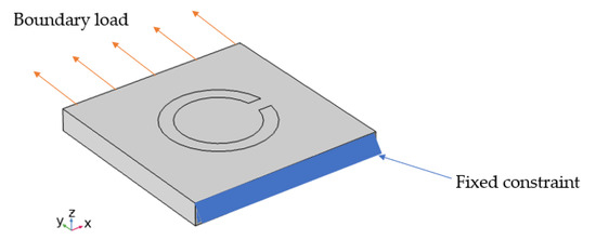
Figure 3.
External mechanical load application (in a y-direction).
2.3. Metasurface Fabrication
The metasurfaces were fabricated by etching the 1.5 mm thick FR-4 laminates with one side of 35 μm copper cladding. On the 200 mm × 150 mm laminates, the following matrixes of the unit elements were produced:
- 8 × 6 of cross-unit elements,
- 12 × 9 of Jerusalem cross-unit elements,
- 15 × 11 of split ring resonator unit elements.
The differences in the number of elements resulted from their size—a fixed value of the distance between the elements was adopted. The size of the metasurfaces was chosen in order to obtain an acceptable level of the reflected signal (the smaller the active size of the MS, the weaker the response).
2.4. Measuring System
In order to verify the correctness of the design process, measurements of the developed metasurfaces were taken. The measuring setup, as well as the fabricated metasurface structures and copper reference plate are presented in Figure 4. The examined structures were situated in an open, compact anechoic chamber equipped with pyramidal absorbers in order to reduce the side reflections and multiple reflections of the background of the object under test (OUT). A monostatic setup was utilized in order to obtain a complex s11 reflection coefficient. Measurements were made using a Schwarzbeck BBHA-9120D-718 double ridged broadband horn antenna, connected to the port of a Rohde&Schwarz (Munich, Germany) ZVB20 vector network analyzer (VNA). The power at the output of VNA’s port was set to 0 dBm (1 mW). The lift-off (antenna to OUT) distance was set to be 420 mm. First, the reference measurements without OUT and with a copper-plated plate of the same size as the metasurface structures were performed. Then, the measurements of the MS structures were made, and isolated responses of the metasurfaces were extracted by removing the influence of the interrogation antenna through the de-embedding procedure. A detailed description of this process can be found in the literature [20]. Finally, the total response of the metasurface was obtained by the subtraction de-embedded copper plate response of the MS response. Similar to the case of the simulations, measurements were performed in 2–8 GHz frequency bands.
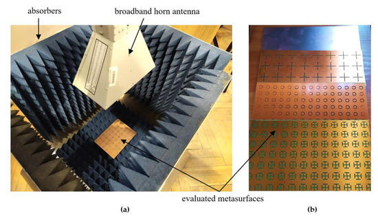
Figure 4.
Experimental setup for metasurfaces measurements: (a) photo of test stand and (b) photo of exemplary metasurfaces and reference conductive plate.
2.5. Description of the Experiment
The base metasurface structures developed for the proposed experiment are presented in Figure 1, and their dimensions are shown in Table 1. As was mentioned earlier, all of the structures (CR, JCR, and SRR) must operate under the same conditions. Thus, in the case of all of the base structures, for the reflection coefficient, there was resonance at a frequency of fr = 5 GHz. In order to determine the sensitivity of the analyzed metasurface structures to the changes of their geometric properties, an experiment was conducted in which the following deformations were carried out:
- slot width w change in the range of 0.3–1.5 mm,
- resonator to resonator distance d change in the range of 2–10 mm,
- dielectric laminate thickness t change in the range of 0.5–2.5 mm,
- mechanical deformation in the x-direction—constant strain up to 1% (external mechanical force F = 8.2764 kN in case of CR, F = 5.4615 kN in case of JCR, and F = 4.3098 kN in case of SRR),
- mechanical deformation in the y-direction—constant strain up to 1%.
The s11 reflection coefficient frequency response was determined for all of the above deformations. On its basis, the impact of a given deformation on the parameters of the resonance curve was examined, namely: the resonance frequency fr and the value of the reflection coefficient modulus in the resonance state |s11(fr)|. These parameters were used to assess the selected metasurfaces’ sensitivity to planar geometry distortions, because they can be treated as a measure of deviation from the assumed operating conditions (5 GHz resonance). This enabled us to obtain the distributions of fr and |s11(fr)| as a function of the degree of deformation. Such distributions were utilized for the final assessment in the next section.
3. Results and Discussion
The exemplary results of the simulations are presented in Figure 5. As was expected, the electric field was distributed only in the vicinity of the structural elements, where the copper layer was removed during the etching process. Based on the presented frequency responses of the scattering parameters, it is clearly visible that similar operating conditions were obtained in the case of all of the evaluated structures. The achieved resonant response was more selective in the case of the SRR.
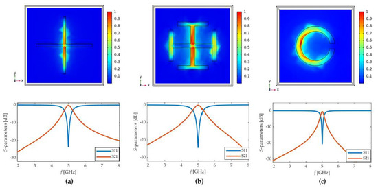
Figure 5.
Exemplary results of simulations—normalized electric field distribution (in case of resonant frequency) and frequency characteristics of scattering parameters s11 and s21 in the case of base structures (dimensions shown in Table 1): (a) cross cell geometry, (b) Jerusalem cross cell geometry, and (c) split ring resonator cell geometry.
The comparison of the resulting reflection coefficient |s11|obtained using numerical simulations and measurements is shown in Figure 6 for the selected MS structures. One can observe the good agreement. The resonant frequencies in both cases were very similar (the difference is less than 75 MHz), as well as the amplitudes in resonance (the difference of about 3 dB). The frequency responses obtained as a result of the calculations have standard, smooth shape characteristics for the resonance curves. In the case of the frequency responses obtained through the measurements, one can observe periodic oscillations caused by calibration errors during the de-embedding procedure. The agreement between the results of the simulations and measurements proves the correctness of the metasurface design procedure and numerical models. This means, the assumptions made during the modeling process, like the application of plane wavefront and Floquet-periodic boundary conditions, are valid and appropriate. Thus, the developed numerical models can be used for further analyses.
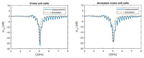
Figure 6.
Comparison of the simulated and measured frequency responses of the selected metasurfaces.
3.1. Study of Geometric Parameter Distortion
The results of the proposed numerical experiment are presented in Figure 7, Figure 8, Figure 9, Figure 10 and Figure 11. The distributions of the resonant frequency values, fr, for various slot widths, w; resonator to resonator distances, d; and for various dielectric laminate thicknesses, t, are shown in Figure 7, Figure 8 and Figure 9 for the CR, JCR, and SRR structures, respectively. The following general remarks can be drawn from the obtained distributions:
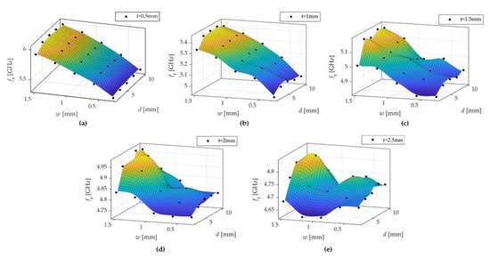
Figure 7.
Resonant frequency, fr, distribution as a function of slot width, w; resonator to resonator distance, d; and dielectric laminate thickness, t; in cases of cross (CR) cell geometry: (a) t = 0.5 mm, (b) t = 1.0 mm, (c) t = 1.5 mm, (d) t = 2.0 mm, (e) t = 2.5 mm.
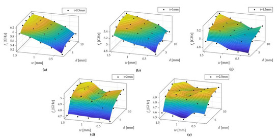
Figure 8.
Resonant frequency, fr, distribution as a function of the slot width, w; resonator to resonator distance, d; and dielectric laminate thickness, t, in cases of Jerusalem cross (JCR) cell geometry: (a) t = 0.5 mm, (b) t = 1.0 mm, (c) t = 1.5 mm, (d) t = 2.0 mm, and (e) t = 2.5 mm.
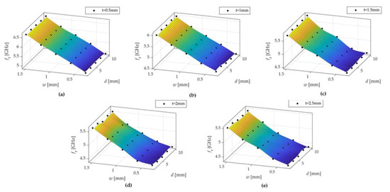
Figure 9.
Resonant frequency, fr, distribution as a function of slot width, w; resonator to resonator distance, d; and dielectric laminate thickness. t, in cases of split ring resonator (SRR) cell geometry: (a) t = 0.5 mm, (b) t = 1.0 mm, (c) t = 1.5 mm, (d) t = 2.0 mm, and (e) t = 2.5 mm.
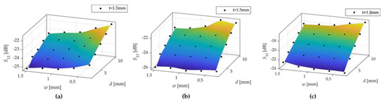
Figure 10.
Reflection coefficient modulus in the resonance state |s11(fr)| distribution as a function of slot width, w; and resonator to resonator distance, d, in cases of dielectric laminate thickness t = 1.5 mm: (a) cross cell geometry, (b) Jerusalem cross cell geometry, and (c) split-ring resonator cell geometry.
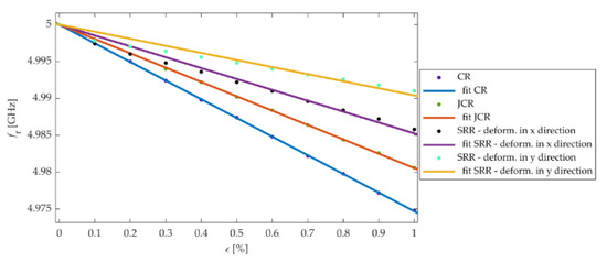
Figure 11.
Resonant frequency, fr, as a function of the strain caused by mechanical excitation (dielectric laminate thickness t = 1.5 mm).
- The resonant frequency, fr, increases with the increase of the slot width. In the case of the SRR structure, the relation is quasi-linear, contrary to other evaluated structures (CR and JCR), especially if the laminate thickness t is bigger than the optimal one.
- In the case of the SRR, the influence of the element to element distance d was negligible. For the CR structure, the fr slightly (for lower w values) and noticeably (for higher w values) increased with the increase of the d parameter. In the case of the JCR, independent of the w value, fr increased with the increase of distance d.
- Increase of the thickness of the dielectric substrate t (indirectly, an increase in frequency dependent equivalent permeability of substrate and capacitance in equivalent circuit [27,28,29]) causes a decrease of resonant frequency fr.
The quantitative description of the obtained results is presented in Table 2. Variations of the resonant frequency caused by the changes of the unit cell selected geometrical parameters are shown in the following two cases:
Table 2.
Resonance frequency variation under the influence of unit cells geometric parameters.
- whole parameters space is utilized (t Є ‹0.5–2.5› mm, w Є ‹0.3–1.5› mm, and d Є ‹2–10› mm);
- dielectric substrate thickness is restricted to t = 1.5 mm (w Є ‹0.3–1.5› mm and d Є ‹2–10› mm).
As one can observe, in both cases, the smallest variation caused by the changes of unit cells’ geometric parameters is for the CR structure, while the biggest is for the split-ring resonator. Thus, from the point of view of analyzed parameters changes, the CR structure seems to be the most stable and robust in terms of potential structure variations.
The next parameter that was evaluated was the amplitude of the frequency response for resonance |s11(fr)|. This parameter is not as reliable as the resonant frequency, because it is strongly dependent on, for example, metasurface fabrication quality. Despite this, the analysis was carried out, and its results were presented in Figure 10. One can observe similar distributions of |s11(fr)| in all of the evaluated structures. The resonant amplitude decreased (tends to 0) quasi-linearly with the increase of distance d. This effect can be easily explained—a lower spatial density of unit elements in the metasurface causes a lower power/amplitude response. For the CR and JCR structures, an increase in w causes a higher amplitude |s11(fr)|. A similar relation can be observed in the case of the SRR structure, only for lower values of d, this relation was inversed.
3.2. Study of Metasurface Mechanical Deformations
The next experiment concerned the mechanical excitation caused deformations. The results of this numerical analysis are shown in Figure 11. As was mentioned in the previous paragraph, metasurfaces were subjected to external stress in x- and y-directions, separately. The application of stress in an x-direction caused an extension of all of the geometric parameters in an x-direction, and a decrease in the y- and z-direction. Similarly, the application of stress in the y-direction (see Figure 3) caused an extension of all of the geometric parameters in a y-direction, and a decrease in the x- and z-directions. Influence of mechanical excitation on the behavior of the evaluated metasurfaces was also analyzed using fr and |s11(fr)| values. In the case of the CR and the JCR structures, because of their symmetry in orthogonal directions, these were the same results in the case of x- and y-direction stress application. In the case of the SRR cells-based material, there were various responses for various directions of mechanical excitation. Generally, in the case of all of the evaluated structures, there was a linear dependence between strain and resulting resonant frequency fr (operation in the linear range of stress–strain curve). The slope of the linear function depends on the metasurface structure. The highest sensitivity to mechanical excitation was for the CR structure, while the lowest sensitivity had the SRR stressed in the y-direction. The high sensitivity of the CR structure, in this case, may seem to contradict the result of the previous experiment (regarding the change of parameters w, d, and t), where the CR structure was stable and relatively a little dependent on the changes in geometry. However, it should be noted that (as already mentioned), in the case of stretching, the geometry changed in a completely different way than in the first experiment. When stretching the CR structure in an x-direction, there was an elongation (increase of l) and narrowing (decrease of w) of the cross arm parallel to the x-axis, and at the same time a shortening (decrease of l) and extension (increase of w) of the cross arm perpendicular to this axis. This operation was significantly different from, for example, increasing the width of both arms (changing the parameter w) from the previous experiment. This allowed us to state that the analysis of the metasurfaces’ susceptibility to geometry changes should be performed concerning specific applications and the resulting restrictions/parameters. Thanks to the consideration of the relative strain (in [%)), the influence of various dimensions of unit cells was minimized. Additionally (not shown in any Figure) the effect of the external mechanical excitation in the presented range had a negligible influence on the module of the reflection coefficient in the resonant state |s11(fr)|.
4. Conclusions
In this paper, the selected complementary metasurface structures (cross, Jerusalem cross, and split ring resonator) were evaluated, and their sensitivity to planar geometry deformations was analyzed. Each structure was designed to have similar operating conditions—to have a resonance behavior (fr = 5 GHz) in the case of the reflection coefficient. Numerical models of the considered metasurfaces were developed, and designed structures were fabricated. The measured responses of fabricated structures were in very good agreement with the numerical modeled ones.
During the proposed experiment, various deformations were applied to the previously designed structures. The main feature that was utilized for the evaluation was the resonant frequency fr. Another one (less reliable) was the amplitude of the reflection coefficient in the resonant state |s11(fr)|. Depending on the analysis type and the assumed criterion, various structures were optimal.
In the case of the geometric parameters (w, d, and t) of the distortion experiment, the best one (less sensitive to any changes) was cross unit cell-based metasurface, and the worse one was the split ring resonator structure.
If the external stress application experiment is considered (there is another mechanism for changing the geometrical parameters compared to the previous experiment, e.g., the slot expands in one direction, it narrows in the other), the cross structure is the most sensitive for such an influence. This means that, in the case of the current applications of metasurfaces, this structure should not be utilized in places where such planar deformations could happen. In the case of future applications (e.g., for the wireless measurement of 3D deformation), the CR structure would be applied.
The observed discrepancy of the results in both experiments (resulting from different mechanisms of changing the set of geometric parameters describing the structure of the metasurface) led us to the following conclusion: the analysis of the metasurfaces’ susceptibility to geometry changes should be performed concerning specific applications and the resulting restrictions/parameters.
In future work, more structures will be evaluated, as well as non-planar deformations’ influence on metasurface behavior will be investigated.
Author Contributions
P.L.—overall conception of the article, methodology, measurements, data analysis and writing the article; M.H.—metasurfaces design and numerical analysis. All authors have read and agreed to the published version of the manuscript.
Funding
This research was funded by the National Science Center, Poland (Narodowe Centrum Nauki, NCN), within the research project “Investigation of the impact of irregularities and deformations of the metasurface structure on their reflection properties for electromagnetic waves in the microwave and terahertz frequency band”, grant number 2018/02/X/ST7/02459. The APC was funded by the Research Fund of the Faculty of Electrical Engineering (West Pomeranian University of Technology, Szczecin, Poland).
Conflicts of Interest
The authors declare no conflict of interest.
References
- Oliveri, G.; Werner, D.H.; Massa, A. Reconfigurable electromagnetics through metamaterials—A review. Proc. IEEE 2015, 103, 1034–1056. [Google Scholar] [CrossRef]
- Withayachumnankul, W.; Abbott, D. Metamaterials in the Terahertz Regime. IEEE Photonics J. 2009, 1, 99–118. [Google Scholar] [CrossRef]
- Hsiao, H.H.; Chu, C.H.; Tsai, D.P. Fundamentals and Applications of Metasurfaces. Small Methods 2017, 1, 1600064. [Google Scholar] [CrossRef]
- Achouri, K.; Caloz, C. Design, concepts, and applications of electromagnetic metasurfaces. Nanophotonics 2018, 7, 1095–1116. [Google Scholar] [CrossRef]
- Alù, A.; Engheta, N. Pairing an Epsilon-Negative Slab with a Mu-Negative Slab: Resonance, Tunneling and Transparency. IEEE Trans. Antennas Propag. 2003, 51, 2558–2571. [Google Scholar] [CrossRef]
- Tretyakov, S.A. Metasurfaces for general transformations of electromagnetic fields. Philos. Trans. R. Soc. A 2015, 373, 20140362. [Google Scholar] [CrossRef] [PubMed]
- Saleh, A.A.; Abdullah, A.S. High Gain Circular Patch Antenna Using Metamaterial Supperstrate for DSRS System Applications. J. Telecommun. 2014, 27, 1–6. [Google Scholar]
- McVay, J.; Hoorfar, A.; Engheta, N. Peano high-impedance surfaces. Radio Sci. 2005, 40, RS6S03. [Google Scholar] [CrossRef]
- Ebrahimi, A.; Withayachumnankul, W.; Al-Sarawi, S.; Abbott, D. High-sensitivity metamaterial-inspired sensor for microfluidic dielectric characterization. IEEE Sens. J. 2014, 14, 1345–1351. [Google Scholar] [CrossRef]
- Saghati, A.P.; Batra, J.S.; Kameoka, J.; Entesari, K. A metamaterial-inspired wideband microwave interferometry sensor for dielectric spectroscopy of liquid chemicals. IEEE Trans. Microw. Theory Tech. 2017, 65, 2558–2571. [Google Scholar] [CrossRef]
- Kim, Y.J.; Hwang, J.S.; Khuyen, B.X.; Tung, B.S.; Kim, K.W.; Rhee, J.Y.; Chen, L.Y.; Lee, Y.P. Flexible ultrathin metamaterial absorber for wide frequency band, based on conductive fibers. Sci. Technol. Adv. Mater. 2018, 19, 711–717. [Google Scholar] [CrossRef]
- Zhang, Y.; Zhao, J.; Cao, J.; Mao, B. Microwave Metamaterial Absorber for Non-Destructive Sensing Applications of Grain. Sensors 2018, 18, 1912. [Google Scholar] [CrossRef] [PubMed]
- Radi, Y.; Simovski, C.R.; Tretyakov, S.A. Thin perfect absorbers for electromagnetic waves: Theory, design, and realizations. Phys. Rev. Appl. 2015, 3, 037001. [Google Scholar] [CrossRef]
- Badloe, T.; Mun, J.; Rho, J. Metasurfaces-Based Absorption and Reflection Control: Perfect Absorbers and Reflectors. J. Nanomater. 2017, 2017. [Google Scholar] [CrossRef]
- Zhao, Y.; Qing, A.; Meng, Y.; Song, Z.; Lin, C. Dual-band Circular Polarizer Based on Simultaneous Anisotropy and Chirality in Planar Metamaterial. Sci. Rep. 2018, 8, 1729. [Google Scholar] [CrossRef]
- Sauviac, B.; Simovski, C.R.; Tretyakov, S.A. Double Split-Ring Resonators: Analytical Modeling and Numerical Simulations. Electromagnetics 2004, 24, 317–338. [Google Scholar] [CrossRef]
- Savin, A.; Steigmann, R.; Bruma, A.; Sturm, R. An Electromagnetic Sensor with a Metamaterial Lens for Nondestructive Evaluation of Composite Materials. Sensors 2015, 15, 15903–15920. [Google Scholar] [CrossRef]
- Khorasaninejad, M.; Chen, W.T.; Devlin, R.C.; Oh, J.; Zhu, A.Y.; Capasso, F. Metalenses at visible wavelengths: Diffraction-limited focusing and subwavelength resolution imaging. Science 2016, 352, 1190–1194. [Google Scholar] [CrossRef]
- Chen, K.; Feng, Y.; Monticone, F.; Zhao, J.; Zhu, B.; Jiang, T.; Zhang, L.; Kim, Y.; Ding, X.; Zhang, S.; et al. A reconfigurable active Huygens’ metalens. Adv. Mater. 2017, 29, 1606422. [Google Scholar] [CrossRef]
- Gargari, A.M.; Zarifi, M.H.; Markley, L. Passive Matched Mushroom Structure for a High Sensitivity Low Profile Antenna-Based Material Detection System. IEEE Sens. J. 2019, 19, 6154–6162. [Google Scholar] [CrossRef]
- Ramya, S.; Srinivasa Rao, I. An Ultra-Thin Compact Wideband Metamaterial Absorber. Radioengineering 2018, 27, 364–372. [Google Scholar] [CrossRef]
- Ahamed, E.; Hasan, M.M.; Faruque, M.R.I.; Mansor, M.F.B.; Abdullah, S.; Islam, M.T. Left-handed metamaterial inspired by joint T-D geometry on flexible NiAl2O4 substrate. PLoS ONE 2018, 13, e0199150. [Google Scholar] [CrossRef] [PubMed]
- Butrylo, B.; Steckiewicz, A. Characterization of properties and magnetic field distribution in conductive thin-film laminar materials. In Proceedings of the Conference on Fundamentals of Electrotechnics and Circuits Theory, Gliwice Ustron, Poland, 16–19 May 2018. [Google Scholar]
- Wang, J.; Qu, S.; Xu, Z.; Ma, H.; Yang, Y.; Gu, C. A Controllable Magnetic Metamaterial: Split-Ring Resonator with Rotated Inner Ring. IEEE Trans. Antennas Propag. 2008, 56, 2018–2022. [Google Scholar] [CrossRef]
- Gomon, D.; Sedykh, E.; Rodríguez, S.; Idelfonso, T.M.; Zaitsev, K.; Vozianova, A.; Khodzitsky, M.A. Influence of the geometric parameters of the electrical ring resonator metasurface on the performance of metamaterial absorbers for terahertz applications. Chin. Optics 2018, 11, 47–59. [Google Scholar]
- Herbko, M.; Lopato, P. Double patch sensor for identification of stress level and direction. Int. J. RF Microw. Comput. Aided Eng. 2019, 29. [Google Scholar] [CrossRef]
- Duran-Sindreu, M.; Naqui, J.; Paredes, F.; Bonache, J.; Martin, F. Electrically Small Resonators for Planar Metamaterial, Microwave Circuit and Antenna Design: A Comparative Analysis. Appl. Sci. 2012, 2, 375–395. [Google Scholar] [CrossRef]
- Marques, R.; Martin, F.; Sorolla, M. Metamaterials with Negative Parameters—Theory, Design and Microwave Applications; John Wiley Sons: Hoboken, NJ, USA, 2008. [Google Scholar]
- Marwaha, A. An Accurate Approach of Mathematical Modelling of SRR and SR for Metamaterials. J. Eng. Sci. Technol. Rev. 2016, 9, 82–86. [Google Scholar]
© 2019 by the authors. Licensee MDPI, Basel, Switzerland. This article is an open access article distributed under the terms and conditions of the Creative Commons Attribution (CC BY) license (http://creativecommons.org/licenses/by/4.0/).