Article

The Influence of Laser Sintering Modes on the Conductivity and Microstructure of Silver Nanoparticle Arrays Formed by Dry Aerosol Printing

1
Department of Physical and Quantum Electronics, Moscow Institute of Physics and Technology (National Research University), Dolgoprudny 141701, Russia
2
JSC ESTO Co., Zelenograd 124460, Russia
*
Author to whom correspondence should be addressed.
Appl. Sci. 2020, 10(1), 246; https://doi.org/10.3390/app10010246
Submission received: 10 November 2019 / Revised: 10 December 2019 / Accepted: 25 December 2019 / Published: 28 December 2019
(This article belongs to the Section Nanotechnology and Applied Nanosciences)

Abstract

:
The demand for the development of local laser sintering of nanoparticle arrays is explained by the expanding needs for printed electronics for functional microstructure formation, on heat-sensitive substrates in particular. This work is based on the research into the sintering of arrays of silver nanoparticles synthesized in a spark discharge and deposited on a substrate by focused aerosol flow. The sintering was done by continuous and pulsed lasers with wavelengths 527, 980 and 1054 nm. Sintered samples were studied by measuring the resistivity, cross-section profile area and microstructure features. The highest average conductivity, equal to the half of the bulk silver conductivity, was achieved when sintering by continuous radiation with a wavelength 980 nm. The results showed that when using pulsed radiation the direct heating of nanoparticles in the sample surface layer dominates with the formation of a pore-free conductive layer of around 0.5 μm thick and crystallite of 70–80 nm size. It was found that laser sintering by radiation with a wavelength 527 nm required an order of magnitude lower specific energy costs as compared to the longwave laser radiation. The high energy efficiency of laser sintering is explained by special conditions for radiation absorption at plasmon resonance.

1. Introduction

When forming electronic elements by printing with nanoparticles (NP), an important process that ensures the electronic properties of these elements is the sintering of NP arrays deposited on the substrate. In recent years, studies and applications of local laser sintering of NP arrays on substrates have been developing, which significantly expands the possibilities of micron-size printing methods in the areas of heat-sensitive plastic substrates and a variety of NP materials used [1,2]. In particular, the method of laser sintering of micron-size conductors from silver NPs and organic thin-film transistors on polyethylene naphthalate (PEN) substrates was studied in [3,4]. Most metals used for the synthesis of NPs, e.g., copper or aluminum, have a high oxidation reactivity in ambient conditions. It results in the formation of oxide insulating film 1–3 nm thick on a surface, preventing the high conductivity between particles. To minimize the oxygen flow to the surface of NPs a layer of noble metal or other inert coating substance (thiol, polymer) may be applied [5,6]. Also, to prevent oxidation processes, it is possible to form samples in a high vacuum or in an inert gas environment [7].
The use of laser sintering for micron-size elements formed by the developing aerosol printing technology, which is based on selective deposition of aerodynamically focused NP streams onto the substrate is promising. In the first implementation of the technology samples were being formed by microdrops from the dispersion of NPs (inks) [8]. Aerosol printing allows to form functional elements on the substrates with a minimum line width of around 10 μm, which is much lower than while using inkjet and screen printing technologies [9]. However, when NPs are delivered to the substrate as a part of the ink, solvent and other organic additives must be removed before sintering. This makes the sintering process of NP array dependent on the composition of the ink used.
In the last decade, many studies have been done in the field of conductive lines formation by selective laser sintering of NP arrays formed by ink printing, mainly on heat-sensitive substrates (PET, PEN, polyamide), e.g., [10,11,12,13]. Sintering processes were studied using continuous (CW) and pulsed nanosecond and picosecond laser sources operating at 248, 532 and 1064 nm. The processes of laser radiation absorption by silver NPs and energy transfer to the substrate were studied experimentally and by computer simulation. The high specific conductivity of sintered silver NP arrays, 4–6 times smaller than for bulk silver, was demonstrated in studies using inks of silver NPs of less than 50 nm in size and a mass fraction of 34–75 wt% and with the use of nanosecond pulsed laser sources with a wavelength 532 nm [10,12].
Special attention was paid to the process of removing solvents and other additives from the ink deposited on the substrate, as this procedure improves the laser sintering efficiency of the silver NP arrays. In recent articles the time spent on drying of deposited inks at 60–80 °C has been reduced from 24 hours to 30–60 min. The use of ink with a high mass fraction of silver NPs (70–75 wt%) was a fundamentally new step in this direction. It allowed to evaporate the solvent and the volatile additives from the ink at room temperature, by leaving the ink to dry for 1 h [12]. However, the problem of drying the ink deposited on the substrate remains.
Recently [14,15,16] a new approach in aerosol printing has been proposed with no ink used. In this approach, NPs just before being used are synthesized in the processes of a spark discharge in a flowing gas between electrodes of the material desired [17]. The aerosol stream of NPs is focused and delivered to the treated surface, the particles are deposited in a dry form without a solvent. Recent studies have shown a high efficiency and productivity of dry aerosol printing in comparison with the other additive technologies [15,18,19,20]. Electrode materials used as sources of NPs in the process of dry aerosol printing are not limited by storage conditions and expiry date. Synthesized in an inert gas stream aerosol NPs are characterized by a high purity of the material, which allows to form structures free from impurities and surfactants [21]. This allows one to sinter NP arrays with laser radiation immediately after their deposition, which is of interest for mass production of microelectronic and photonic elements, including manufacturing on curved and heat-sensitive substrates [10,22,23].
In this regard, an urgent scientific interest arises to study the efficiency of laser radiation absorption by a NP array. It is well-known that the absorption ability of NPs depends both on the wavelength of incident laser radiation and their shape and size due to plasmon effects [24,25]. It is expected that in the process of the powder structure monolithization caused by laser sintering, its optical absorption coefficient decreases due to consolidation and enlargement of the particles comprising the structure, whereas the reflection coefficient increases. The efficiency of laser energy absorption consequently drops. Thus, the process of laser radiation absorption during the sintering of NP arrays appears to be essentially nonlinear and requires experimental research to be done.
During the study of laser sintering of metal NP arrays, it is convenient to characterize the efficiency of the process by specific electrical values—conductivity and/or resistance, in comparison with bulk material [11,22,26]. In this paper, the influence of laser radiation energy parameters in sintering processes on the electrical conductivity and microstructure of silver NP arrays is investigated. It is silver that is attractive for the purposes of conductive microstructure formation due to the high parameter values of electrical conductivity and plasticity and low melting point, which essentially decreases for NPs together with their size diminishing. Sintering processes were done for continuous and pulsed laser sources with wavelengths 527, 980 and 1054 nm. Conductivity and morphology of microstructures were studied for the samples obtained.

2. Materials and Methods

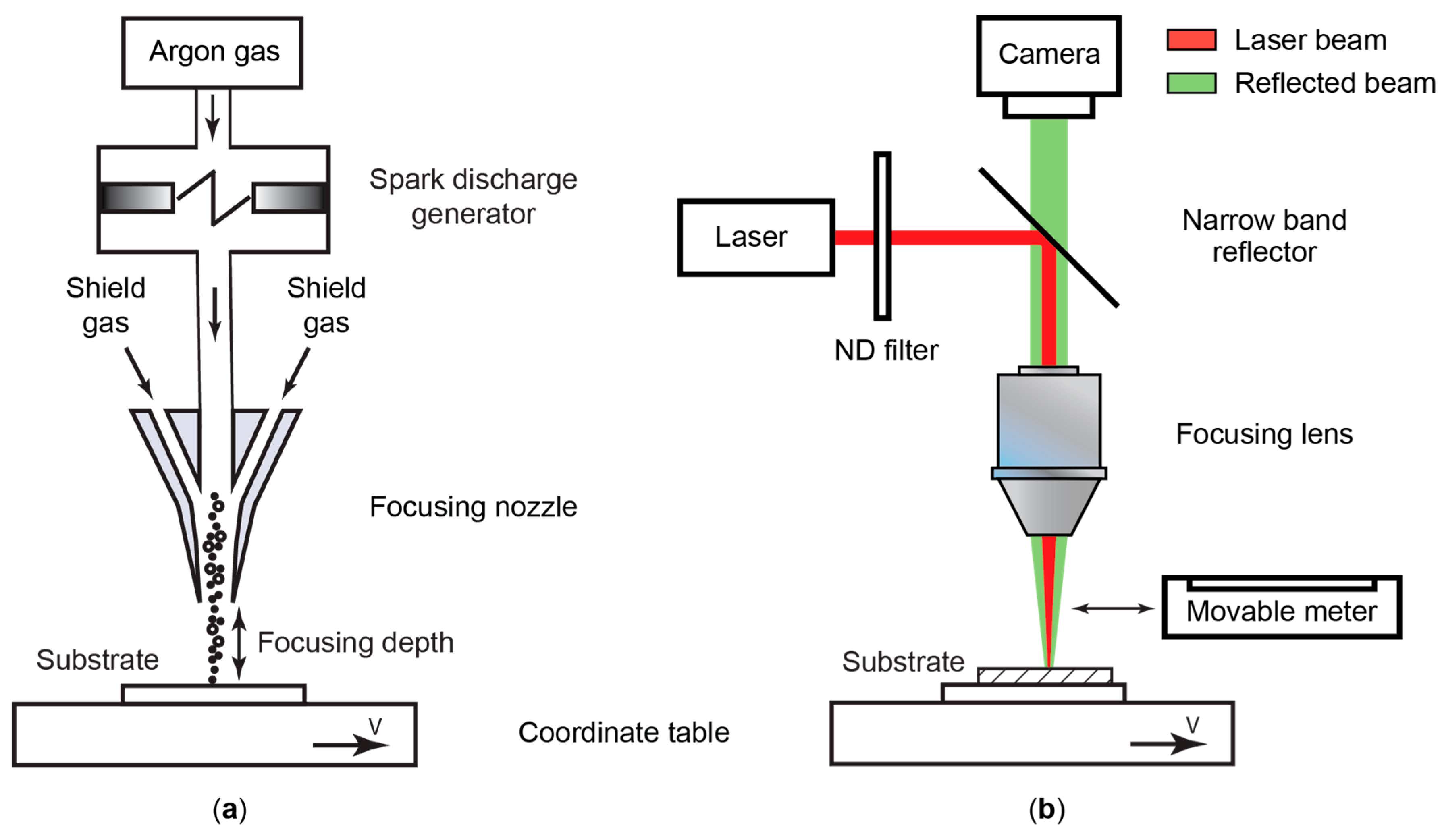
This research is aimed to investigate the laser sintering processes of silver NP arrays synthesized by electrical erosion in a spark discharge between silver electrodes in an argon flow atmosphere and deposited on a substrate. The setup for the micron-sized elements formation from such NPs is schematically presented in Figure 1a. NPs with an average size of around 10 nm were synthesized in a spark discharge chamber. Further an aerosol of those particles with the high-purity argon flow entered the focusing aerodynamic system in the form of the nozzle, described earlier in [14,27]. The design of the nozzle provides an additional external compressing gas stream, which allows to control the cross-section of the aerosol stream by adjusting its parameters [28,
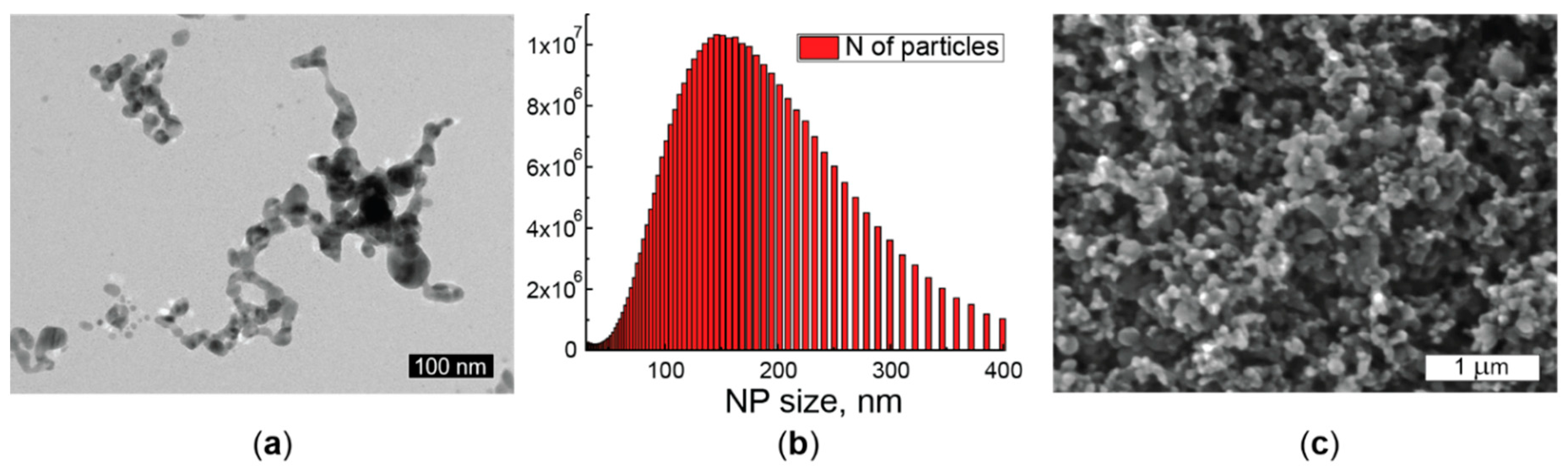
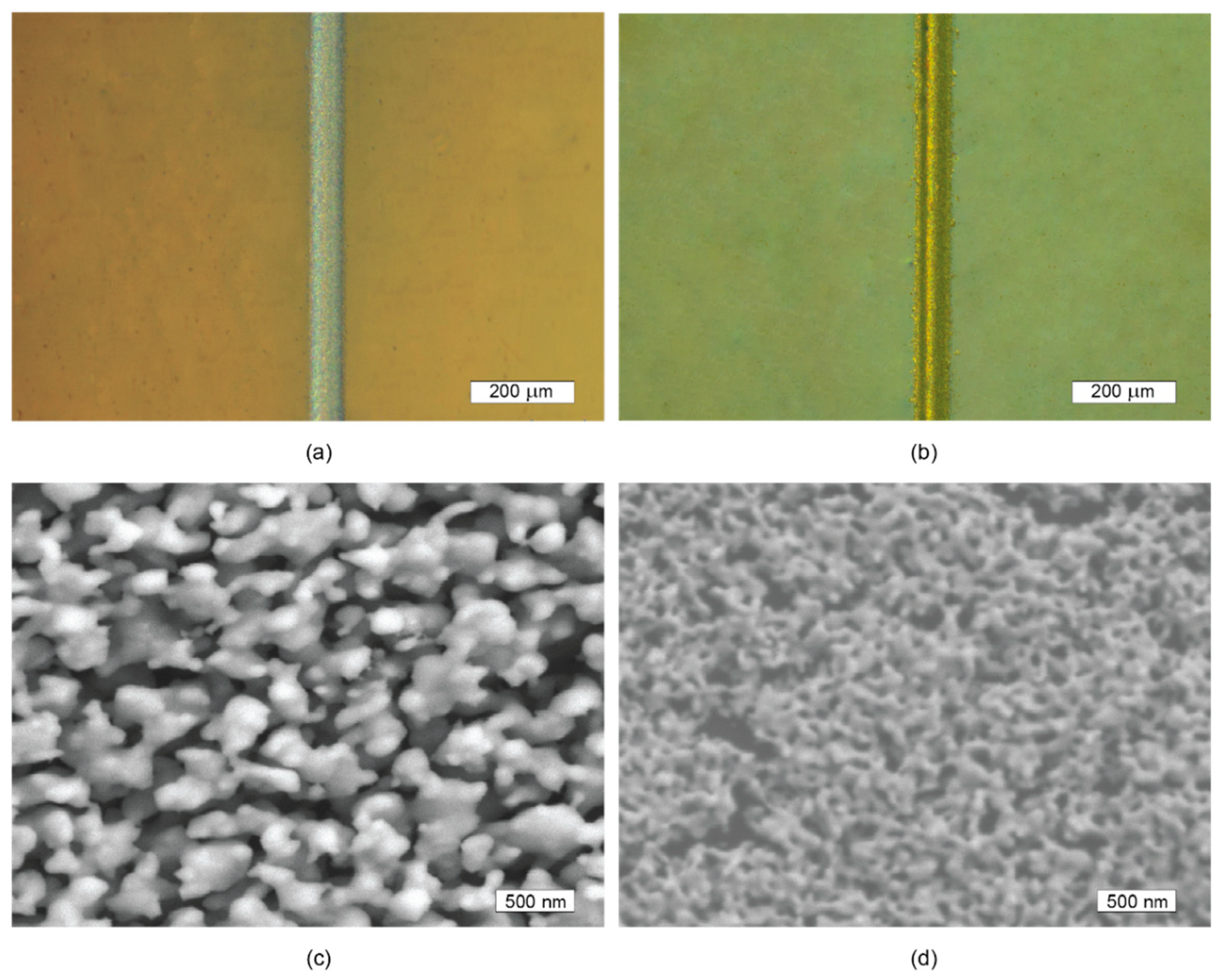
29]. In addition, the experimental setup enables to control the distance between the nozzle and the substrate within its change up to 4 mm, which makes printing on a curved surface possible. Silver NP arrays in the form of lines were deposited on polished silicon substrates 540 μm thick placed on a precision movable coordinate table. To demonstrate the applicability of the proposed approach for the formation of silver NP arrays on heat-sensitive substrates, we conducted similar experiments on the deposition of silver NP arrays by dry aerosol printing and their subsequent sintering by pulsed laser radiation on the polyamide substrates 140 μm thick. These lines had cross-sections in the form of a Gaussian distribution with the FWHM parameter in the range of 40–80 μm and a height parameter of 10–20 μm (Figure 2b). The lines were formed between two prefabricated silver contact pads about 5 μm thick spaced 5 mm apart (Figure 2a).
Contact pads were used to measure the conductivity of the sintered lines by a two-contact method. They were formed by an AMT AJ 15XE aerosol printer (Neotech, Nuremberg, Germany) by depositing microdrops of silver NP ink and then sintered in a conventional resistive furnace at 250 °C for 20 min. The ink used for printing was a mixture of PG-007 MOP и PG007-EG (PARU Co., Ltd., Sunchon, Republic of Korea) in a volume ratio of 3:1, with a mass concentration and an average nanoparticle size 46% and 18 nm, respectively. The method described provides a high conductivity of the material for the contact pads, equal to the half of the specific conductivity for bulk silver [30]. This peculiarity is important for voltage drop minimization on contact pads while measuring the conductivity of the studied lines.
The sintering process of the resulting silver NP arrays in the form of lines was done under the influence of a laser radiation with wavelengths 527, 980 and 1054 nm. The characteristics of the lasers used are given in Table 1. Four types of CW and pulsed laser sources were installed alternately on the laser position into optical stand being combined with the aerosol printing setup. The optical setup is schematically presented in Figure 1b. The use of the same coordinate table in the time-spaced processes of printing and subsequent sintering made it possible to continuously form and sinter NP lines. Sintering processes under the influence of laser radiation were controlled by adjusting the power and diameter of the laser beam, and the speed of movement both of the substrate and the sample. Pulsed laser sources were additionally characterized by a pulse repetition rate, chosen equal to 4 kHz for the research, and a pulse duration equal to 20 ns. Measurements for laser radiation parameters were taken by the following devices: BeamOn HR (Duma Optronics, Nesher, Israel) for measurements of the laser beam diameter in the plane of the sample, F150A-BB-26 (Ophir, North Logan, UT, USA) for measurements of the radiation power incident on the sample and 0D-08A (Avesta, Ltd., Troitsk, Russia) with an oscilloscope for pulse repetition rate measurements.
To obtain data on the average electrical conductivity σ over cross-section of the sintered silver lines, the absolute resistance of the lines, their cross-section profile and length were measured by a 287 multimeter (Fluke, Everett, WA, USA) DCM 3D optical profiler (Leica, Wetzlar, Germany) and VHX-1000 optical microscope (Keyence, Itasca, IL, USA) respectively.
The shapes and sizes of the deposited NP and their agglomerates were studied by transmission electron microscope (TEM) JEM-2100 (JEOL, Ltd., Tokyo, Japan). Additionally, the statistical size distribution of silver NP agglomerates in the aerosol stream after the focusing nozzle was measured by the aerosol NP analyzer SMPS 3936 (TSI Inc., Shoreview, MN, USA).
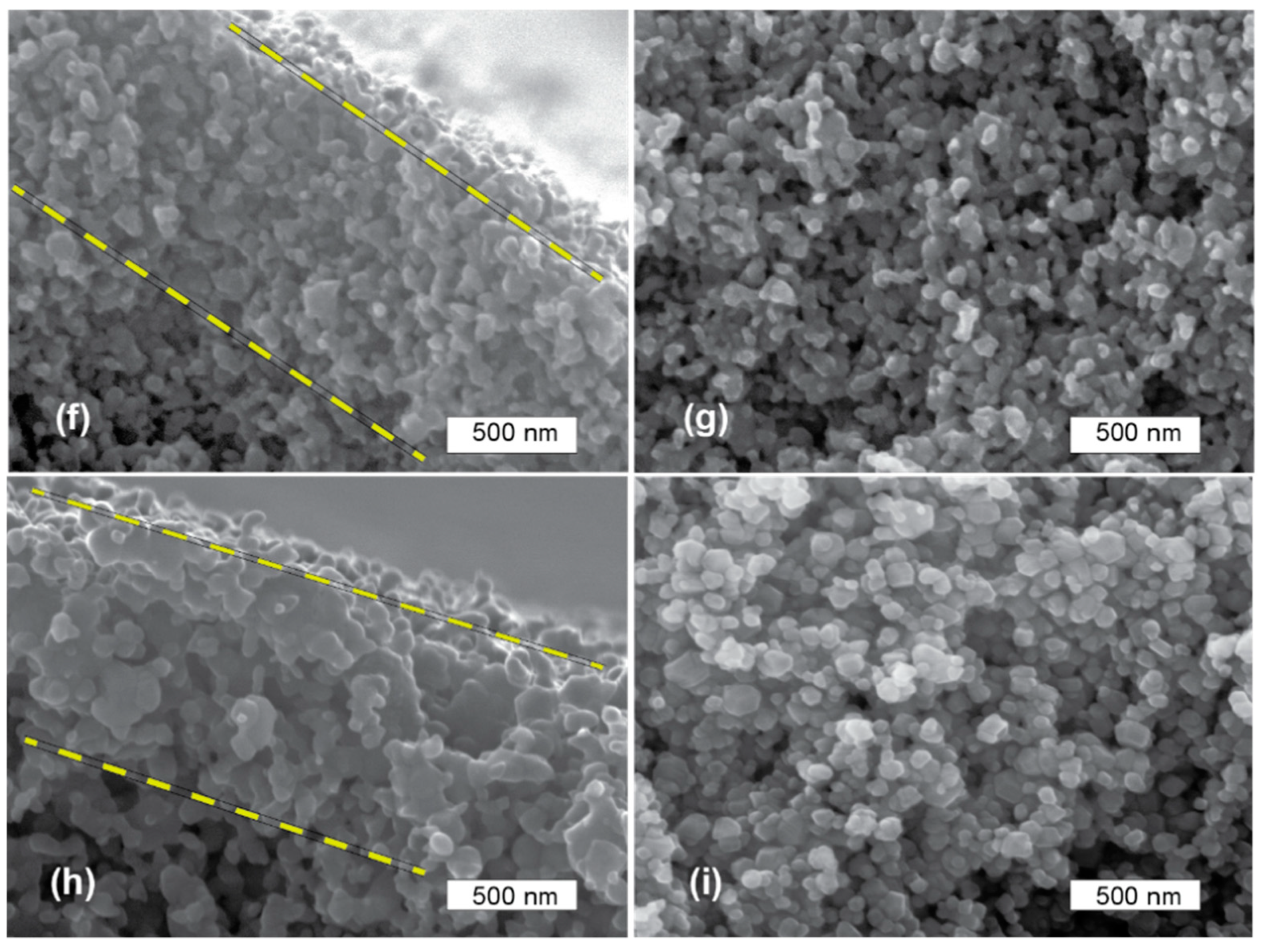
To study the microstructure of sintered samples in the form of lines along the cross-section, their fractures were prepared. To obtain a brittle fracture and minimize the effects of silver crystallites plastic deformation, the samples were cooled in liquid nitrogen, after which a transverse brittle fracture of the line was made together with the substrate. The transverse line fractures obtained in this way were studied by scanning electron microscope (SEM) JSM 7001F (JEOL, Ltd., Tokyo, Japan). The porosity pattern and its boundaries were determined from the images of fractures, the average crystallites statistical sizes were estimated for processing of over 400 particles, approximating them with a sphere. Crystallite sizes were compared for a pore-free layer near the array outer surface and for a porous microstructure in the central part of the line fracture. The samples surface roughness was studied by atomic force microscopy (AFM) using a Solver PRO-M system (NT-MDT, Zelenograd, Russia).

3. Results

3.1. Characterization of Silver Nanoparticle Printed Arrays

During the aerosol flow movement from the spark discharge generator to the substrate, primary silver NPs with an average size of around 10 nm experience many collisions and this results in their combination into dendrite-like agglomerates. In the process of aerosol printing NP arrays are formed by the deposition of such agglomerates on the substrate. A characteristic image of agglomerates composed of primary silver NPs obtained by TEM is presented in Figure 3a. It should be noted that the size range of agglomerates measured from TEM images of 100–300 nm correlates well with the agglomerates average size of 160 nm, determined from the size distribution of the agglomerate concentration measured in the aerosol flow by NP analyzer SMPS 3936 (Figure 3b). The line-shaped array printed on a substrate by the above mentioned NP agglomerates is characterized by high submicron porosity and a small number of point contacts between NPs. The SEM image of the NP array microstructure as shown in Figure 3c evidently proves this. The statistical analysis of a large number of NPs (more than 400) obtained by SEM images of arrays gave the average size of 15 nm. Printed arrays of silver NPs are characterized by low specific conductivity of around 103 (Ohm·m)−1.

3.2. Electrical Conductivity of Laser Sintered NP Arrays

Laser sintering of silver NP arrays in the form of lines was done by each of the four lasers with a large number of regimes. They were characterized by a change of supplied specific energy per surface unit in the range from five to six magnitude orders. At a given laser radiation average power, the specific energy supplied to the surface of the array was controlled by changing the speed of the laser beam relative to the line. In all the experiments, the diameter of the laser beam exceeded the width of the line. It provided the radiation energy supply to the entire surface of the sample during the movement of the beam. Figure 4a–d shows the experimental dependencies of the average specific conductivity σ of sintered silver NP arrays at several fixed values of the average laser power versus the specific energy e in logarithmic coordinates. Here, each experimental point on the graphs σ(e) corresponds to the average value of the conductivity measurements of at least three samples.
The σ(e) behavior tends to increase in conductivity maximum value with an increase of radiation power for all laser radiation types. There are exceptions to this behavior shown in Figure 4a–c, where for the maximum laser powers the dependences σ(e) are lower than for the preceding powers. This may indicate the existence of some optimal radiation power resulting in maximum conductivity for a particular type of radiation. Most of the obtained dependences σ(e) are characterized by monotonically increasing curves. However, only for pulsed lasers (Figure 4a,b) the dependences of the average conductivity on the specific energy have a pronounced maximum. It is worth mentioning that with the energy density increase for radiation with a wavelength 1054 nm (Figure 4b) the decay in conductivity tends to go smoothly, while for radiation with a wavelength 527 nm (Figure 4a) the conductivity decreases steeply, reaching lower values as compared to the minimum power. It can be assumed that there is an optimum for the energy density supplied to the sample in pulse mode, in which higher energy values lead to degrading or destruction of the sample. In terms of the absolute value of specific conductivity, the highest values were achieved for sintered samples using CW laser radiation with a wavelength 980 nm. The specific conductivity achieved in this regime corresponds to the half of the bulk silver conductivity (Figure 4d).
It should be noted that CW laser sintering showed a higher specific conductivity in comparison with the pulsed laser sintering. The sintering of samples under the laser radiation with a wavelength 527 nm required significantly lower specific energy costs as compared to the longwave laser sintering. Similarly, it is more efficient to conduct sintering with pulsed laser radiation than with CW.

3.3. Microstructure of Laser Sintered NP Arrays

Due to the fact that the laser radiation energy enters the NP array through the surface, the sintered sample microstructure is expected to be inhomogeneous in depth. Therefore, to clarify the mechanisms of the laser sintering process, we studied the internal microstructure of sintered silver NP arrays in the form of lines for their transverse fractures by SEM. Figure 5a–i shows typical SEM images for transverse line fractures sintered by laser radiation in optimal regimes for each type of laser corresponding to the highest average line conductivities.
The SEM image in Figure 5a shows a general view of a sintered line characteristic fracture over the substrate for an optimal sintering regime corresponding to 980 nm wavelength. Figure 5b–i shows SEM images for the external fracture area, including the border of the sample surface, and the internal fracture area, obtained with a larger magnification in the areas marked with the red frames in the characteristic image of the line fracture general view (Figure 5a). The image analysis of sintered line fractures allows to see a common mechanism for the four types of laser radiation. The external surface of the sample fractures contains almost a non-porous zone of densely sintered material. In the images this zone is highlighted between two yellow dotted lines (Figure 5b,d,f,h). Deeper in the array after the pore-free zone there follows a transition zone with separate submicron pores. Further to the fracture middle part there is a microstructure with an approximate uniform submicron porosity (Figure 5c,e,g,i). The thickness of the non-porous layer, achieved from SEM images of sample fractures for the four types of laser radiation used, is presented in Table 2.
It should be noted that the sintered pore-free layer thickness range for all types of lasers is 0.5–1 μm. This layer differs from the rest of the fracture microstructure by the absence of submicron pores and by the large crystallite average sizes compared to the porous zone in the depth of the samples. The measurement results are given in Table 2. Crystallite sizes measurements in the zones discussed were done using fractures SEM images with crystallites approximated by an equivalent circle with an equal area. The average crystallite size was attained by averaging the sizes of many individual crystallites in amount of over 400.
Comparing the parameters of microstructures sintered by different types of laser radiation (Table 2), we note that the thickness of the sintered pore-free layer as well as the average crystallite sizes increase during the transition from pulsed laser sintering to CW sintering. The thickness also grows with an increase in the wavelength of pulsed laser radiation. In this case, the average crystallite sizes grow with an increase in the wavelength of both pulsed and CW laser radiation. Within each sample, the average crystallite sizes in the non-porous layer are much larger than for crystallites in the porous zone.
It should be pointed out that the surface of the samples under the study is characterized by a low RMS roughness in the range of 40–70 nm, same for sintered and untreated samples, measured by AFM in the area 10 × 10 μm2.
The use of polished silicon substrates in the experiments made it possible to study the fractures microstructure of sintered lines by SEM. As the method proposed for forming lines from silver NPs is promising for heat-sensitive substrates, we conducted preliminary experiments for laser sintering of silver NP arrays on polyamide substrates. Silver NP lines deposited on polyamide substrates were sintered by pulsed laser radiation with wavelengths 527 and 1054 nm with sintering process parameters close to the optimal regimes defined for lines sintered on silicon substrates. The averaged specific conductivity for four lines sintered by laser radiation with wavelength 527 and 1054 nm are presented in Table 3. It is shown that the average specific conductivity of silver lines was reached three times higher on polyamide substrates than on silicon substrates.
Considering the size of laser beam exceeded the linewidth of the printed silver lines, it was important to conduct the experiments on the laser radiation interaction with the substrate at the line edges.
Figure 6a,b shows that the applied laser sintering regimes left the surface of the polyamide substrate near the line edges intact. The microstructure of the surface of lines sintered on polyamide substrates was investigated by SEM. Figure 6c,d shows the surface layer from sintered NP with well-formed bonds between them and the absence of large micron pores.

4. Discussion

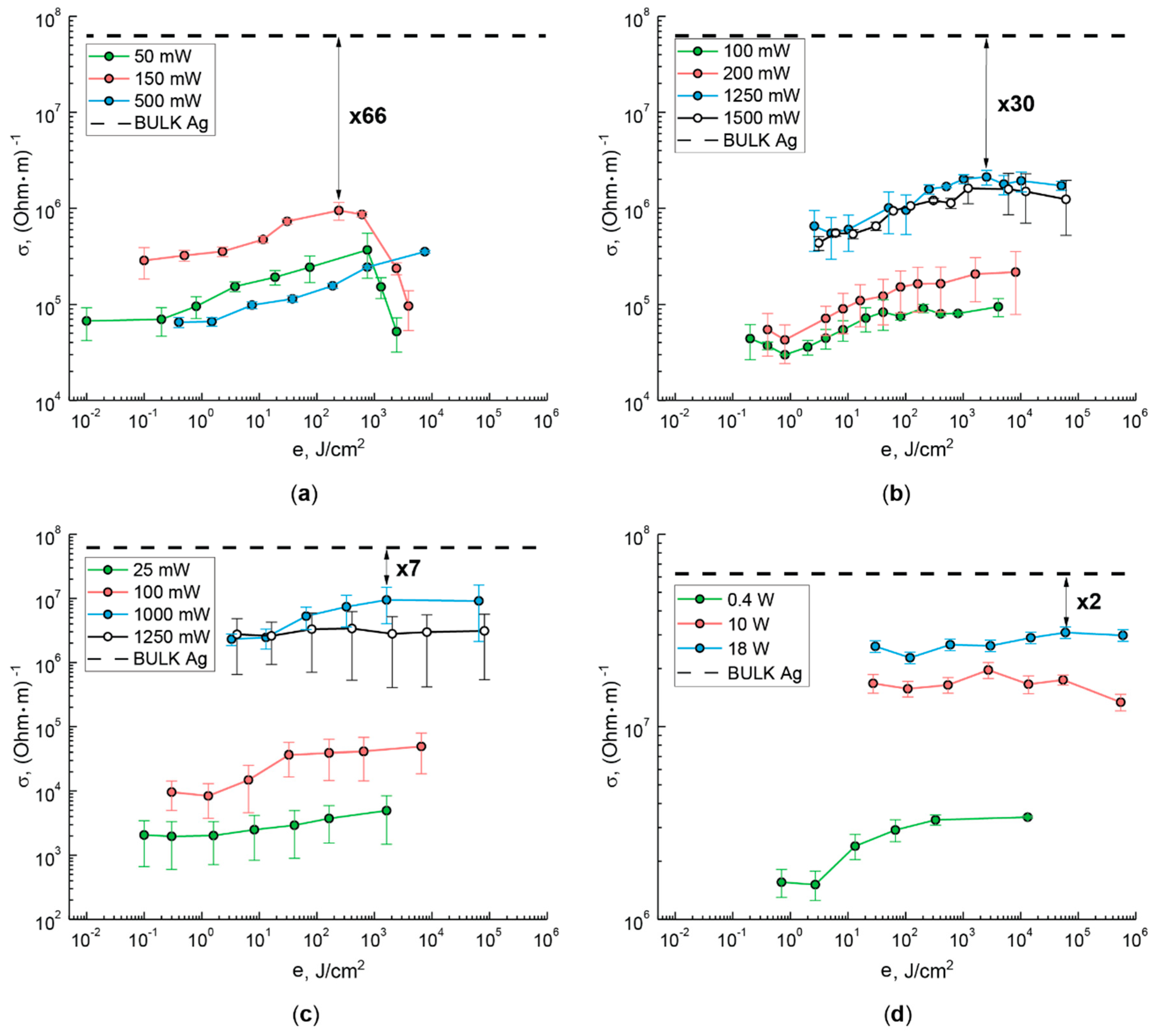
Comparing the data on average specific conductivity σ(e) (Figure 4) and on microstructure (Figure 5, Table 2) of silver NP arrays sintered by four types of laser radiation, we assume that the best conductivity areas in all cases are non-porous external layers with thickness in the range 0.5–1 μm. The formed contacts between crystallites and their large size values indicate the better conductivity of pore-free external layers in comparison with porous zones. In contrast, in porous zones, silver crystallites are connected in agglomerates with conductive contacts inside, between which there are many submicron pores, potentially reducing conductivity. Particularly this occurs in porous zones of samples sintered by pulsed laser radiation (Figure 5c,e). Assuming that the specific conductivities in the porous and pore-free zones of the sample are significantly different and homogeneous, the average specific conductivity for the entire sample is expressed by the following equation:
σ = ( S n p σ n p + S p σ p ) S 0 ,
where Snp, Sp, S0—the cross-sectional areas for the pore-free and porous zones and the cross-section for the whole line, respectively, σnp, σp—unknown specific conductivities for the pore-free and porous zones, respectively. So, while sintering by pulsed radiation with wavelengths 527 and 1054 nm in optimal regimes, the maximum achieved values of the average specific conductivity are less than the specific conductivity of bulk silver by 66 and 30 times, respectively. Since the cross-sectional area of the pore-free layers Snp in the experiments is approximately 10% of the cross-sectional area for the entire line fracture S0, the local specific conductivities for these layers σ n p according to (1) may approach to values, around 6.6 and 3 times less than for bulk silver if the conductivities in the porous zones are greatly less and may be neglected. In similar experiments with CW laser radiation the average conductivity of the samples was found to be 7 and 2 times larger than the specific conductivity of bulk silver for wavelengths 527 and 980 nm, respectively. In these samples, the cross-sectional area of the non-porous layers is approximately 16% of the cross-sectional area for the entire line fracture. Based on the high values of the lines average conductivity and Equation (1), we may conclude that in both cases the specific conductivity of pore-free layers approach the specific conductivity of bulk silver. With longwave CW laser sintering, an additional significant contribution to the conductivity is made due to the porous microstructure. The microstructure of surface pore-free layers with well-formed inter-granular boundaries (Figure 5f,h) indicates their high conductivity. Despite the many submicron pores in the inner cross-sectional area of the sample sintered by CW radiation with a wavelength 980 nm (Figure 5i), well-formed inter-crystalline contacts providing significant conductivity are observed. In contrast, for a sample sintered by CW radiation with a wavelength 527 nm (Figure 5g), the inner porous cross-sectional area of the sample is characterized by poorly formed contacts between crystallites, which cannot provide significant conductivity.
The interaction of laser radiation with the sample surface is characterized by scattering and absorption processes on NP agglomerates [24]. Considering the agglomerate array consisting of individual NPs [31], a Rayleigh scattering model may be applied to each NP [32,33,34]. It explains the significant back propagation of radiation. For an array of NP agglomerates, the processes of backscattering and absorption on individual NPs limit the radiation penetration into the array to a certain thickness, at which NPs acquire energy through direct radiation heating. Further, the energy from the zone of radiation direct heating is transmitted deeper via thermal conductivity process. And then we may assume that the thickness of the zone directly heating by radiation is close to the experimentally observed thickness of the sintered pore-free layer in the range 0.5–1 μm. Previously the idea of two mechanisms of laser radiation energy input to silver NPs at different depths of the array was discussed in the literature. In particular, in [11] authors use significantly different optical penetration depth for radiation with wavelengths 532 and 1064 nm for sintering processes modeling.
Since the radiation absorption by NP as a function of incident radiation wavelength is resonant due to plasmon oscillations, the sintering processes of NP arrays should significantly depend on the wavelength of laser radiation. It was previously established [35,36] that silver NP of spherical shape with an average size of 15 nm effectively absorb radiation with a wavelength 400 nm, and when the wavelength increases, for example, to 527 nm, the absorption efficiency of such particles sharply decreases. However, with the particles enlargement, the resonance wavelength of the absorbed radiation redshifts. In particular, at a particle diameter of around 100 nm, the radiation absorption with a wavelength 527 nm reaches its maximum, but for a wavelength 980 nm, the absorption is still small. It is this resonant effect that explains the need to use more energy for laser sintering with increasing the wavelength of the radiation in order to obtain close results of the average conductivity of microstructures. Thus, from the comparison of the optimal regimes for laser sintering of silver NP arrays by pulsed radiation at wavelengths 527 and 1054 nm and by CW radiation at wavelengths 527 and 980 nm, we see (Figure 4) that in both cases the energy used is almost of an order of magnitude greater for longwave radiation. This effect may be explained by the significantly different absorption efficiency of laser radiation with different wavelengths as follows. In the laser sintering processes, crystallites increase in the average sizes from 15 to 70–120 nm and at the final stage combine into a solid body. It means the energy of laser radiation enters the NP array through absorption by increasing in size individual NP and at the final stage the radiation interacts with a monolithic polycrystalline metal. We may expect a significant increase in the efficiency of the laser radiation energy absorption and sintering if the particle size, corresponding to the resonant absorption of the radiation used, gets in the range of particle size caused by growth during sintering process. It occurred in our experiments with laser sintering of silver NP arrays with a wavelength 527 nm. Previously this effect of strong absorption of laser radiation with a close wavelength (532 nm) by silver NPs was discussed and demonstrated, in particular, in the articles [11,12] contributed to laser sintering of silver NP ink with initial particle sizes of 30–50 nm.
The natural result is that the values of the average specific conductivity of silver lines obtained by pulsed laser sintering with wavelengths 527 and 1054 nm in optimal regimes on silicon substrates (Figure 4a,b) were about three times less than for similar values of the lines conductivity on polyamide substrates (Table 3). Since the radiation energy transmitted to the NP array at a given wavelength was the same for both types of substrates, we assume that the energy supplied to the sample is more efficiently spent on NPs sintering on polyamide substrates than on silicon substrates. A similar effect was previously observed in [10] where authors compared the laser sintering processes of NP inks on glass and PET substrates at radiation wavelength 532 nm. In recent articles [11,12] the computer modelling of laser radiation energy transfer to the silver ink NP array on PEN substrates has shown that the energy transfer from the NP array to the substrate is limited because of the low thermal conductivity of the plastic substrate. The positive effect of the polyamide substrate low thermal conductivity probably takes place in our experiments as the thermal conductivity of polyamide (0.21 W/(m·K)) is almost three orders of magnitude lower than the thermal conductivity of silicon (149 W/(m·K)). Sufficiently high values of specific conductivity of sintered silver NP lines on polyamide substrates indicate the feasibility of further research on laser sintering of silver NP arrays formed by dry aerosol printing on plastic substrates.

5. Conclusions

In conclusion, it is important to emphasize the basic regularities of local laser sintering by pulsed and CW radiation of silver NP arrays formed by dry aerosol printing. While sintering lines of silver NPs with initial dimensions about 15 nm on polished silicon substrates in the near-surface zone of the samples a pore-free conductive layer was formed. The thickness of the layer was about 0.5 μm and about 1.0 μm while sintering by pulsed laser radiation with pulse duration in the nanosecond range and wavelengths 527 and 1054 nm and CW laser radiation with wavelengths 527 and 980 nm, respectively. The highest values of the average specific conductivity, 7 and 2 times lower than the specific conductivity of bulk silver, were achieved in optimal sintering regimes by CW laser radiation with wavelengths 527 and 980 nm, respectively. Another important regularity is that if the conditions for radiation absorption induced by plasmon resonance are realized in the range of particle size growth during sintering, the efficiency of the NP sintering by laser radiation increases by of an order of magnitude. In our experiments, it is achieved by sintering silver NP arrays with pulsed and CW laser radiation with a wavelength 527 nm. In this case, samples with higher conductivity were characterized by a microstructure with well-formed contacts between silver crystallites and lower porosity.
Additional experiments on laser sintering of silver NP lines on heat-sensitive polyamide substrates by pulsed laser radiation with wavelengths 527 and 1054 nm with sintering process parameters close to the optimal regimes showed three times higher values of average specific conductivity compared to lines sintered on silicon substrates. This makes the proposed method promising for the development of research on the use of laser sintering of silver NP arrays formed by dry aerosol printing on heat-sensitive substrates.

Author Contributions

Conceptualization, K.K. and V.I.; Data curation, D.K. and B.M.; Formal analysis, K.K.; Funding acquisition, D.S.; Investigation, D.K. and B.M.; Methodology, K.K.; Project administration, V.I.; Resources, D.T. and D.S.; Supervision, A.E. and V.I.; Validation, K.K., D.K. and D.T.; Visualization, K.K.; Writing—original draft, K.K. All authors have read and agreed to the published version of the manuscript.

Funding

This work was supported by the Ministry of Science and Higher Education of the Russian Federation (project NO.: RFMEFI57517X0160).

Conflicts of Interest

The authors declare no conflict of interest.

References

  1. Kumpulainen, T.; Pekkanen, J.; Valkama, J.; Laakso, J.; Tuokko, R.; Mäntysalo, M. Low temperature nanoparticle sintering with continuous wave and pulse lasers. Opt. Laser Technol. 2011, 43, 570–576. [Google Scholar] [CrossRef]
  2. Bieri, N.R.; Chung, J.; Haferl, S.E.; Poulikakos, D.; Grigoropoulos, C.P. Microstructuring by printing and laser curing of nanoparticle solutions. Appl. Phys. Lett. 2003, 82, 3529–3531. [Google Scholar] [CrossRef]
  3. Huang, K.; Dai, F.; Sun, Q.; Yang, T.; Xu, H.; Liu, X.; Liu, C.; Minair, T.; Kanehara, M. Rapid Laser Annealing of Silver Electrodes for Printing Organic Thin-Film Transistors on Plastic Substrates. IEEE Trans. Electron. Devices 2019, 66, 2729–2734. [Google Scholar] [CrossRef]
  4. Perinot, A.; Caironi, M. Accessing MHz Operation at 2 V with Field-Effect Transistors Based on Printed Polymers on Plastic. Adv. Sci. 2019, 6, 1801566. [Google Scholar] [CrossRef]
  5. Pulkkinen, P.; Shan, J.; Leppänen, K.; Känsäkoski, A.; Laiho, A.; Järn, M.; Tenhu, H. Poly (ethylene imine) and tetraethylenepentamine as protecting agents for metallic copper nanoparticles. ACS Appl. Mater. Interfaces 2009, 1, 519–525. [Google Scholar] [CrossRef]
  6. Lee, C.; Kim, N.R.; Koo, J.; Lee, Y.J.; Lee, H.M. Cu-Ag core–shell nanoparticles with enhanced oxidation stability for printed electronics. Nanotechnology 2015, 26, 455601. [Google Scholar] [CrossRef]
  7. Byeon, J.H.; Byeon, J.H.; Park, J.H.; Yoon, K.Y.; Hwang, J. Ambient spark generation to synthesize carbon-encapsulated metal nanoparticles in continuous aerosol manner. Nanoscale 2009, 1, 339–343. [Google Scholar] [CrossRef] [PubMed]
  8. Seifert, T.; Baum, M.; Roscher, F.; Wiemer, M.; Gessner, T. Aerosol jet printing of nano particle based electrical chip interconnects. Mater. Today Proc. 2015, 2, 4262–4271. [Google Scholar] [CrossRef]
  9. Arsenov, P.V.; Vlasov, I.S.; Efimov, A.A.; Minkov, K.N.; Ivanov, V.V. Aerosol Jet Printing of Platinum Microheaters for the Application in Gas Sensors. IOP Conf. Ser. Mater. Sci. Eng. 2019, 473, 012042. [Google Scholar] [CrossRef]
  10. Kim, M.K.; Kang, H.; Kang, K.; Lee, S.H.; Hwang, J.Y.; Moon, Y.; Moon, S.J. Laser sintering of inkjet-printed silver nanoparticles on glass and PET substrates. In Proceedings of the 10th IEEE International Conference on Nanotechnology, Seoul, Korea, 17–20 August 2010; pp. 520–524. [Google Scholar]
  11. Theodorakos, I.; Zacharatos, F.; Geremia, R.; Karnakis, D.; Zergioti, I. Selective laser sintering of Ag nanoparticles ink for applications in flexible electronics. Appl. Surf. Sci. 2015, 336, 157–162. [Google Scholar] [CrossRef]
  12. Zacharatos, F.; Theodorakos, I.; Karvounis, P.; Tuohy, S.; Braz, N.; Melamed, S.; Karnakis, D.; Kabia, A.; Andritsos, K.; Zergioti, L.; et al. Selective Laser Sintering of Laser Printed Ag Nanoparticle Micropatterns at High Repetition Rates. Materials 2018, 11, 2142. [Google Scholar] [CrossRef] [Green Version]
  13. Abdullah, S.A.; Mohammad, R.A.; Silva, S.R.P. Excimer laser sintereing of silver nanoparticles electrodes for fully solution processed organic thin film transistors. Opt. Laser Technol. 2019, 120, 105758. [Google Scholar]
  14. Efimov, A.A.; Potapov, G.N.; Nisan, A.V.; Ivanov, V.V. Controlled focusing of silver nanoparticles beam to form the microstructures on substrates. Results Phys. 2017, 7, 440–443. [Google Scholar] [CrossRef]
  15. Efimov, A.A.; Minkov, K.N.; Arsenov, P.V.; Protas, N.V.; Ivanov, V.V. Investigation of sintering of silver lines on a heated plastic substrate in the dry aerosol jet printing. J. Phys. Conf. Ser. 2018, 1124, 081041. [Google Scholar] [CrossRef]
  16. Efimov, A.A.; Arsenov, P.V.; Protas, N.V.; Minkov, K.N.; Urazov, M.N.; Ivanov, V.V. Dry aerosol jet printing of conductive silver lines on a heated silicon substrate. IOP Conf. Ser. Mater. Sci. Eng. 2018, 307, 012082. [Google Scholar] [CrossRef]
  17. Lizunova, A.A.; Mylnikov, D.A.; Efimov, A.A.; Ivanov, V.V. Synthesis of Ge and Si nanoparticles by spark discharge. J. Phys. Conf. Ser. 2017, 917. [Google Scholar] [CrossRef]
  18. Efimov, A.A.; Arsenov, P.V.; Volkov, I.A.; Urazov, M.N.; Ivanov, V.V. Study of aerosol jet printing with dry nanoparticles synthesized by spark discharge. J. Phys. Conf. Ser. 2017, 917. [Google Scholar] [CrossRef]
  19. Muntean, A.; Wagner, M.; Meyer, J.; Seipenbusch, M. Generation of copper, nickel, and CuNi alloy nanoparticles by spark discharge. J. Nanoparticle Res. 2016, 18, 229. [Google Scholar] [CrossRef]
  20. Khan, S.; Lorenzelli, L.; Dahiya, R.S. Technologies for printing sensors and electronics over large flexible substrates: A review. IEEE Sens. J. 2014, 15, 3164–3185. [Google Scholar] [CrossRef]
  21. Meuller, B.O.; Messing, M.E.; Engberg, D.L.; Jansson, A.M.; Johansson, L.I.; Norlén, S.M.; Tureson, N.; Deppert, K. Review of spark discharge generators for production of nanoparticle aerosols. Aerosol Sci. Technol. 2012, 46, 1256–1270. [Google Scholar] [CrossRef]
  22. Zenou, M.; Ermak, O.; Saar, A.; Kotler, Z. Laser sintering of copper nanoparticles. J. Phys. D Appl. Phys. 2013, 47, 025501. [Google Scholar] [CrossRef]
  23. Liu, S.; Yuen, M.C.; White, E.L.; Boley, J.W.; Deng, B.; Cheng, G.J.; Kramer-Bottiglio, R. Laser Sintering of Liquid Metal Nanoparticles for Scalable Manufacturing of Soft and Flexible Electronics. ACS Appl. Mater. Interfaces 2018, 10, 28232–28241. [Google Scholar] [CrossRef] [PubMed]
  24. Maier, S.A. Plasmonics: Fundamentals and Applications; Springer Science & Business Media Publishing: New York, NY, USA, 2007; pp. 77–80. [Google Scholar]
  25. Sendova, M.; Sendova-Vassileva, M.; Pivin, J.C.; Hofmeister, H.; Coffey, K.; Warren, A. Experimental study of interaction of laser radiation with silver nanoparticles in SiO2 matrix. J. Nanosci. Nanotechnol. 2006, 6, 748–755. [Google Scholar] [PubMed]
  26. Khabarov, K.M.; Kornyushin, D.V.; Masnaviev, B.I.; Tuzhilin, D.N.; Efimov, A.A.; Saprykin, D.L.; Ivanov, V.V. Laser sintering of silver nanoparticles deposited by dry aerosol printing. J. Phys. Conf. Ser. 2019, 1410, 012217. [Google Scholar] [CrossRef]
  27. Efimov, A.; Potapov, G.; Nisan, A.; Urazov, M.; Ivanov, V. Application of the spark discharge generator for solvent-free aerosol jet printing. Oriental J. Chem. 2017, 33, 1047–1050. [Google Scholar] [CrossRef]
  28. Protas, N.V.; Efimov, A.A.; Zemlyanoy, V.K.; Ivanov, V.V. Computer simulation of aerosol nanoparticles focusing and deposition process for functional microstructure fabrication. J. Phys. Conf. Ser. 2018, 1124, 081033. [Google Scholar] [CrossRef]
  29. Arsenov, P.V.; Efimov, A.A.; Ivanov, V.V. Effect of Methods of Changing in Focusing Ratio on Line Geometry in Aerosol Jet Printing. Key Eng. Mater. 2018, 779, 159–164. [Google Scholar] [CrossRef]
  30. Salary, R.R.; Lombardi, J.P.; Rao, P.K.; Poliks, M.D. Online monitoring of functional electrical properties in aerosol jet printing additive manufacturing process using shape-from-shading image analysis. J. Manuf. Sci. Eng. 2017, 139, 101010. [Google Scholar] [CrossRef]
  31. Li, Z.P.; Duan, X.R.; Liu, C.H.; Du, B.A. Selective determination of cysteine by resonance light scattering technique based on self-assembly of gold nanoparticles. Anal. Biochem. 2006, 351, 18–25. [Google Scholar] [CrossRef]
  32. Johnson, R.C.; Li, J.; Hupp, J.T.; Schatz, G.C. Hyper-Rayleigh scattering studies of silver, copper, and platinum nanoparticle suspensions. Chem. Phys. Lett. 2002, 356, 534–540. [Google Scholar] [CrossRef] [Green Version]
  33. Hao, E.C.; Schatz, G.C.; Johnson, R.C.; Hupp, J.T. Hyper-Rayleigh scattering from silver nanoparticles. J. Chem. Phys. 2002, 117, 5963–5966. [Google Scholar] [CrossRef]
  34. He, Y.Q.; Liu, S.P.; Kong, L.; Liu, Z.F. A study on the sizes and concentrations of gold nanoparticles by spectra of absorption, resonance Rayleigh scattering and resonance non-linear scattering. Spectrochim. Acta Part A Mol. Biomol. Spectrosc. 2005, 61, 2861–2866. [Google Scholar] [CrossRef] [PubMed]
  35. Hlaing, M.; Gebear-Eigzabher, B.; Roa, A.; Marcano, A.; Radu, D.; Lai, C.Y. Absorption and scattering cross-section extinction values of silver nanoparticles. Opt. Mater. 2016, 58, 439–444. [Google Scholar] [CrossRef] [Green Version]
  36. Bilankohi, S.M. Optical scattering and absorption characteristics of silver and silica/silver core/shell nanoparticles. Orient. J. Chem. 2015, 31, 2259–2263. [Google Scholar] [CrossRef]
Figure 1. The sketches of (a) the setup for the formation of silver NP arrays and (b) the setup for local laser sintering of deposited silver NP arrays.
Applsci 10 00246 g001
Figure 2. The silver NP array in the form of line: (a) a model of the line printed between two silver contact pads and (b) a 3D image of the printed line taken by an optical profiler.
Applsci 10 00246 g002
Figure 3. Characterization of primary nanoparticles: (a) TEM image of agglomerates consisting of primary NP; (b) A size distribution of the agglomerates measured in the aerosol flow by NP analyzer SMPS 3936; (c) The SEM image of the non-sintered NP array surface.
Applsci 10 00246 g003
Figure 4. The dependence of the specific electrical conductivity σ of sintered NP arrays versus the specific energy supplied to the sample e for pulsed laser radiation with wavelengths (a) 527 nm, (b) 1054 nm and continuous laser radiation with wavelengths (c) 527 nm, (d) 980 nm at different values of their average power.
Applsci 10 00246 g004
Figure 5. SEM images of fractures of silver NP lines sintered in optimal modes: (a) The general view of the fracture of the line on a substrate sintered by radiation with a wavelength 980 nm; (b,d,f,h) External fracture areas including the surface borders of the sample; (c,e,g,i) Internal fracture areas. Sintering was done by pulsed laser sources with wavelengths (b,c) 527 nm, (d,e) 1054 nm and CW laser sources with wavelengths (f,g) 527 nm, (h,i) 980 nm.
Applsci 10 00246 g005aApplsci 10 00246 g005b
Figure 6. Characteristic images for silver lines sintered by laser radiation on polyamide substrates: (a,b) The general view obtained by optical microscope; (c,d) SEM images of line surface. Sintering was done by pulsed laser radiation with wavelengths (a,c) 527 and (b,d) 1054 nm in optimal regimes.
Applsci 10 00246 g006
Table 1. Lasers operating parameters.
Laser TypeTech-1053Tech-527DLM-30DTL-413
Wavelength, nm1054527980527
Operating modePulseCW
Beam spot diameter, μm>70
Maximum average power, W20.5251.5
Pulse repetition rate, kHz4
Pulse duration, ns20
Table 2. Microstructure parameters from SEM images of silver NP arrays sintered by different types of laser radiation.
Laser ModesNon-Porous Layer Thickness, nmCrystallites Mean Size, nm
In the Non-Porous ZoneIn the Porous Zone
Pulse 527 nm52372 ± 456 ± 3
Pulse 1054 nm65680 ± 565 ± 4
CW 527 nm93891 ± 580 ± 5
CW 980 nm920118 ± 777 ± 5
Table 3. The average specific conductivity of lines sintered by pulsed laser radiation on polyamide substrates.
Laser Wavelength, nmSpecific Energy Supplied to the Sample,
J/cm2
The Average Specific Conductivity,
106 · (Ohm · m)−1
5272003.0
105420005.8

