Article

A Generalized Center-Aligned High-Resolution Pulse Width Modulator Implementation Using an Output Serializer in Field Programmable Gate Arrays

by
Yixiao Wu
and
Zhong Wu
*
School of Instrumentation and Optoelectronic Engineering, Beihang University, Beijing 100191, China
*
Author to whom correspondence should be addressed.
Actuators 2025, 14(4), 181; https://doi.org/10.3390/act14040181
Submission received: 7 March 2025 / Revised: 3 April 2025 / Accepted: 7 April 2025 / Published: 9 April 2025
(This article belongs to the Special Issue Power Electronics and Actuators—Second Edition)

Abstract

:
A digital pulse width modulator (DPWM) is a key component in digital power electronics. Techniques like space vector modulation, along with rising switching frequencies from wide-bandgap power transistors, create a need for a center-aligned high-resolution PWM (CA-HRPWM). However, existing FPGA-based HRPWM designs primarily focus on achieving fine timing resolution and are not fully optimized for multichannel CA-HRPWM implementations. This paper presents a generalized CA-HRPWM design based on the output serializer (OSERDES) module. The design includes comparison values and dead time calculation, a time base and triangular carrier generation, unary code encoding, and an OSERDES-based data-to-time converter (DTC). The hardware implementation results demonstrate that the design has a minimal overhead compared with a conventional PWM generator. The proposed design achieved an 800 ps resolution for both pulse width and dead time generation with excellent linearity. Additionally, the effectiveness of the design was shown in a PMSM current controller, where it reduced the current ripple by up to 64% compared with a conventional PWM generator.

1. Introduction

A digital pulse width modulator (DPWM), which drives digital power amplifiers, is a key building block in many electronic applications, such as DC-DC converters, permanent magnet synchronous motor (PMSM) controllers, and Class D audio amplifiers. In PMSM controller applications, space vector modulation (SVM) is commonly used due to its higher DC voltage utilization ratio compared to a sine PWM (SPWM). As shown in Figure 1, generating SVM requires a center-aligned PWM (CA-PWM), as it reduces the current harmonics and ensures a fixed current sampling window across three phases [1].
Advances in wide-bandgap semiconductor devices, such as SiC and GaN, have enabled high-efficiency, high-frequency power conversion in more compact form factors [2]. Increasing the switching frequency requires a higher timing resolution for a DPWM to minimize oscillations caused by an insufficient voltage output resolution [3,4]. A high-resolution PWM (HRPWM) has been proposed to address this issue. Modern MCUs designed for power electronics are equipped with HRPWM modules [5,6], which offer a resolution of 50–300 ps. This is sufficient for software-based controllers. For applications that require lower controller latency or hardware acceleration for complex algorithms, FPGA-based digital controllers can be used. However, FPGAs lack a dedicated HRPWM module. Therefore, implementing an HRPWM on FPGAs is crucial.
Several FPGA-based HRPWM designs have been proposed [7,8,9,10,11,12,13,14,15,16,17,18,19,20], each with different trade-offs, as summarized in Table 1. The tapped delay chain [7,8,9] offers high resolution but consumes significant resources, requires calibration, and operates asynchronously. The Vernier method [10,11,12,13] achieves sub-ps resolution [12] and low resource usage but lacks output phase control and suffers from asynchronous timing due to latches in the output stage. Multiphase clocking [14,15,16] has a simple structure but uses extensive clocking resources (normally at least eight dedicated clocks). High-speed transceivers [17] provide high resolution, though they are unavailable on cost-optimized FPGAs and require external voltage level shifters for signal conversion. IODELAY [18,19,20] is a great substitute for delay chains constructed by cascaded modules. It offers resolution finer than 10 ps [19] with low resource consumption but has device-specific input constraints for a glitch-free output, limiting its general applicability. While an OSERDES [14] provides lower resolution (around 1 ns) compared to the other methods, it offers advantages in terms of low resource usage, synchronized timing, and no need for external circuitry, making it ideal for multichannel applications. Additionally, an OSERDES is designed for high-speed interfaces, with a similar architecture across different FPGA families, making it a more generalized solution for HRPWM implementation.
As previously discussed, the increasing switching frequency and the necessity for a CA-PWM in PMSM control applications drive the demand for a CA-HRPWM. While existing FPGA-based HRPWM designs emphasize an ultra-fine timing resolution, PMSM control applications typically require only sub-nanosecond resolution. Instead, optimizing multichannel configurations becomes more critical, favoring low resource usage, no extra circuitry or calibration requirements, and fully synchronized timing.
To address these problems, this paper presents a CA-HRPWM implementation based on the output serializer (OSERDES) in the I/O tile of FPGAs. The design is fully synchronized and requires no calibration or external circuitry. The overhead compared with a conventional timer-based PWM consists only of a single serial clock and the encoding logic of the OSERDES, which ensures minimal resource utilization and suitability for multichannel configurations. The key novelties and contributions of this study are summarized as follows:
(1)
A new FPGA-based CA-HRPWM module using an OSERDES is designed. The module is integrated with CA-PWM generation to improve on previous implementations based on an OSERDES that only support an edge-aligned PWM. Dead time generation, input value limitation, and fault trigger mechanisms are also implemented to make the module fully functional for practical applications.
(2)
A more generalized HRPWM solution is proposed to implement an HRPWM across various FPGA platforms. By leveraging the shared structure of OSERDES cells in many FPGA families, this approach reduces the device-specific constraints associated with IODELAY-based designs while maintaining high resolution and low resource utilization.
The paper is organized as follows. Section 2 presents the architecture and a detailed description of the components within the CA-HRPWM. The implementation of HRPWM hardware and its resource utilization statistics are discussed in Section 3. The experimental results, including the output pulse measurement and PMSM current control, are presented in Section 4. Finally, the conclusions are provided in Section 5.

2. Architecture of CA-HRPWM Using OSERDES
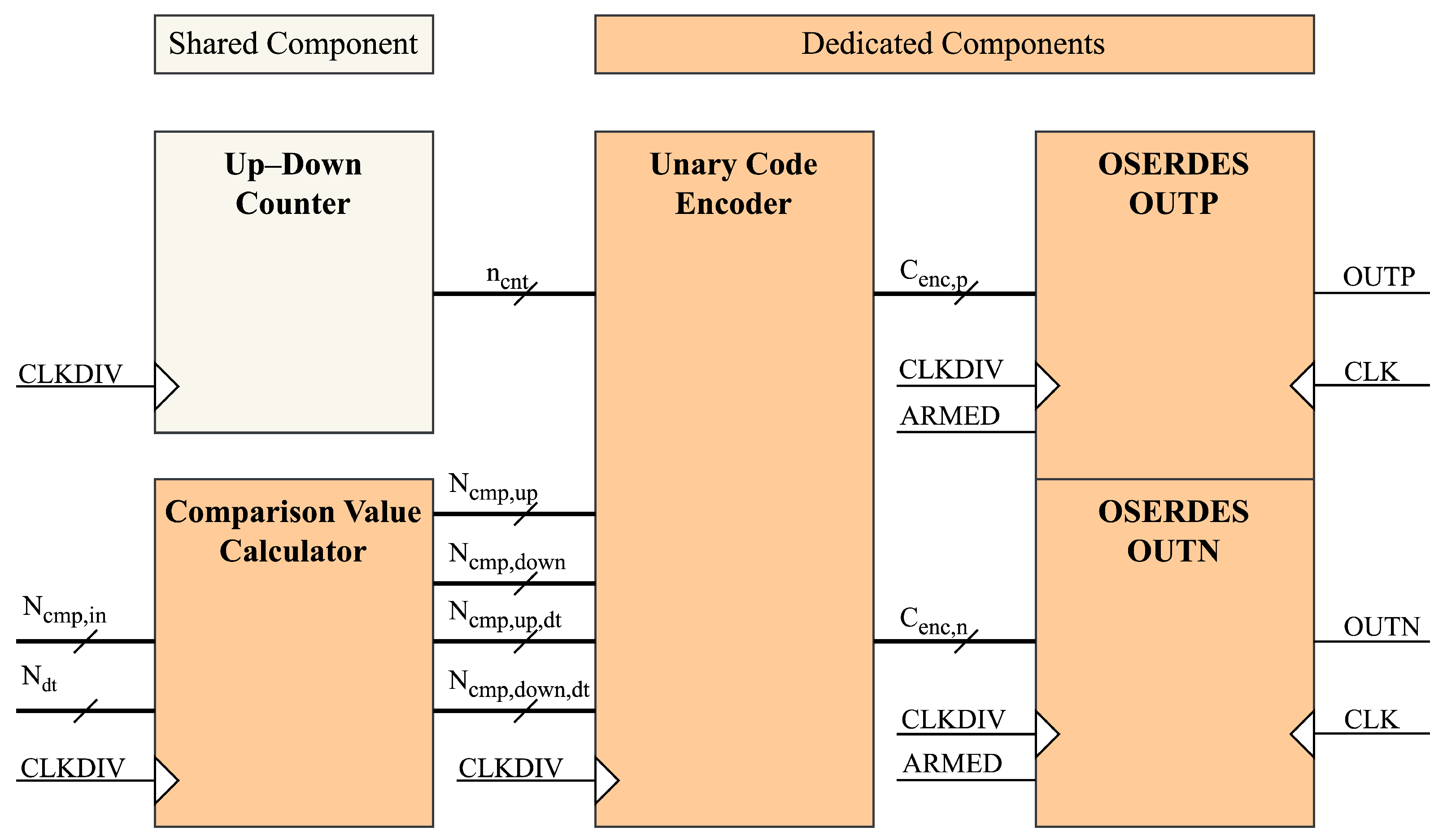
As shown in Figure 2, the proposed CA-HRPWM consists of four major components: the comparison value calculator, the up–down counter, the unary code encoder, and the OSERDES-based digital-to-time converter (DTC). The comparison value calculator restricts the input duty cycle command to prevent undefined behavior and generates the comparison value to drive the encoder. The up–down counter serves as the time base, defining the period and generating a triangular carrier for encoder operation. The unary code encoder, a key component of the design, determines the unary code of the actual PWM output based on the current counter value and comparison value. Finally, the OSERDES-based DTC converts the parallel unary code into a serial PWM output while integrating a fault trigger protection feature. Since all PWM channels require a common time base, the up–down counter is shared, while the other three components are dedicated to each pair of channels.
In this section, we describe how several bitwise operations are used to manipulate binary data. The logical left shift of a variable is denoted as variable n , where n represents the number of positions the bits are shifted to the left, with zeros filling in the shifted positions. Similarly, the logical right shift is represented as variable n , where the bits are shifted to the right by n positions, and zeros are inserted into the higher bits. A bit slice operation refers to extracting a range of bits from a variable, denoted as variable [ i : j ] , which selects bits from position j to position i. Lastly, the bitwise NOT operation, denoted as variable ¯ , inverts all the bits of the variable.

2.1. Comparison Value Calculator

The comparison value calculator receives the input duty command N c m p , i n from the source module and calculates the comparison values for the count-up and count-down processes, respectively. In conventional CA-PWM generation, the comparison values for both the count-up and count-down processes are identical. This results in half the resolution of an edge-aligned PWM under the same clock frequency, since a single-unit increase in the input comparison value leads to a two-unit variation in the duty cycle. To prevent this loss of resolution, the comparison value patterns ( N c m p , u p , N c m p , d o w n ) are restructured from ( 0 , 0 ) ( 1 , 1 ) ( 2 , 2 ) ( T p e r i o d / 2 , T p e r i o d / 2 ) to ( 0 , 0 ) ( 0 , 1 ) ( 1 , 1 ) ( 1 , 2 ) ( 2 , 2 ) ( T p e r i o d / 2 , T p e r i o d / 2 ) in the proposed design.
The comparison values N c m p , u p and N c m p , d o w n are calculated as
N c m p , u p = N c m p , i n 2 ,
N c m p , d o w n = N c m p , i n + 1 2 + 8 .
Note that the counter decrements from T p e r i o d 16 to one instead of zero, with each count corresponding to eight least significant bits (LSBs) in the comparison value. So, the + 8 in Equation (2) ensures proper OSERDES operation during the count-down process.
Considering dead time generation for active high complementary outputs, the rising edges of both outputs are delayed by N d t , while the falling edges stay the same. The delayed comparison values, N c m p , u p , d t and N c m p , d o w n , d t , can be derived from
N c m p , u p , d t = N c m p , u p + N d t ,
N c m p , d o w n = N c m p , d o w n N d t .
To avoid undefined behavior caused by data corruption near zero or a full duty cycle, the input data range must be limited based on the dead time N d t and PWM period T p e r i o d . The acceptable range is specified by
0 N c m p , u p , N c m p , u p , d t T p e r i o d 2 ,
8 N c m p , d o w n , N c m p , d o w n , d t T p e r i o d 2 + 8 .
The simplified lower limit B c m p , i n and upper limit U c m p , i n for N c m p , i n are as follows:
B c m p , i n = 2 N d t 1 ,
U c m p , i n = T p e r i o d 2 N d t .

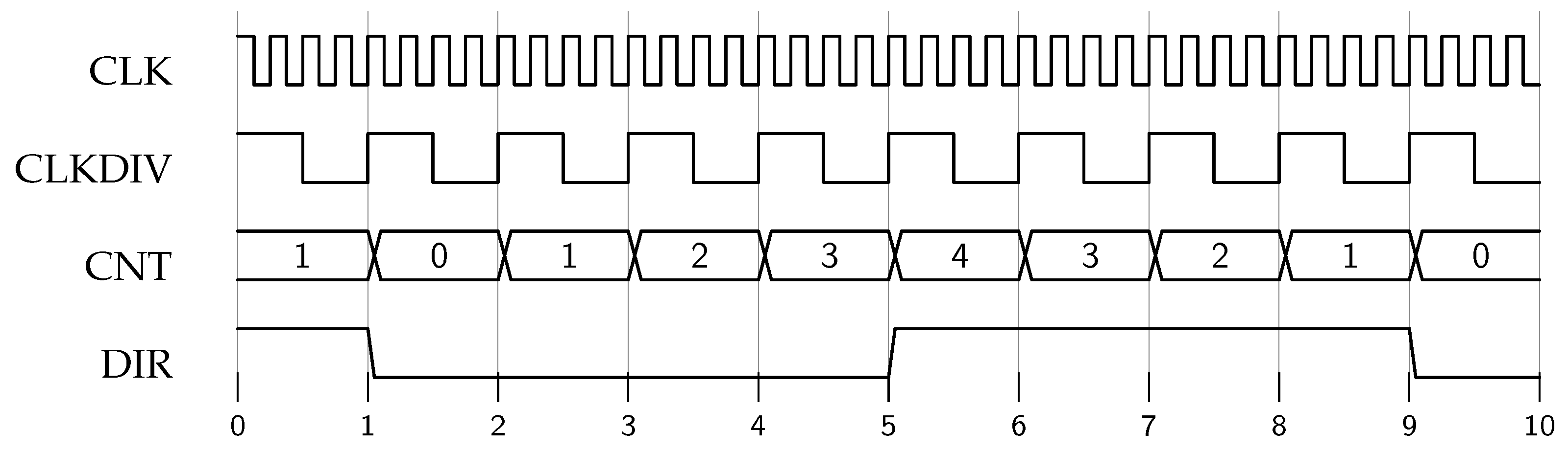
2.2. Up–Down Counter

The up–down counter value n c n t continuously increments from zero to T p e r i o d 16 1 , then decrements from T p e r i o d 16 to one, forming a triangular carrier that serves as a time base, as illustrated in Figure 3. To ensure proper operation, T p e r i o d must be a multiple of 16.

2.3. Unary Code Encoder

The unary code encoder takes the comparison values of all channels and splits them into two parts. The higher bits (most significant bits (MSBs) to three) are compared with the up–down counter value to determine when to activate the encoder. When the higher bits of the comparison value do not match the counter value, the encoder remains inactive, resulting in a constant output of either 0xFF or 0x00. This means the output stays entirely high or low during the counter clock period. When the higher bits of the comparison value match the counter value, the lower bits (two to zero) are encoded and fed into the OSERDES to fine-tune the output edge position.
For a positive output, when the counter is counting up, the output value C e n c , p is
C e n c , p = 0 x 00 , n c n t < N c m p , u p , d t [ MSB : 3 ] ,
C e n c , p = 0 xFF N c m p , u p , d t [ 2 : 0 ] , n c n t = N c m p , u p , d t [ MSB : 3 ] ,
C e n c , p = 0 xFF , n c n t > N c m p , u p , d t [ MSB : 3 ] .
Similarly, when the counter is counting down, the output value is
C e n c , p = 0 x 00 , n c n t < N c m p , d o w n [ MSB : 3 ] ,
C e n c , p = 0 xFF N c m p , d o w n [ 2 : 0 ] , n c n t = N c m p , d o w n [ MSB : 3 ] ,
C e n c , p = 0 xFF , n c n t > N c m p , d o w n [ MSB : 3 ] .
For a negative output, the output value is inverted, and the rising edge while counting down is delayed, giving the following output value, C e n c , n , when counting up:
C e n c , n = 0 xFF , n c n t < N c m p , u p [ MSB : 3 ] ,
C e n c , n = 0 xFF N c m p , u p [ 2 : 0 ] ¯ , n c n t = N c m p , u p [ MSB : 3 ] ,
C e n c , n = 0 x 00 , n c n t > N c m p , u p [ MSB : 3 ] .
Similarly, when the counter is counting down, the output value is
C e n c , n = 0 xFF , n c n t < N c m p , d o w n , d t [ MSB : 3 ] ,
C e n c , n = 0 xFF N c m p , d o w n , d t [ 2 : 0 ] ¯ , n c n t = N c m p , d o w n [ MSB : 3 ] ,
C e n c , n = 0 x 00 , n c n t > N c m p , d o w n , d t [ MSB : 3 ] .

2.4. OSERDES-Based DTC

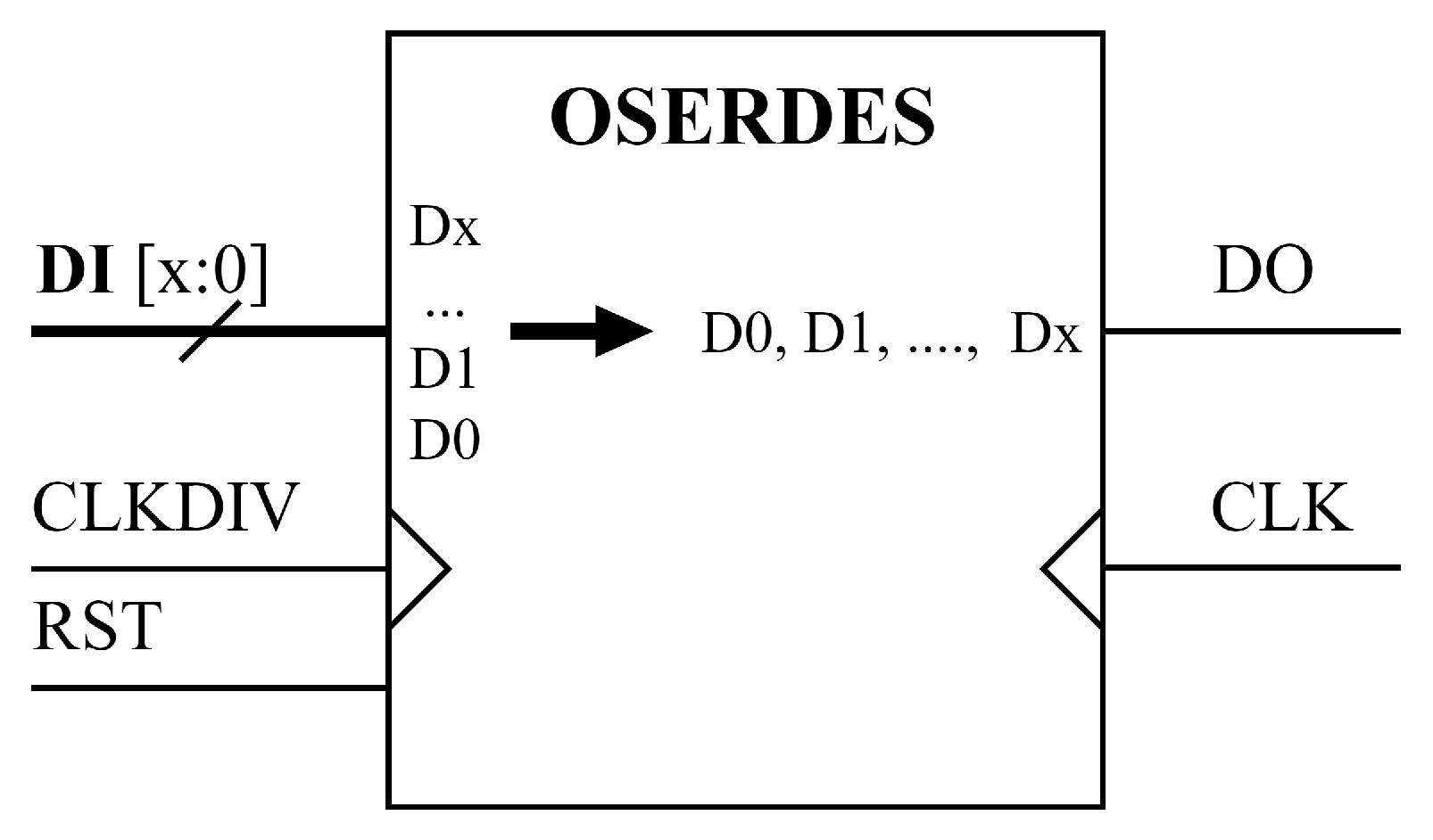
The OSERDES module in an FPGA is a dedicated parallel-to-serial converter designed to enable high-speed, source-synchronous interfaces. Figure 4 presents a simplified view of the OSERDES module. Each OSERDES module contains a serializer that converts parallel data from a low-speed clock domain into serial data. The least significant bit (LSB) of the input parallel data is serialized first, followed by the remaining more significant bits. The serializers can be configured in single-data-rate (SDR) or double-data-rate (DDR) mode, supporting data serialization ratios of up to 8:1 in DDR mode. The OSERDES module requires a reset before operation, and the output data are driven low when the reset input is asserted.
Aside from its primary use in high-speed interfaces, the OSERDES module can also function as a digital-to-time converter (DTC) when fed with the appropriate input vector. Each I/O tile contains a dedicated OSERDES module, ensuring that the OSERDES modules used on different pins do not interfere with one another, making them ideal for a multichannel output.
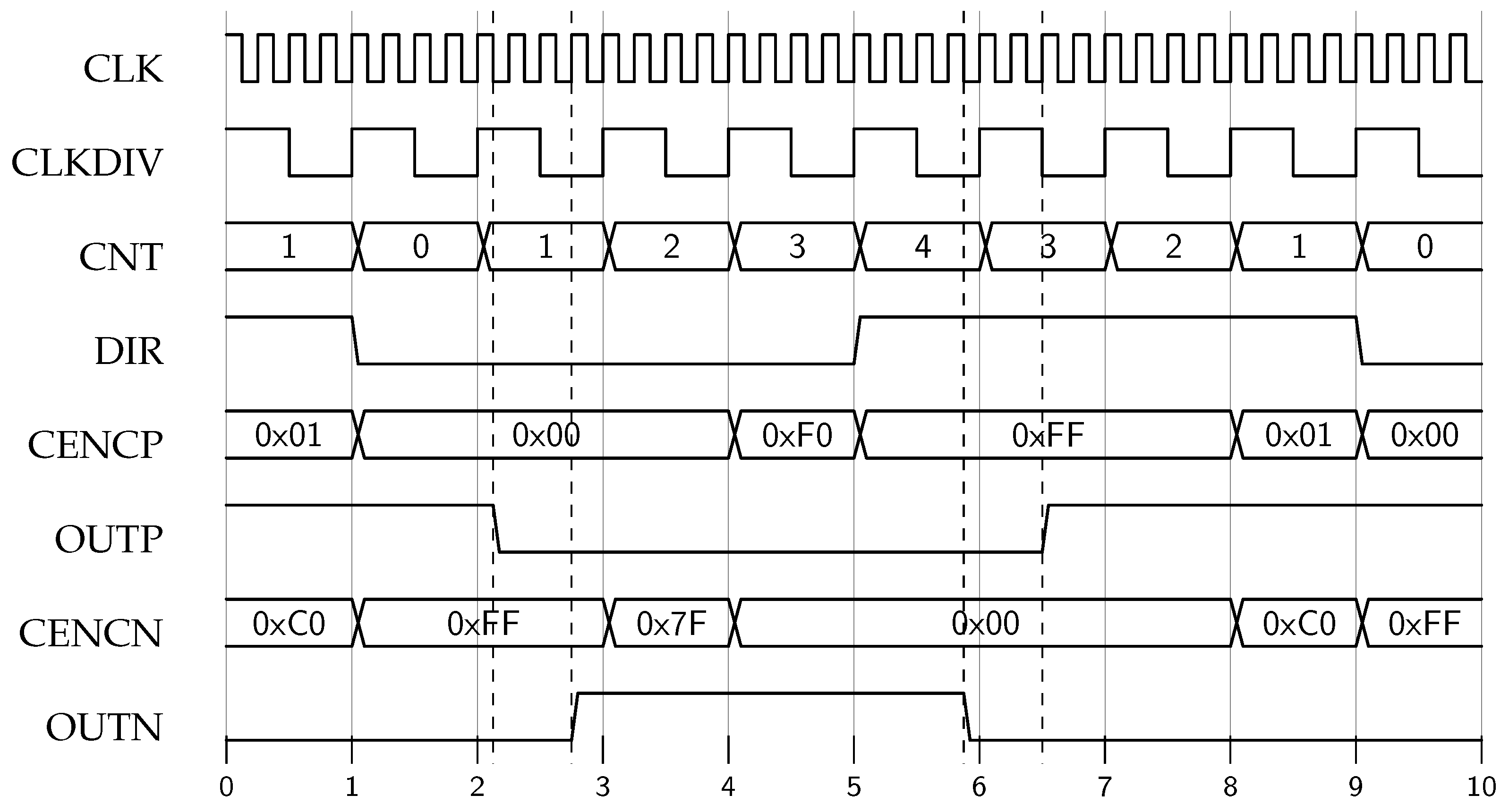
In the proposed design, the OSERDES operates as a DTC, serializing C e n c to form the actual CA-HRPWM signal, as shown in Figure 5. Note that the C e n c , p and C e n c , n are registered for one CLKDIV cycle to ensure that the timing constraints are met. Additionally, the internal delay of the OSERDES module is two CLKDIV cycles when operating in 8:1 DDR mode, resulting in a total delay of three CLKDIV cycles.
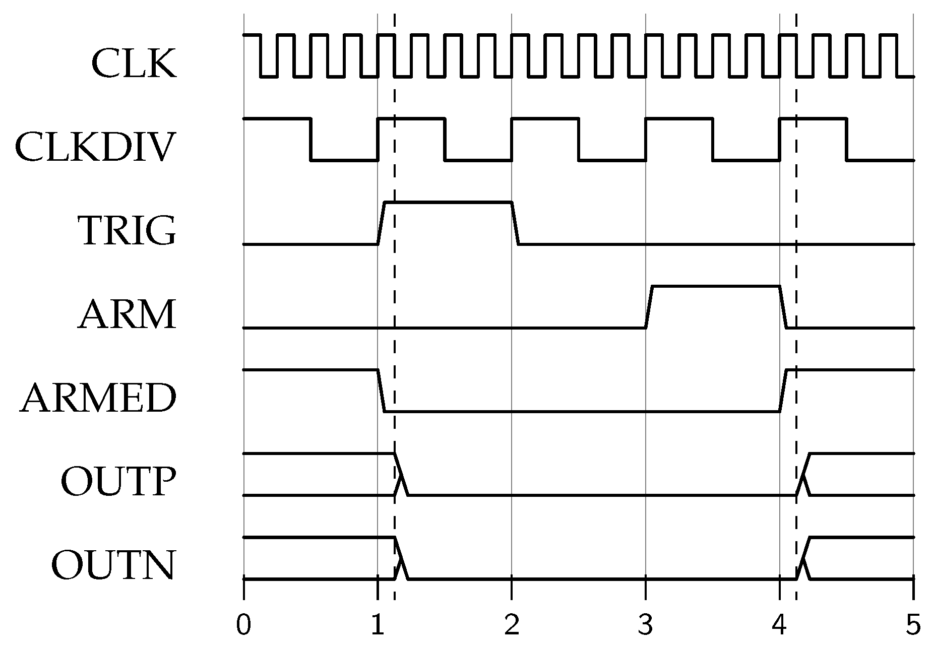
When the trigger port receives a failure signal indicating a fault condition like an overcurrent, the trigger signal is latched, and the OSERDES output is set to low after one CLK cycle. The output remains low for another CLK cycle after the arm signal arrives, which resets the triggered state to armed, as represented in Figure 6.

3. CA-HRPWM Simulation and Implementation

3.1. Software Simulation

To verify the functionality of the CA-HRPWM module, a simulation was performed using Xsim in Vivado 2023.2. To accelerate the simulation and demonstrate more timing details, the PWM period was set to 64. As shown in 
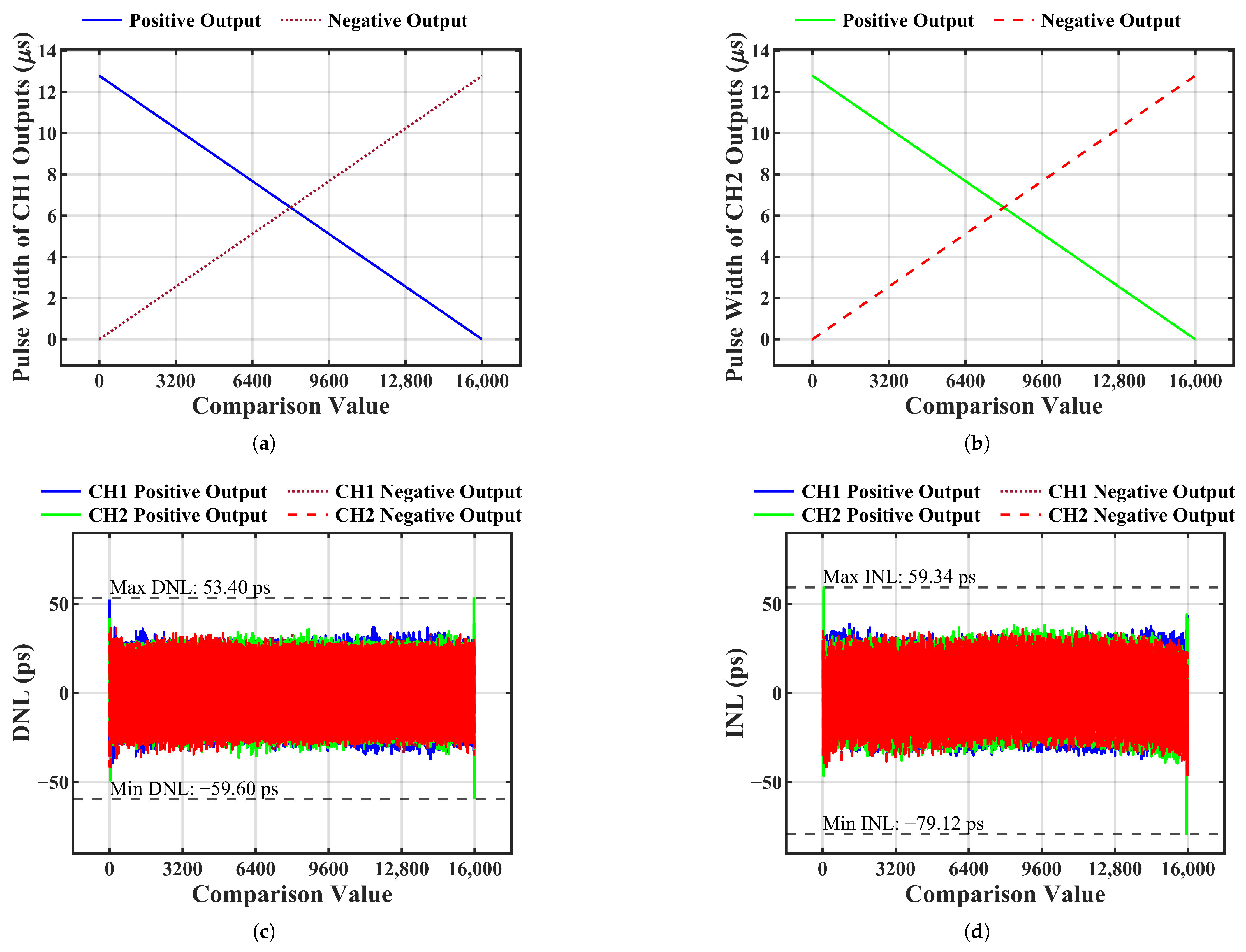
Figure 7, the dead time was correctly set to 4 ns, and the output pulse width accurately reflected the input comparison values.

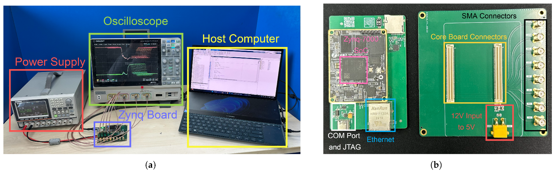
3.2. Hardware Implementation

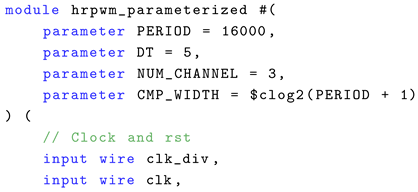
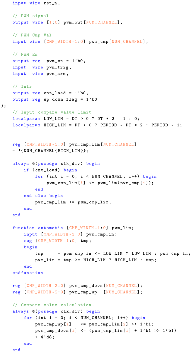
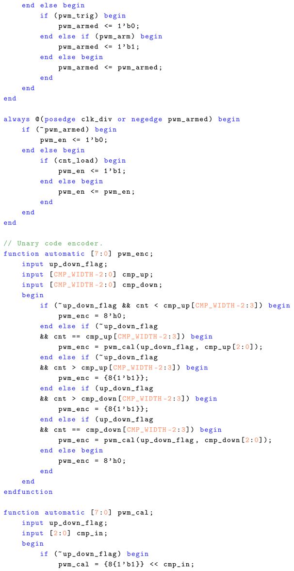
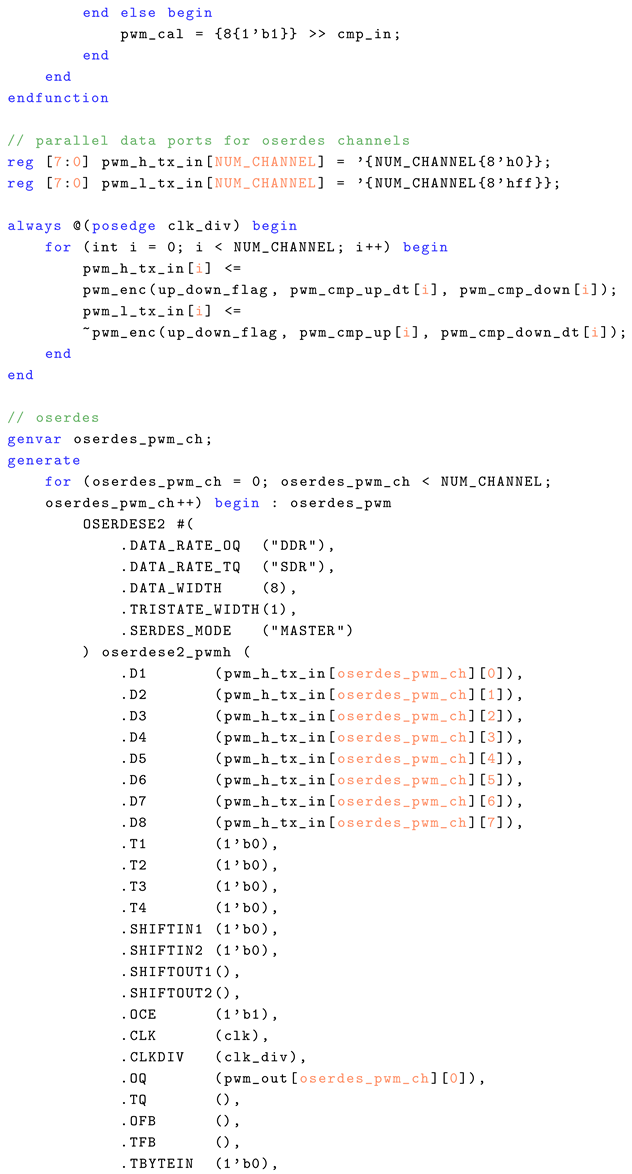
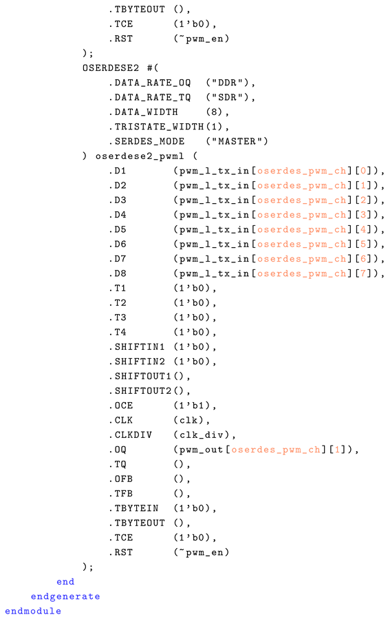
For a performance evaluation, the proposed CA-HRPWM was implemented on a Zynq-7000 SoC XC7Z020CLG400-2 (Xilinx, San Jose, CA, USA) using the Vivado 2023.2 EDA tool with the default settings. The Zynq-7000 SoC is an integration of two parts: programmable logic (PL) and a processing system (PS). The programmable logic is equivalent to any other Artix 7 series FPGA, and the processing system consists of dual ARM Cortex-A9 cores. The PL and PS have several Advanced eXtensible Interface (AXI) connections between them to perform data transfer. The proposed CA-HRPWM was implemented in hardware on the PL, while communication with the host computer and data loading to the CA-HRPWM module were managed by bare metal software running on the PS. The source code and the corresponding flowchart of the proposed CA-HRPWM are provided in Appendix A.
As for the timing parameters, the clock (CLK) frequency was set to 625 MHz, and the divided clock (CLKDIV) frequency was set to 156.25 MHz to achieve an optimal resolution. The PWM period and dead time were configured to 16,000 and 5, respectively, in accordance with the module parameters used in the experiments.
To evaluate the resource overhead of the proposed CA-HRPWM design, we implemented a conventional counter-based CA-PWM module with the same clock frequency, PWM period, dead time, and channel number configuration as the proposed design. The comparison module operated at 156.25 MHz, the same clock frequency as that of the CLKDIV in the HRPWM module. The corresponding resolution was 1 / 156.25 MHz = 6.4 ns , which was exactly eight times the 800 ps resolution of the HRPWM module. This allowed for a direct comparison of resource usage while maintaining identical functional behavior.
We also implemented the IODELAY-based CA-HRPWM design proposed in [20] for comparison. As noted in the Introduction, although its applicability is limited by the glitch-free input limitations of the IODELAY module, this design remains well suited for multichannel applications. The clock (CLK) operated at 390.625 MHz, while the reference clock (CLKREF) for delay chain calibration was set to 195.3125 MHz, ensuring compliance with device specifications and achieving an 80 ps resolution. Note that the 10-times-higher resolution achieved by the IODELAY-based method compared to our module benefits power supply applications, where switching frequencies could reach tens of megahertz. However, this level of resolution is unnecessary for PMSM control, as switching frequencies typically remain below 1 MHz.
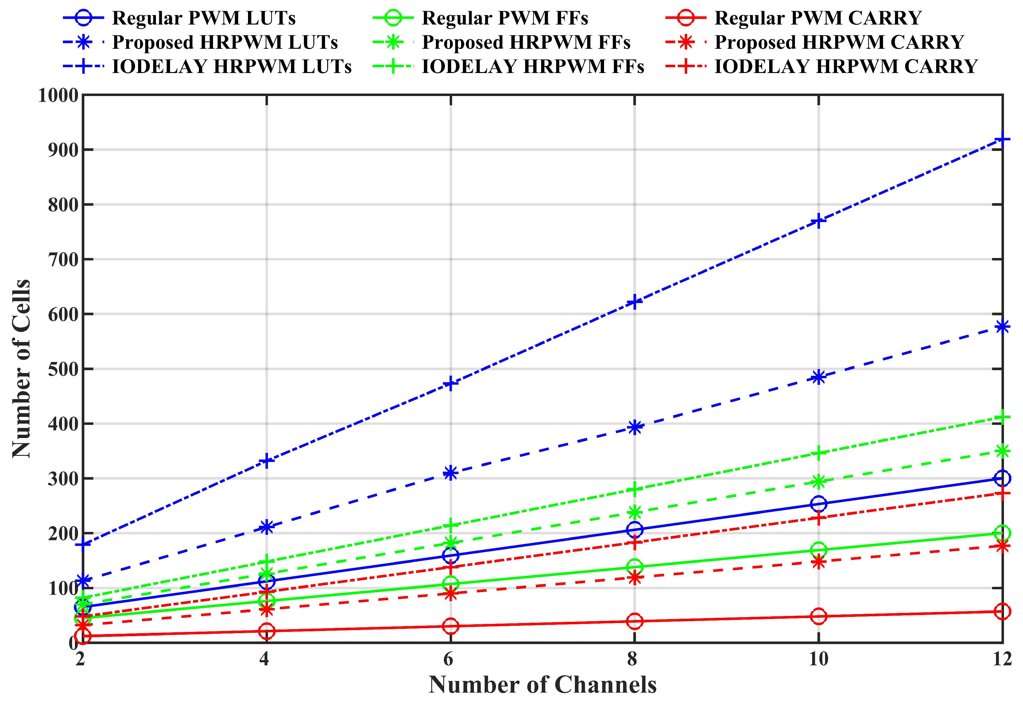
The slope of linear regression for the usage of lookup tables (LUTs), flip-flops (FFs), and carry chains (CARRY) per channel was used as a metric for resource utilization, as it quantifies the rate at which resource consumption increases with the number of channels. This approach provided a clear indication of how efficiently the proposed CA-HRPWM design scales as more channels are added.
The resource usage for configurations ranging from 2 to 12 channels is presented in Figure 8. The linear relationship between the number of cells and channels holds for both the proposed and comparison modules, confirming that the slope is a valid metric for the resource utilization per channel.
The average additional resource usage per channel for configurations ranging from 2 to 12 channels is shown in Table 2. The numbers of LUTs, FFs, and CARRY for each additional channel were 47, 28, and 15, respectively. These values were only 1.8 to 3.2 times as high as the resource usage of conventional CA-PWM implementations. Compared to the IODELAY-based CA-HRPWM, the values were further reduced by 15% to 36%. The XC7Z020CLG400-2 device provides 125 I/O ports in programmable logic (PL). Based on the results, we estimate that even with a maximum configuration of 125 channels, the total utilization rate of the resources would be approximately 14%. This demonstrates the high efficiency of the proposed CA-HRPWM design, which makes it well suited for multichannel applications.
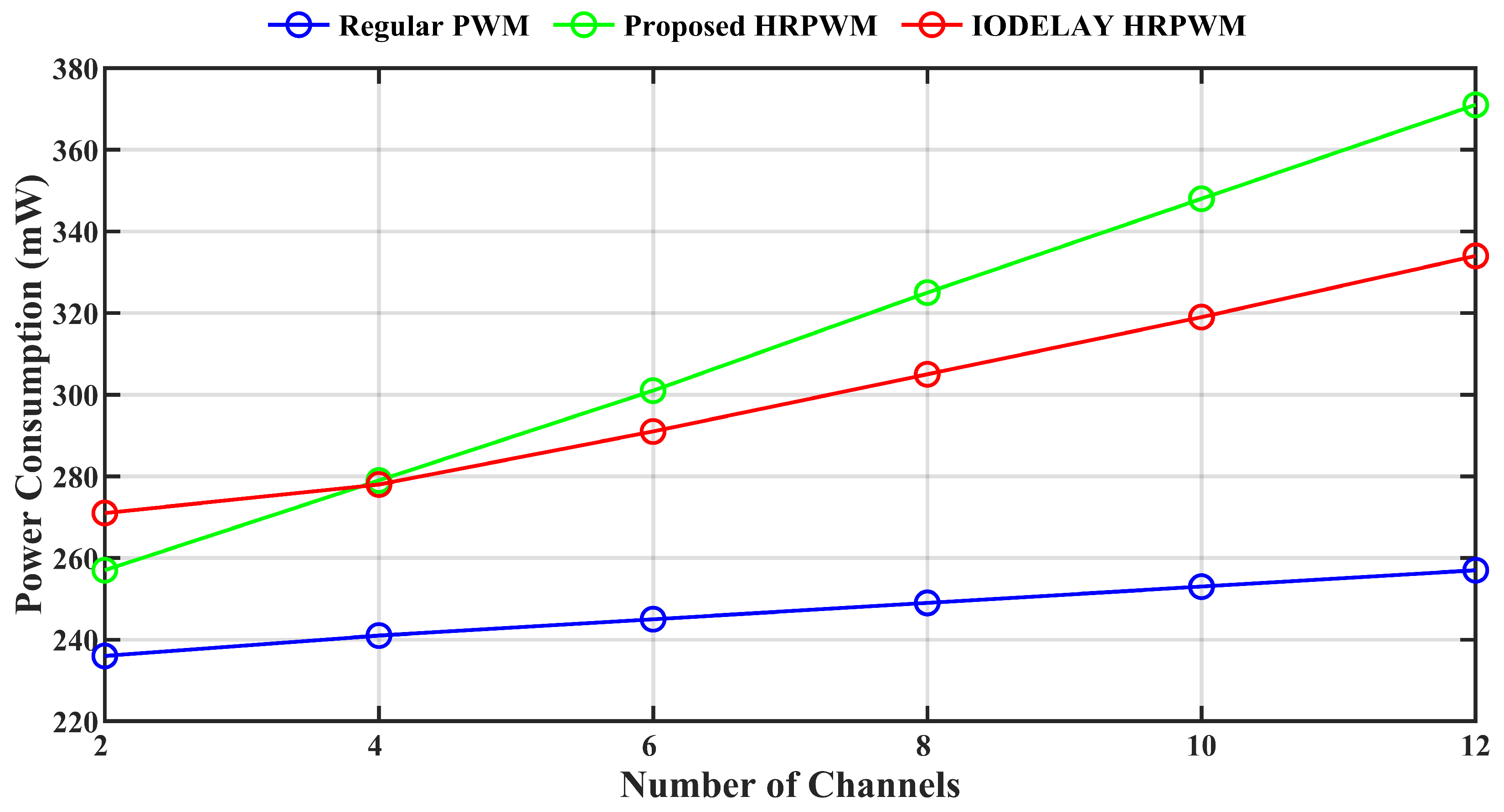
The power estimation for configurations ranging from 2 to 12 channels is presented in Figure 9, while the average additional power consumption per channel is detailed in Table 3. For the proposed design, the extra power consumption per channel was 5.4 times that of a conventional CA-PWM and 1.8 times of the IODELAY-based CA-HRPWM. Despite this increase, the power consumption remains acceptable for PMSM control applications, as the motor itself operates within a power range of tens to thousands of watts.

4. Experimental Results

To validate the proposed CA-HRPWM design, two experiments were conducted. The first experiment evaluated the pulse width resolution, dead time accuracy, and overall functionality of the CA-HRPWM module by measuring its output signals using an oscilloscope. The second experiment demonstrated the impact of the CA-HRPWM on the motor current ripple by implementing it in a PMSM field-oriented control (FOC) system. The current response was compared between a conventional PWM and the proposed CA-HRPWM to quantify the reduction in the current ripple.

4.1. Pulse Measurement

A Siglent SDS6104 H10 Pro oscilloscope, with a 1 GHz bandwidth and a 5 GSPS sample rate, was used to directly measure the pulse output. Figure 10 shows the setup for the pulse measurement. The CA-HRPWM output signal was routed from the Zynq core board to a test jig equipped with SMA connectors. From there, the signals passed through a coaxial cable to the BNC connector on the oscilloscope panel for measurement and analysis. The output pulse width of the CA-HRPWM was controlled by the host computer via the COM port, while the trigger and measurement readback of the oscilloscope were managed using SCPI instructions given through a USB.
Figure 11 shows the time lapse of 5000 pulses with 16 consecutive comparison values for N c m p , i n ranging from 9 to 24, with the period set to 16,000 and the dead time N d t set to 5. Each step corresponded to 800 ps, so the cycle was T p e r i o d = 16000 × 800 ps = 1.28 μ s and the dead time was N d t = 5 × 800 ps = 4 ns . The measured 800 ps pulse width resolution, 4 ns dead time, and 78.12451 kHz frequency, verified by both the cursor and the hardware frequency meter, confirmed the proper functionality of the module and validated its high-resolution performance.
To further demonstrate the linearity of the proposed CA-HRPWM, the pulse width of both the positive and negative channels was measured across the full input range from 0 to 16,000 with an interval of 1. As shown in Figure 12, the DNL was within −59.60 ps to +53.40 ps, and the INL was within −79.12 ps to +59.34 ps. The jitter of the pulse width was characterized by the RMS value calculated from 100 samples for each comparison value. The maximum jitter was 31.7 ps RMS.
The linear regression results are summarized in Table 4. Specifically, the coefficient of determination R 2 deviated by only 19 parts per trillion (ppt) from 1, exceeding the 99.999% linearity reported in [16,20]. Additionally, the highest root mean square error (RMSE) was 16.066 ps, outperforming the 20.5 ps reported in [16]. These results validate the excellent linearity of the proposed CA-HRPWM implementation.

4.2. PMSM Current Control

A PMSM current controller was implemented using the proposed CA-HRPWM to demonstrate its benefits in current control, compared to a conventional PWM generator. Figure 13 shows the setup for the PMSM current controller, and the motor electrical parameters are listed in Table 5. The motor was driven by a three-phase voltage source inverter (VSI), with the power stage consisting of three ISG3201 GaN half-bridge modules that integrated gate drivers and bootstrap diodes. The proposed CA-HRPWM generated three pairs of active high complementary PWM signals, which drove the inverter for effective current regulation. The current was measured using three 40 mΩ shunt resistors in line and converted by three TI AMC3306M25 isolated delta–sigma modulators. Each AMC3306M25 modulator output a 20 MHz delta–sigma bitstream, which was synchronously sampled by the FPGA and processed using a 256th-order Sinc3 CIC filter. The input DC voltage was set to 48 V. The PWM frequency and dead time were configured to 78.125 kHz and 4 ns, respectively, throughout the experiment. The HR-CAPWM clock configuration was set to 156.25 MHz for CLKDIV and 625 MHz for CLK, and the resolution was 800 ps. Current readings and other parameters were transmitted to the host computer via Ethernet at a sampling rate of 40 kSPS.
The PMSM current controller used in this study was a field-oriented control (FOC) PI controller. As shown in Figure 14, the PI current controller was implemented in the synchronous reference frame for both direct and quadrature currents. To demonstrate the impact of the proposed CA-HRPWM on the current ripple, PWM generation in the experiment was performed using both the conventional method and the proposed CA-HRPWM, while all other components of the current controller remained unchanged.
The PI current controller is represented as
U q = K p ( I q , r e f I q ) + K i 0 t ( I q , r e f I q ) d t ,
U d = K p ( I d , r e f I d ) + K i 0 t ( I d , r e f I d ) d t ,
where I d , r e f and I q , r e f are the direct and quadrature axis current commands, respectively, and I d and I q are the corresponding measured currents.
The proportional and integral gains K p and K i were set as
K p = L s / ( 3 · T s ) = 11.849 ,
K i = R s / ( 3 · T s ) = 3081.6 ,
where L s , R s , and T s are the stator inductance, stator resistance, and current sampling period, respectively.
In the experiment, the direct axis current command I d , r e f was set to a constant zero for simplicity, as the rotor was non-salient, while the quadrature axis current command I q , r e f was provided by the host computer to generate electromagnetic torque. Figure 15 shows the measured quadrature axis current I q in response to a 5 Hz sine command with an amplitude of 10 mA and a 30 mA offset, both before and after the CA-HRPWM was enabled. With the proposed CA-HRPWM, the maximum peak-to-peak current ripple I p p was reduced from 4 mA to 2 mA, which represents a 50% reduction in the current ripple compared to a conventional PWM generator.
To further evaluate the current controller across a broader operating range, we measured I q responses to commands from 100 mA to 500 mA. As shown in Table 6, the current ripple reduction achieved by the proposed CA-HRPWM ranged from 46% to 64% compared to a conventional PWM generator.
This outcome highlights the effectiveness of the proposed CA-HRPWM in minimizing current fluctuations, which is beneficial for applications requiring precise torque control. A reduction in the current ripple could be helpful to achieving smoother motor operation, lower acoustic noise, and enhanced efficiency. The proposed design has proved its ability to improve the performance of the PMSM current controller, making it an ideal choice for high-performance drive systems.

5. Conclusions

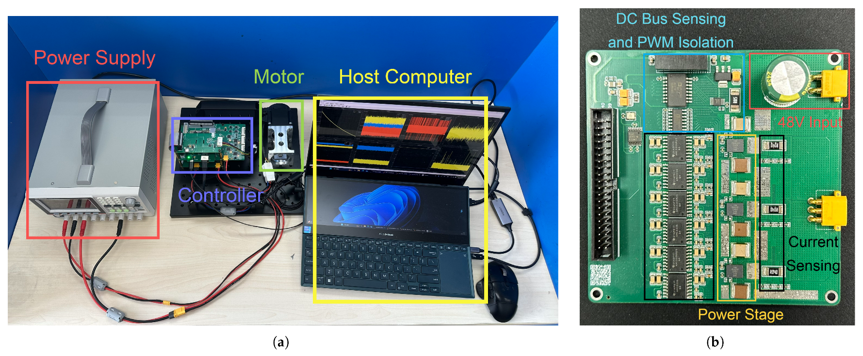
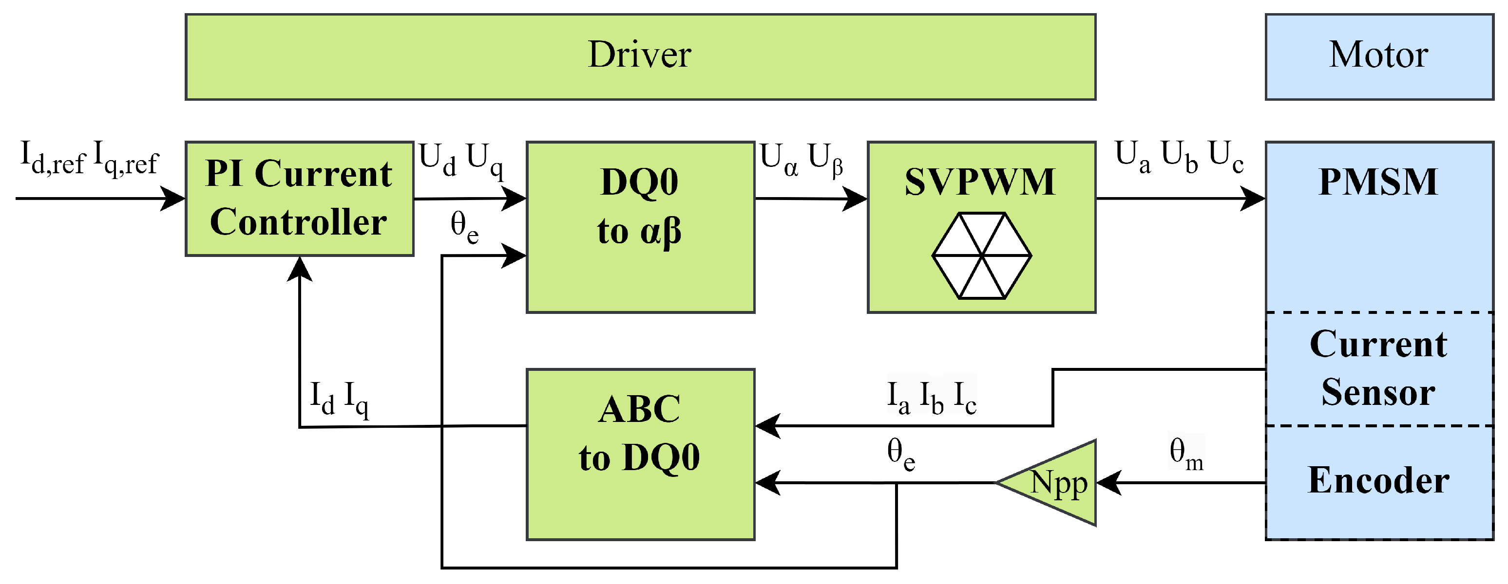
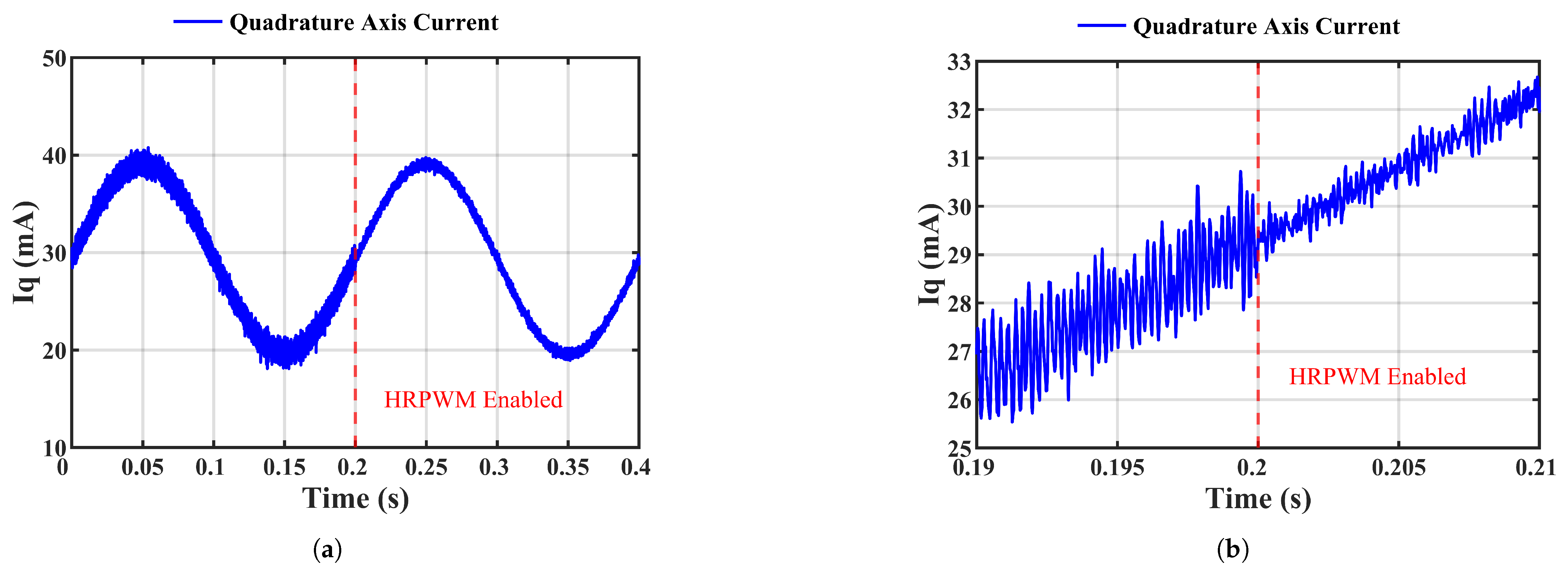
In this paper, we proposed a center-aligned high-resolution PWM (CA-HRPWM) implementation based on the OSERDES module in FPGAs. The design leverages the OSERDES module as a digital-to-time converter (DTC), achieving high-resolution pulse generation with minimal resource utilization and ideal linearity, making it suitable for multichannel applications. The experimental results demonstrate that the proposed CA-HRPWM achieved a resolution of 800 ps with low jitter and high linearity. It also significantly improved the current control performance, reducing the current ripple by up to 64% compared to a conventional PWM generator. This approach offers a promising solution for high-performance multichannel CA-PWM generation in FPGA-based power electronic systems, with potential applications in motor control, DC-DC converters, and other digital power systems.
To further enhance the performance and broaden the potential applications, future research may focus on supporting diverse PWM waveforms for various power electronic systems and integrating the proposed method with IODELAY on specific FPGAs to achieve a higher time resolution.

Supplementary Materials

The following supporting information can be downloaded at: https://www.mdpi.com/article/10.3390/act14040181/s1, Table S1: Pulse measurement raw data.

Author Contributions

Conceptualization, Z.W.; methodology, Y.W.; validation, Y.W.; writing—original draft preparation, Y.W. and Z.W. All authors have read and agreed to the published version of the manuscript.

Funding

This research received no external funding.

Data Availability Statement

The original contributions presented in this study are included in the article/Supplementary Material. Further inquiries can be directed to the corresponding author.

Acknowledgments

We would like to thank SIGLENT Technologies (https://www.siglent.com/) for providing the oscilloscope used for pulse measurement.

Conflicts of Interest

The authors declare no conflicts of interest.

Appendix A

The SystemVerilog code and the corresponding flowchart of the proposed CA-HRPWM implementation are shown below.
  • Listing A1. Source code of CA-HRPWM.
Actuators 14 00181 i001Actuators 14 00181 i002Actuators 14 00181 i003Actuators 14 00181 i004Actuators 14 00181 i005Actuators 14 00181 i006
Figure A1. High-level flowchart of CA-HRPWM module.
Actuators 14 00181 g0a1

References

  1. van der Broeck, H.; Skudelny, H.C.; Stanke, G. Analysis and Realization of a Pulsewidth Modulator Based on Voltage Space Vectors. IEEE Trans. Ind. Appl. 1988, 24, 142–150. [Google Scholar] [CrossRef]
  2. Hesener, A. GaN Power ICs Drive Efficiency and Size Improvements in BLDC Motor Drive Applications. In Proceedings of the PCIM Europe 2023; International Exhibition and Conference for Power Electronics, Intelligent Motion, Renewable Energy and Energy Management, Nuremberg, Germany, 9–11 May 2023; pp. 1–6. [Google Scholar] [CrossRef]
  3. Peterchev, A.; Sanders, S. Quantization Resolution and Limit Cycling in Digitally Controlled PWM Converters. IEEE Trans. Power Electron. 2003, 18, 301–308. [Google Scholar] [CrossRef]
  4. Peng, H.; Prodic, A.; Alarcon, E.; Maksimovic, D. Modeling of Quantization Effects in Digitally Controlled DC–DC Converters. IEEE Trans. Power Electron. 2007, 22, 208–215. [Google Scholar] [CrossRef]
  5. Texas Instruments. TMS320F2837xD Dual-Core Real-Time Microcontrollers; Texas Instruments: Dallas, TX, USA, 2024. [Google Scholar]
  6. Texas Instruments. F29H85x and F29P58x Real-Time Microcontrollers; Texas Instruments: Dallas, TX, USA, 2025. [Google Scholar]
  7. Ge, L.S.; Chen, Z.X.; Chen, Z.J.; Liu, Y.F. Design and Implementation of a High Resolution DPWM Based on a Low-Cost FPGA. In Proceedings of the 2010 IEEE Energy Conversion Congress and Exposition, Atlanta, GA, USA, 12–16 September 2010; pp. 2306–2311. [Google Scholar] [CrossRef]
  8. Kwiatkowski, P. Digital-to-Time Converter for Test Equipment Implemented Using FPGA DSP Blocks. Measurement 2021, 177, 109267. [Google Scholar] [CrossRef]
  9. Yu, L.; Xu, S.; Zhang, H.; Shi, L.; Sun, W. Design and Implementation of a Hybrid DPWM under 50 Ps Resolution Based on General-Purpose FPGA. Int. J. Circuit Theory Appl. 2021, 49, 114–127. [Google Scholar] [CrossRef]
  10. Chen, P.; Chen, P.Y.; Lai, J.S.; Chen, Y.J. FPGA Vernier Digital-to-Time Converter With 1.58 Ps Resolution and 59.3 Minutes Operation Range. IEEE Trans. Circuits Syst. Regul. Pap. 2010, 57, 1134–1142. [Google Scholar] [CrossRef]
  11. Wang, H.; Zhang, M.; Liu, Y. High-Resolution Digital-to-Time Converter Implemented in an FPGA Chip. Appl. Sci. 2017, 7, 52. [Google Scholar] [CrossRef]
  12. Yan, C.; Hu, C.; Wu, J. A High Resolution Vernier Digital-to-Time Converter Implemented with 65 Nm FPGA. Appl. Sci. 2019, 9, 2705. [Google Scholar] [CrossRef]
  13. Zeng, J.; Xu, J. A High-Precision Programmable Voltage Source Based on Vernier PWM. IEEE Trans. Instrum. Meas. 2024, 73, 2007910. [Google Scholar] [CrossRef]
  14. de León, I.; Sotta, G.; Eirea, G.; Pérez Acle, J. Analysis and Implementation of Low-Cost FPGA-based Digital Pulse-Width Modulators. In Proceedings of the 2014 IEEE International Instrumentation and Measurement Technology Conference (I2MTC) Proceedings, Montevideo, Uruguay, 12–15 May 2014; pp. 1523–1528. [Google Scholar] [CrossRef]
  15. Cheng, K. Implementation of High Resolution Digital Pulse Width Modulator Based on FPGA. In Proceedings of the 2019 IEEE International Conference on Signal, Information and Data Processing (ICSIDP), Chongqing, China, 11–13 December 2019; pp. 1–5. [Google Scholar] [CrossRef]
  16. Xu, B.; Xu, Q.; Guo, P.; Jia, Y.; Chen, Y.; Luo, A. High-Resolution Digital PWM Optimization Method for Critical Path Delay in General FPGA. CPSS Trans. Power Electron. Appl. 2024, 9, 190–206. [Google Scholar] [CrossRef]
  17. Kong, D.; Fu, Z.; Deng, Y.; Wang, R. A Reconfigurable Calibration-Free Digital-to-Time Converter Based on a High-Speed Transceiver. IEICE Electron. Express 2024, 22, 20240705. [Google Scholar] [CrossRef]
  18. Fernandez-Gomez, M.; Fernandez, C.; Zumel, P.; Sanchez, A.; Castro, A.D. Design of DPWM with High Resolution under 80 Ps Using Low-Cost Xilinx FPGA. In Proceedings of the 2020 IEEE Applied Power Electronics Conference and Exposition (APEC), New Orleans, LA, USA, 15–19 March 2020; pp. 3043–3048. [Google Scholar] [CrossRef]
  19. Fernandez-Gomez, M.; Sanchez, A.; de Castro, A.; Lopez-Lopez, J.; Zumel, P.; Fernandez, C. Design and Implementation of Two Hybrid High Frequency DPWMs Using Delay Blocks on FPGAs. IEEE Trans. Power Electron. 2021, 36, 14567–14578. [Google Scholar] [CrossRef]
  20. Hajiheidari, M.; Fushekati, J.; Emad, M.; Vermulst, B.J.D.; van Duivenbode, J.; Huisman, H. Single-Path High-Resolution Digital PWM Architectures With Cascadability of Delay Lines. IEEE Open J. Power Electron. 2025, 6, 130–143. [Google Scholar] [CrossRef]
Figure 1. Timing diagram of three-phase center-aligned PWM and current sampling window.
Actuators 14 00181 g001
Figure 2. Block diagram of proposed CA-HRPWM module.
Actuators 14 00181 g002
Figure 3. Timing diagram of proposed up–down counter ( T p e r i o d = 64 ) .
Actuators 14 00181 g003
Figure 4. Simplified diagram of OSERDES module.
Actuators 14 00181 g004
Figure 5. Timing diagram of unary code encoder and OSERDES ( T p e r i o d = 64 , N c m p , i n = 30 , and N d t = 5 ).
Actuators 14 00181 g005
Figure 6. Timing diagram of trigger and arm ports.
Actuators 14 00181 g006
Figure 7. CA-HRPWM simulation waveform ( T p e r i o d = 64 , N c m p , i n = 29 , 30 , 31 , 32 , and N d t = 5 ).
Actuators 14 00181 g007
Figure 8. Resource usage of different channel configurations.
Actuators 14 00181 g008
Figure 9. Power consumption of different channel configurations.
Actuators 14 00181 g009
Figure 10. Experimental setup for direct pulse measurement. (a) Overview of test equipment. (b) Details of Zynq core board and test jig.
Actuators 14 00181 g010
Figure 11. The oscilloscope measured results for 16 consecutive fine duty cycle steps. Positive and negative outputs were captured on oscilloscope channel 1 and channel 3, respectively.
Actuators 14 00181 g011
Figure 12. Pulse width characteristics of 2 different pairs of channels. (a) Pulse width of channel 1. (b) Pulse width of channel 2. (c) Pulse width differential nonlinearity (DNL). (d) Pulse width integral nonlinearity (INL).
Actuators 14 00181 g012
Figure 13. Experimental setup for PMSM current controller. (a) Overview of test equipments. (b) Details of power board.
Actuators 14 00181 g013
Figure 14. Diagram of PMSM field-oriented control.
Actuators 14 00181 g014
Figure 15. Measured quadrature axis current ( I q ). (a) I q before and after HRPWM was enabled. (b) Zoomed-in time scale.
Actuators 14 00181 g015
Table 1. FPGA-based HRPWM implementation comparison.
MethodResource UtilizationExternal Circuitry RequirementsResolutionCA-PWM CapabilityCalibration RequirementsSystem Timing
Tapped delay chain [7,8,9]HighNoHighYesYesAsync
Vernier [10,11,12,13]LowDevice-specificVery highNoNoAsync
Multiphase clocking [14,15,16]MediumNoMediumYesNoSync
High-speed transceiver [17]LowYesHighYesNoSync
IODELAY [18,19,20]LowNoHighDevice-specificNoSync
OSERDES [14]LowNoMediumYesNoSync
Table 2. Resource usage per additional channel of conventional CA-PWM, IODELAY-based CA-HRPWM, and proposed CA-HRPWM.
MethodLUTsFFsCARRY
CA-PWM24165
IODELAY-Based CA-HRPWM (Overhead)74 (+50)33 (+17)23 (+18)
Proposed CA-HRPWM (Overhead)47 (+23)28 (+12)15 (+10)
Table 3. Power consumption per additional channel of conventional CA-PWM, IODELAY-based CA-HRPWM, and proposed CA-HRPWM.
MethodPower
CA-PWM2.1 mW
IODELAY-Based CA-HRPWM (Overhead)6.5 mW
Proposed CA-HRPWM (Overhead)11.4 mW
Table 4. Summary of linear regression results ( y = p 1 · x + p 2 ).
Channelp1p2R2RMSE
CH1P−800.01 ps12.796 μs1−19 ppt16.066 ps
CH1N800.00 ps−4.1226 ns1−12 ppt12.735 ps
CH2P−800.01 ps12.796 μs1−19 ppt16.024 ps
CH2N800.00 ps−4.1302 ns1−19 ppt15.785 ps
Table 5. Electrical parameters of the PMSM (model: TSM3005N2357E600 by Tamagawa seiki).
ParametersValue
Pole pairs ( N p p )5
Line inductance ( L p p )1.21 mH
Line resistance ( R p p )0.47 Ω
Torque constant ( T e )0.0997 N·m/A (RMS)
Rated power ( P r )200 W
Table 6. Summary of I q ripple.
Current CommandCA-PWMCA-HRPWMRipple Reduction
100 mA2.8 mA1.5 mA46%
200 mA4.4 mA1.5 mA64%
300 mA4.1 mA1.7 mA59%
400 mA4.0 mA1.6 mA60%
500 mA4.3 mA1.9 mA56%
Disclaimer/Publisher’s Note: The statements, opinions and data contained in all publications are solely those of the individual author(s) and contributor(s) and not of MDPI and/or the editor(s). MDPI and/or the editor(s) disclaim responsibility for any injury to people or property resulting from any ideas, methods, instructions or products referred to in the content.

