Article

Comparative Experimental Study on the De-Icing Performance of Multiple Actuators

National Key Lab of Aerospace Power System and Plasma Technology, Air Force Engineering University, Xi’an 710038, China
*
Author to whom correspondence should be addressed.
Actuators 2024, 13(6), 226; https://doi.org/10.3390/act13060226
Submission received: 2 April 2024 / Revised: 6 June 2024 / Accepted: 12 June 2024 / Published: 17 June 2024

Abstract

:
The issue of aircraft icing poses a substantial threat to flight safety. In order to investigate more efficient anti-icing and de-icing technologies, a comparative analysis was conducted on the de-icing characteristics of three types of actuator materials under varying conditions. Initially, experimental research was undertaken to analyze the temperature traits of three actuators under ice-free conditions. Three power densities were chosen for the experiment: 0.170 W/cm2, 0.727 W/cm2, and 1.427 W/cm2. The research findings revealed distinct characteristics: plasma actuators and resistance wire actuators exhibited a strip-like high-temperature region during operation, with well-defined boundaries between the high-temperature and low-temperature zones, whereas ceramic-based semiconductor actuators showcased a uniform high-temperature region. As energy consumption rose, the thermal equilibrium temperatures of all three types tended to converge, with resistance wire actuators operating at 1.427 W/cm2, showing the highest temperature rise rate at that power density. Subsequently, experimental research was carried out on the de-icing performance of three actuators under icing conditions at a specific power density. Following 120 s of de-icing, the ice layer covering the surface of the plasma actuator completely melted, forming a cavity. Conversely, the ice layer on the ceramic-based semiconductor actuator remained partially intact in a strip shape. Ice deposits were still visible on the surface of the resistance wire actuator. This observation highlights the remarkable de-icing speed of the plasma actuator. The propulsive force of plasma generated on the fluid inside the ice layer enhances heat transfer efficiency, thereby accelerating the de-icing process of the plasma actuator at the same power density. The analysis of the de-icing performance of these three novel types of actuators establishes a robust groundwork for exploring more effective aircraft de-icing methods. Furthermore, it furnishes theoretical underpinning for the advancement of composite anti-icing and de-icing strategies.

1. Introduction

Supercooled water droplets within cloud layers collide with aircraft surfaces and promptly freeze as the aircraft traverses frozen cloud [1,2]. Aircraft icing commonly manifests on the windward side, impacting critical areas such as engine lips, wing leading edges, and sensor surfaces, thereby significantly jeopardizing flight safety. The accrual of ice at the engine lip can diminish the intake cross-sectional area, affecting engine thrust and potentially culminating in engine failure [3]. Cockpit glass icing directly impairs pilot visibility, escalating flight complexity and the likelihood of error and accidents [4]. The formation of ice on the wing’s leading edge alters aerodynamic performance [5], underscoring the pivotal role of aircraft anti-icing/de-icing research in the realm of aviation. Specialists and scholars have recently been engaged in continuous simulations and calculations of the ice formation induced by aircraft flying under icing conditions [6,7,8,9].
De-icing methods, hinging on energy input, comprise mechanical and thermal approaches. Mechanical techniques such as expansion tubes and electric pulse de-icing exhibit distinct merits and demerits [10,11]. The prevalent hot gas de-icing technique involves channeling high-temperature gas from the engine to susceptible icing areas. While novel layout techniques are continually proposed, challenges like intricate pipeline arrangement and elevated energy consumption persist [12,13,14,15,16]. Electric de-icing devices, which convert electrical energy into thermal energy, are gaining prominence for their efficiency and ease of operation [17,18]. These devices curtail ice adhesion and facilitate ice removal through aerodynamic and centrifugal forces, propelling ongoing advancements in electric heating de-icing actuators.
Recent strides in composite materials have ignited exploration into electric heating actuators predicated on innovative materials [19,20,21,22,23,24,25]. For instance, graphene composite materials evince potential in de-icing wind turbine blades [26], whereas the amalgamation of electric heating coatings with superhydrophobic materials yields energy-efficient anti-icing coatings with industrial applications [27]. The examination of new electric heating materials encompasses ceramic-based semiconductor actuators [28], offering high thermal conversion rates, customizable heating areas, and improved hydrophobic qualities for aircraft de-icing applications. Amidst the quest for fresh electric heating materials, one of the substances employed in this experiment is a novel ceramic-based semiconductor actuator. This material boasts a high electric thermal conversion rate, uniform heating distribution, adaptable heating area configuration, consistent heating distribution, and commendable hydrophobic attributes. Additionally, the coating can alter its curvature with different substrate materials, enhancing its applicability in the domain of aircraft de-icing.
In recent years, extensive research has been conducted on the microscopic and macroscopic aspects of plasma through experimental and simulation methods [29,30,31,32,33,34,35]. It has been discovered that plasma not only has the effect of disturbing flow [36,37,38,39,40], but also has significant thermal properties [41,42,43,44]. Consequently, plasma anti-icing and de-icing technologies have emerged as innovative solutions [45,46]. Plasma de-icing technology represents a novel approach with distinct advantages, including broad bandwidth, simplistic design, and rapid responsiveness [47,48,49,50,51]. Wei et al. [52] introduced the concept of a “flow plasma thermal knife” based on surface dielectric barrier discharge (SDBD), elucidating the delicate balance between discharge energy and anti-icing efficacy. A subsequent quantitative assessment of its anti-icing performance was conducted through meticulous wind tunnel experiments. Hu et al. [53] undertook a comparative study on the anti-icing capabilities of AC-SDBD and NS-SDBD, revealing that NS-SDBD’s thermal output can effectively prevent icing at equivalent power consumption, outperforming AC-SDBD in anti-icing efficiency. Notably, recent scholarly focus has been directed toward investigating the anti-icing performance of plasma actuators, highlighting the necessity for further exploration into their de-icing functionalities.
In this study, a comparative analysis was conducted on the de-icing efficacy of resistance wire actuators, plasma actuators, and ceramic-based semiconductor actuators within energy-input-based de-icing methodologies. Initially, the thermal profiles of these three de-icing actuator types across a specified power density range were scrutinized using an infrared thermal imager under ice-free conditions. Subsequently, a comparative assessment of the room-temperature thermal characteristics of these materials under equivalent energy consumption levels was performed. This step entailed the selection of representative power densities corresponding to low, medium, and high energy consumption rates, specifically 0.170 W/cm2, 0.727 W/cm2, and 1.427 W/cm2. Finally, the de-icing performance of these three actuator types was evaluated at various time intervals under equivalent power consumption settings.

2. Materials and Methods

2.1. Data Collection System

The experimental setup depicted in Figure 1 illustrates the comprehensive data acquisition system utilized in this study. This system comprises a plasma electrical characteristic acquisition unit, a material surface infrared thermal characteristic acquisition unit, and a material static de-icing system. The plasma electrical characteristic acquisition system integrates a voltage probe, a current probe, and an oscilloscope interconnected within the circuit to capture and record voltage and current waveforms across the plasma. Simultaneously, the material surface infrared thermal characteristic testing system consists primarily of a thermal imager, a tripod, a thermal imager control platform, and optical glass, with the Testo 882 infrared thermal imager model (Kirchzarten, Germany) utilized for experimentation. The thermal imager is positioned perpendicularly to the material surface, enabling the real-time capture and collection of dynamic infrared cloud map variations through germanium glass at a frequency of 25 Hz. In parallel, the static de-icing system includes a Nikon D7000 camera (Tokyo, Japan) mounted on a tripod, positioned perpendicularly to the actuator’s surface to document the entire de-icing process. To elucidate the dynamic de-icing principle of plasma actuators, Particle Imaging Velocimetry (PIV) testing was employed to reveal alterations in the static flow field and unveil the control mechanism. PIV is a non-invasive optical measurement method used to assess velocity distribution in fluids. It involves injecting or generating traceable particles within the fluid and capturing their trajectories at distinct time intervals using high-speed cameras to acquire velocity data at multiple points within the fluid. The red curve above the DBD in Figure 1 represents the shooting plane of the PIV measurement system in this experiment.

2.2. Actuators and Power Supplies

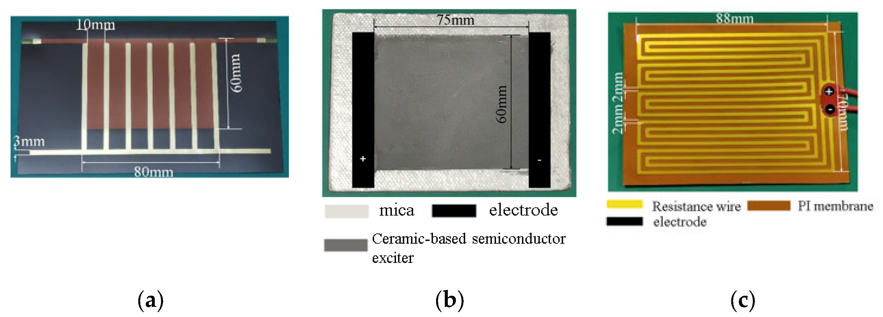
Three types of actuators—a comb-shaped plasma actuator, a ceramic-based semiconductor actuator [54,55,56], and a resistance wire actuator [57]—were meticulously examined and designed, as depicted in Figure 2. The plasma actuator is illustrated in Figure 2a, featuring high-voltage electrodes, insulating media, and low-voltage electrodes crafted from copper foil positioned above and below the insulating dielectric layer in a staggered arrangement. The high-voltage electrode copper foil has a width of 3 mm, while the low-voltage electrode copper foil is 10 mm wide, with a uniform thickness of 0.06 mm. The insulating dielectric layer made of polyimide (Kapton) tape has a thickness of 0.18 mm, and the discharge region measures 80 mm in length and 60 mm in width. Figure 2b showcases a ceramic-based semiconductor actuator composed of a ceramic-based semiconductor element and stacked mica material. In Figure 2c, a resistance wire actuator is displayed, constructed using a blend of resistance wire and polyimide (Kapton). The heating region of the resistance wire actuator employed in the experiment spans 88 mm in length and 70 mm in width, with a coated area measuring 75 mm in length and 60 mm in width. The thickness of all three materials falls within the micrometer range and is approximately equivalent.
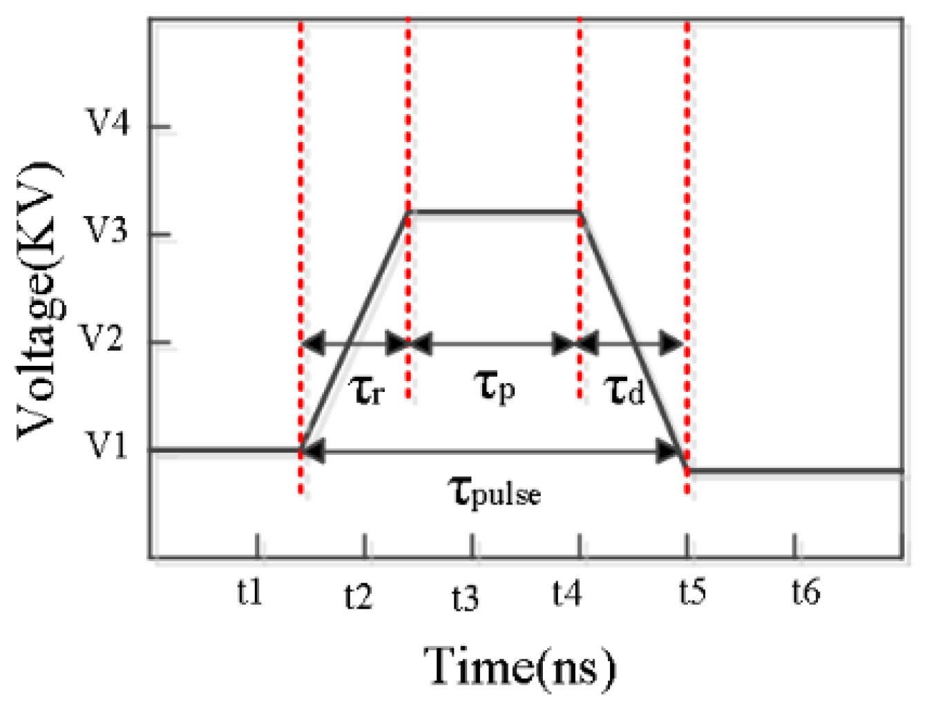
The power supply for the plasma actuator is a nanosecond pulse plasma excitation unit, and its voltage waveform is illustrated in Figure 3. This power supply offers adjustable output voltage ranges and pulse repetition frequencies, enabling precise control over pulse width and timing parameters. The peak range of the power output voltage is continuously adjustable from 0 to 20 kV. The pulse repetition frequency is continuously adjustable in the range of 1 Hz–20 kHz. The pulse width τP, rising edge time τR, and falling edge time τD can be adjusted. The adjustable range of the pulse width is 0 ns to 1 ms, and within this range, the pulse width is the middle section with relatively stable waveform changes. In contrast, the power supplies for resistance wire actuators and ceramic-based semiconductor actuators are stabilized DC sources with adjustable voltage and current ranges to suit the experimental requirements. The voltage adjustable range of this power supply is 0–30 V, and the current adjustable range is 0–30 A.

2.3. Ice-Making System

The experiment entailed the development of a specialized ice-making mold, a custom rectangular container fabricated from silicone. The mold exhibited a 5 mm wall thickness and internal dimensions measuring 160 mm in length, 60 mm in width, and 20 mm in height. The thickness of all three materials utilized in the mold fell within the micrometer range and maintained uniformity across them. Consequently, the material thickness was considered negligible during the ice-making process. To generate a 3 mm ice layer, three materials were affixed to the base of the ice-making container, and precise control over water injection volumes was crucial. To minimize potential errors arising from human involvement, standard large-range syringes and small-range pipettes were employed for water injection. The small-range pipette had a volume of 5 mL, ensuring minimal liquid extraction discrepancies. Figure 4 provides a visual representation of ice formation on the surface of various actuators.
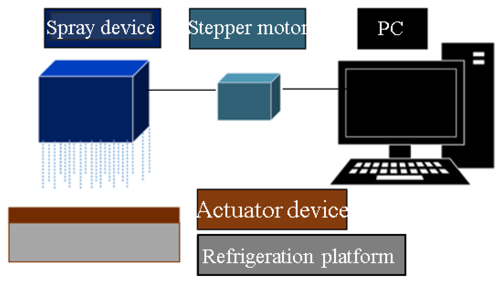
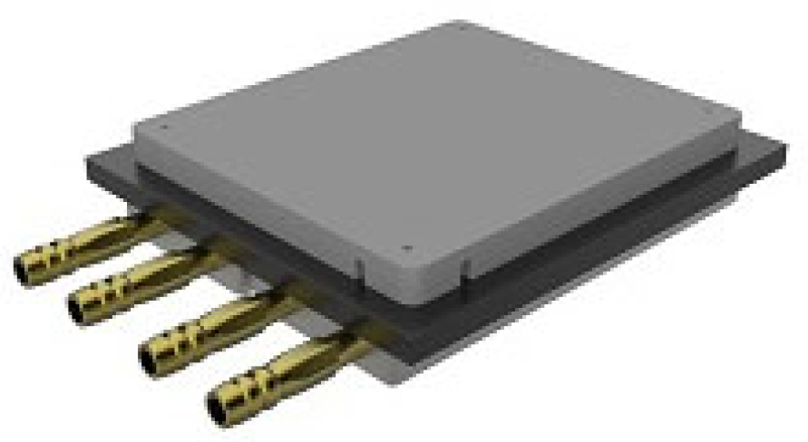
In real aircraft flight scenarios, ice accumulates layer by layer due to the impact of supercooled water droplets on aircraft surfaces, rather than forming a uniform ice layer instantaneously. To simulate this phenomenon, an experimental water-spray ice-making system was devised. This system, as depicted in Figure 5, comprised a spray mechanism and a semiconductor refrigeration platform. The spray system, controlled via a PC terminal, consisted of a spray apparatus, a stepper motor, and a computer interface for regulating the spray amount and intervals. The volume of each spray event was controlled by the stepper motor. In this study, the spray nozzle area measured 160 mm by 60 mm, with a nozzle outlet size of 0.1 mm. The spray device operated for 5 s per cycle, with a 10 s interval between sprays. Spraying ceased after reaching a total volume of 31.4 mL. Figure 6 illustrates a water-cooled semiconductor refrigeration platform leveraging semiconductor properties to induce refrigeration through current flow, i.e., the cold environment is maintained using an ice water machine or flowing water. The experiment utilized a DL-130-150 ultra-low-temperature refrigeration platform, capable of cooling within the range of −30 °C to −20 °C at ambient temperature. The refrigeration platform’s surface area spanned 250 mm in length and 250 mm in width, with temperature adjustments facilitated through the temperature control system. Figure 7 showcases the physical manifestation of the ice layer achieved through plasma spray ice-making.

3. Results

3.1. Typical Power Density Selection

To compare the effectiveness of three de-icing methodologies under identical power densities, power density evaluations were executed utilizing the actuator elaborated in Section 2.2. The power density calculation formula for the resistance wire and ceramic-based semiconductor actuators is delineated as follows:
p = UI S
In this equation, p signifies the power density, U symbolizes the DC source voltage, I denotes the DC source current, and S represents the heating area.
For the resistance wire actuator, the applied voltage varied between 5 V and 22 V at 0.5 V intervals, resulting in a power density spectrum spanning from 0.196 W/cm2 to 1.718 W/cm2. Conversely, the ceramic-based semiconductor actuator functioned within voltage parameters of 10 V to 26 V, measured at 1 V increments, yielding power densities ranging from 0.097 W/cm2 to 1.444 W/cm2.
The determination of power density for plasma actuators involved an integrative approach:
p = f · 0 T 0 u ( t ) i ( t ) d t S
In this context, p symbolizes the power density, and the denominator in the formula entails the integration of voltage u and current i over a specified duration within a single cycle, signifying the power consumption by the plasma actuator during a cycle. The parameter S denotes the heating area of the plasma actuator.
The power density calculation for plasma actuators involved an integration method, with the experimental evaluation revealing an applied voltage range of 3 kV to 6 kV and a frequency range of 1 kHz to 10 kHz. To streamline data analysis, three typical operational states (6 kV, 1 kHz; 6 kV, 4 kHz; 6 kV, 10 kHz) were chosen. The corresponding power densities were determined as 0.170 W/cm2, 0.727 W/cm2, and 1.427 W/cm2, respectively. By correlating these power densities with the input voltages for the resistance wire and ceramic-based semiconductor actuators within their respective power density ranges, optimal power densities and electrical parameters were selected, as detailed in Table 1.
The computation of power density for plasma actuators entailed an integrated method, with experimental scrutiny disclosing an applied voltage span of 3 kV to 6 kV and a frequency range of 1 kHz to 10 kHz. To facilitate data analysis, three distinct operational states (6 kV, 1 kHz; 6 kV, 4 kHz; 6 kV, 10 kHz) were selected. The corresponding power densities were identified as 0.170 W/cm2, 0.727 W/cm2, and 1.427 W/cm2, respectively. By establishing correlations between these power densities and the input voltages for the resistance wire and ceramic-based semiconductor actuators within their respective power density brackets, optimal power densities and electrical parameters were discerned, as outlined in Table 1.

3.2. Research on the De-Icing Performance of the Actuator

3.2.1. Research on the Thermal Characteristics and Static De-Icing Characteristics of Plasma Actuators at Room Temperature

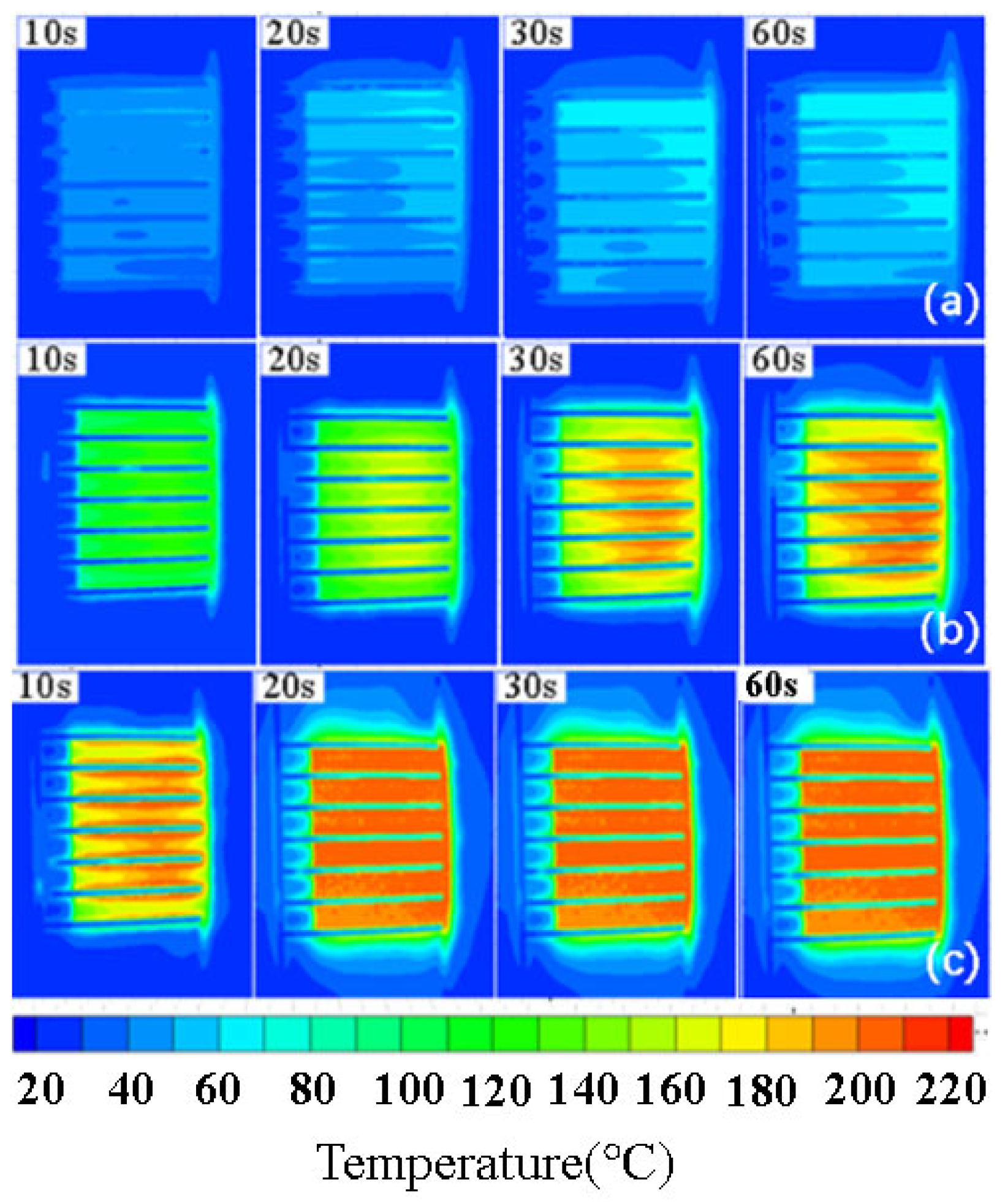
Figure 8 illustrates the infrared thermal image cloud map depicting the plasma actuator at varying power densities. Notably, the high-temperature region initially emerges near the high-voltage electrode due to the more intense plasma excitation discharge and higher heat in its vicinity. The area between the two electrodes experiences the weakest discharge, leading to a scenario where the temperature near the electrode surpasses that between the electrodes during the temperature elevation process. With increasing power density, the surface thermal equilibrium temperature of the plasma actuator rises, accompanied by a reduction in the time required to reach thermal equilibrium. Once thermal equilibrium is reached, the surface temperature distribution becomes uniform, with no noticeable low-temperature regions.
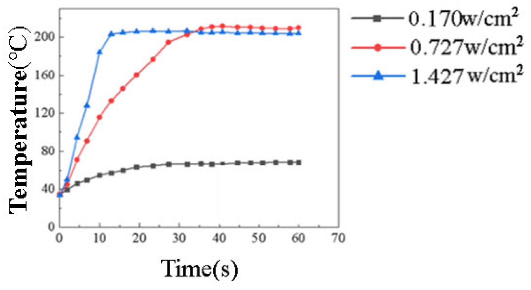
As shown in Figure 9, the temperature rise rate of the plasma actuator demonstrates a gradual decline across various power densities. At a power density of 0.170 W/cm2, the actuator achieves a thermal equilibrium temperature of 51.4 °C within 27 s, with the fastest temperature rise rate reaching 1.904 °C/s. With the power density escalating to 0.727 W/cm2, the actuator reaches a thermal equilibrium temperature of 203.7 °C in 83 s, characterized by a peak temperature rise rate of 2.454 °C/s. Similarly, at a power density of 1.427 W/cm2, the actuator attains a thermal equilibrium temperature of 201.3 °C within 58 s, with the swiftest temperature rise rate peaking at 3.471 °C/s. The trend indicates that higher power densities result in accelerated temperature rise rates and a quicker attainment of thermal equilibrium. However, as power density increases, the coupling between the power supply and the actuator weakens, leading to the thermal equilibrium temperature stabilizing rather than consistently rising.
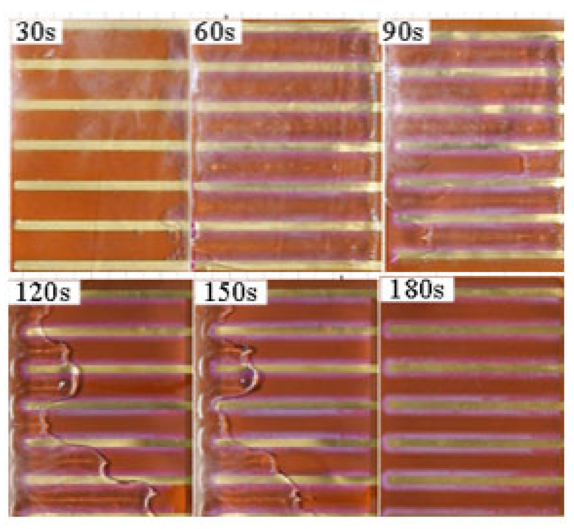
Figure 10 demonstrates the dynamic de-icing process when frozen ice is present on the surface of the plasma actuator. Initially, within the first thirty seconds of de-icing, the plasma actuator’s surface is covered in a thick layer of ice, impeding plasma production. Consequently, de-icing at this stage primarily relies on heat transfer from the actuator’s intermediate layer. As the dielectric layer continues to warm, the ice near the actuator’s surface transitions into water. The lower density of ice compared to water facilitates this transformation, allowing the actuator’s surface to interact with the surrounding air, enabling plasma generation. The thermal properties of plasma expedite ice melting. Subsequently, the ice layer gradually melts away from the side adjacent to the actuator. Through extended de-icing, the plasma actuator’s surface eventually comes into full contact with the ambient air. By 180 s, the complete elimination of ice accumulation from the actuator’s surface is achieved.
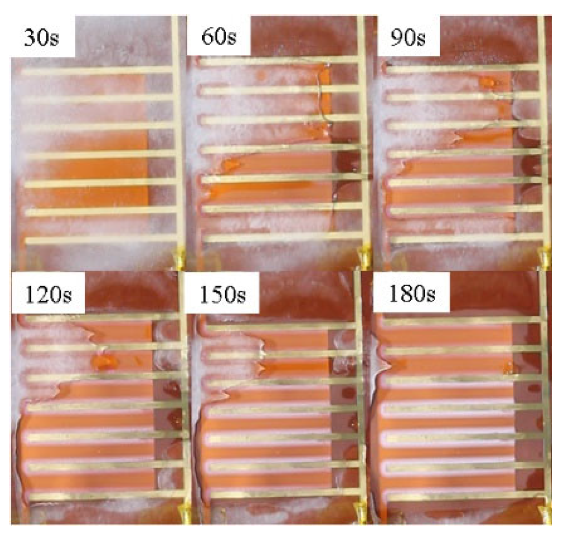
Figure 11 illustrates a power density of 0.727 W/cm2 within the plasma actuator during the de-icing process of the plasma actuator under water-spray icing conditions. The ice layer observed under these conditions presents a milky white appearance, resembling the frosted ice encountered in actual flight tests. Throughout the dynamic de-icing process, it becomes apparent that the presence of non-dense frost and ice results in significant air pockets within the ice layer. Consequently, during the initial stages of de-icing, favorable conditions emerge for the plasma actuator’s surface to generate plasma. Consequently, in comparison to frozen conditions, the de-icing area is more extensive simultaneously. Moreover, under identical power density levels, frosted ice proves to be more easily removed than clear ice.

3.2.2. Research on Room Temperature Thermal Characteristics and Static De-Icing Characteristics of Ceramic-Based Semiconductor Actuators

Figure 12 presents an infrared thermal image cloud map illustrating a ceramic-based semiconductor actuator under varying power densities. The graph reveals a swift surge in the surface temperature of the actuator upon power activation. Prior to reaching thermal equilibrium, the temperature distribution within the material displays higher values centrally and lower values peripherally, indicative of heat transfer dynamics resulting from contact with the surrounding environment. With increasing power densities, the material’s thermal equilibrium temperature rises, while the time required to reach thermal equilibrium decreases. At a power density of 0.170 W/cm2, the ceramic-based semiconductor actuator achieves thermal equilibrium after 60 s of heating, with the maximum equilibrium temperature remaining below 100 °C, and an uneven temperature distribution. Notably, the highest temperature region is concentrated in the center of the actuator, demonstrating a decreasing temperature gradient towards the periphery. In contrast, at a power density of 1.427 W/cm2, the time to reach thermal equilibrium can be reduced to 20 s, with the equilibrium temperature stabilizing around 210 °C and exhibiting a uniform distribution.
Figure 13 outlines the temperature rise curve of a ceramic-based semiconductor actuator under various power density excitation conditions in the absence of ice. Throughout the temperature rise process, the actuator exhibits a gradual decrease in the temperature rise rate. For instance, at a power density of 0.170 W/cm2, the actuator reaches a thermal equilibrium temperature of 63.7 °C after 36 s of heating, with an average maximum temperature rise rate of 1.769 °C/s. As the power density increases to 0.727 W/cm2 and 1.427 W/cm2, the actuator achieves thermal equilibrium temperatures of 210.7 °C and 208.3 °C in 41 s and 13 s, respectively, with the fastest temperature rise rates peaking at 5.139 °C/s and 16.023 °C/s. This trend underscores a pronounced nonlinear increase in the fastest temperature rise rate with rising power densities for ceramic-based semiconductor actuators.
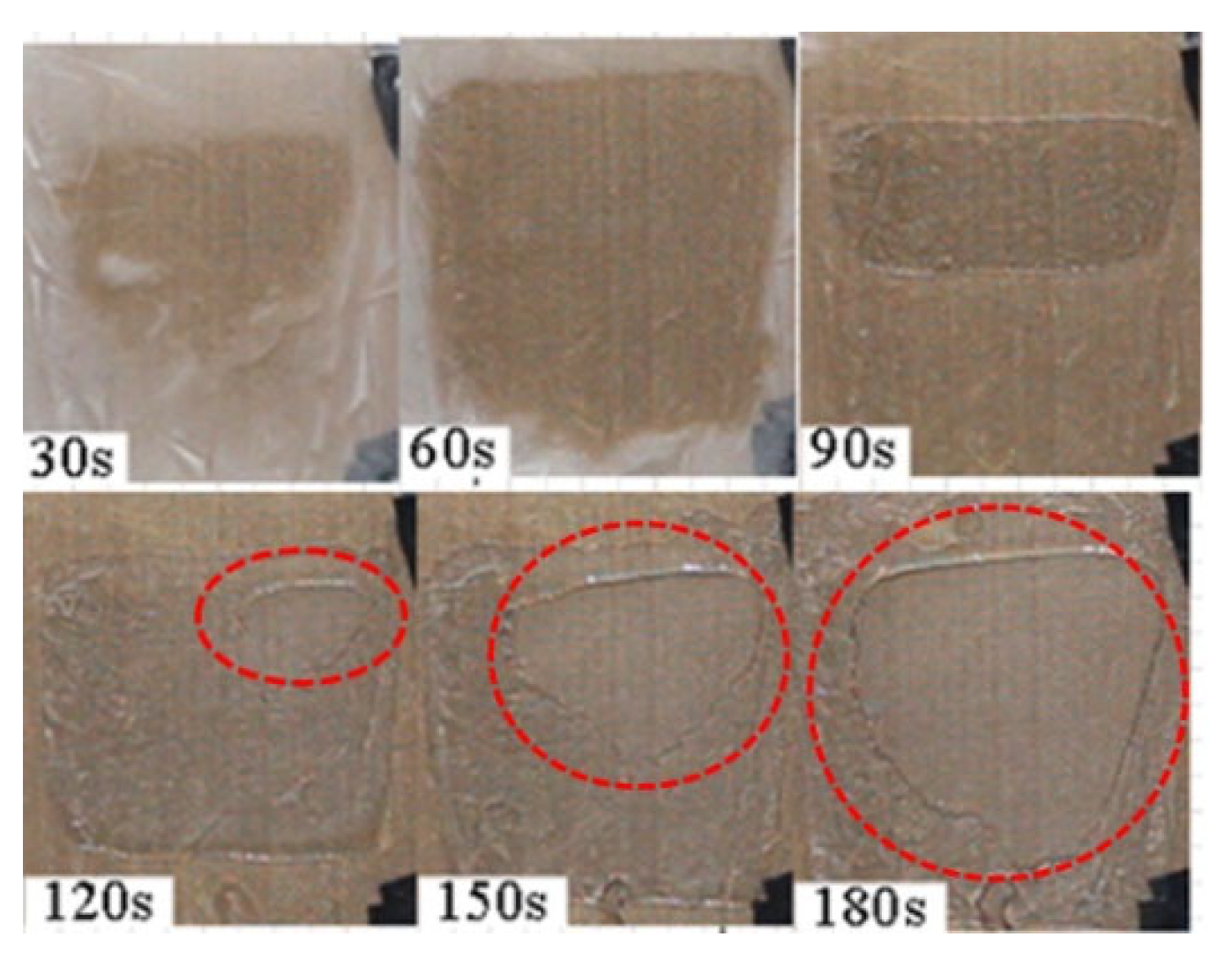
In Figure 14, the de-icing process of a ceramic-based semiconductor actuator under icy conditions at a power density of 0.727 W/cm2 is depicted. Upon activation, the actuator initiates the melting of the ice layer on its surface. The melted ice transforms into water and air, with the latter ascending due to density disparities. As the surface temperature of the actuator continues to rise, more ice transitions to water, forming an ice shell encapsulating water and air. Due to the lower thermal conductivity of air compared to water, a small aperture forms at the interface between the upper layer of the ice shell and the water. Subsequently, the water and air within the enclosure flow out through the aperture, causing it to expand progressively. This process persists as the heating duration increases, leading to continuous expansion until the entire ice shell is liquefied.

3.2.3. Research on Room Temperature Thermal Characteristics and Static De-Icing Characteristics of Resistance Wire Actuators

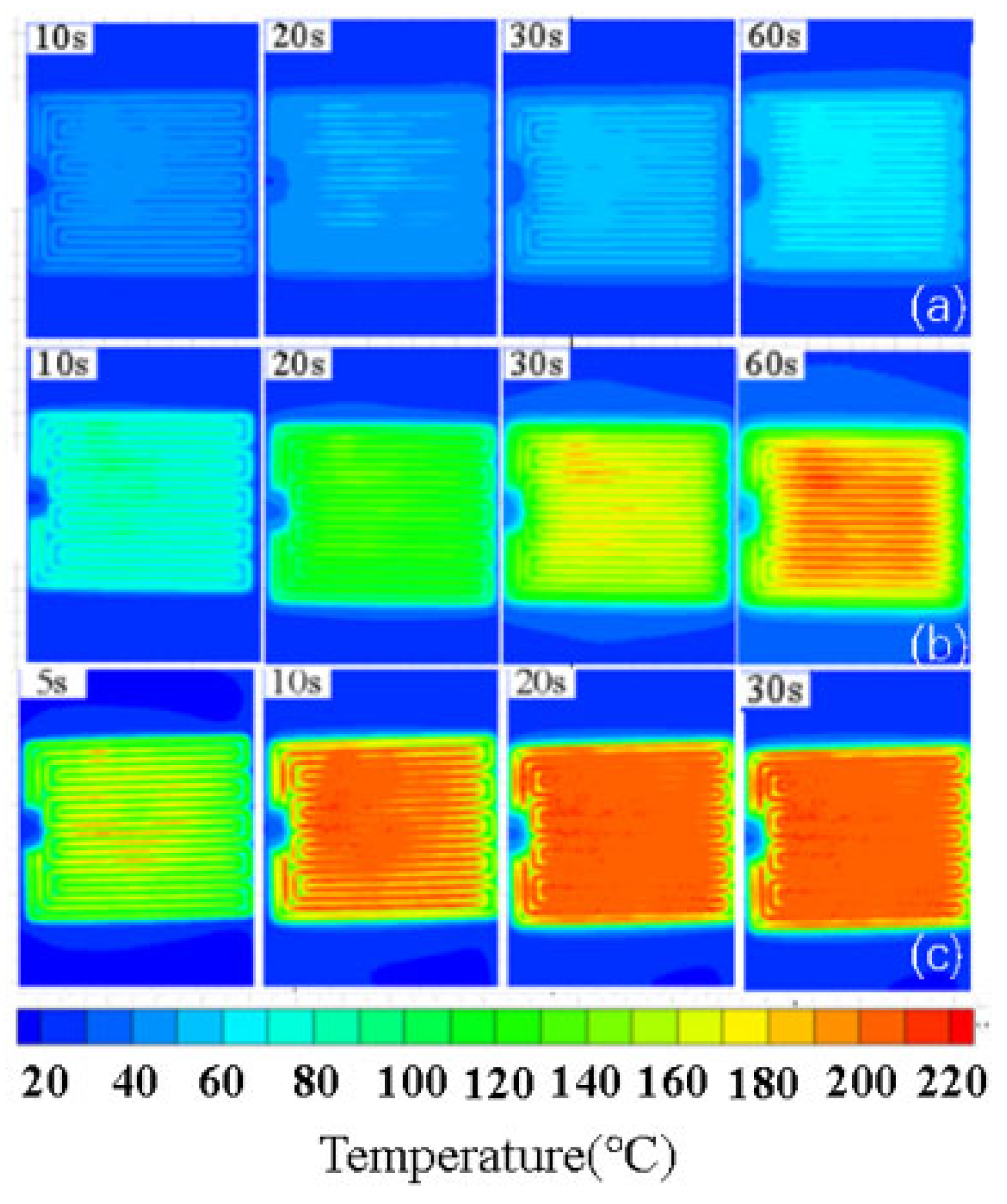
Figure 15 presents the infrared thermal imaging of a resistance wire actuator under varying power densities. The image showcases distinctive heating patterns exhibited by the resistance wire actuator in comparison to the ceramic-based semiconductor and plasma actuators. The heat distribution within the high-temperature region is intricately related to the arrangement of internal resistance wires. Upon circuit activation, heat generation commences within the resistance wire, whereas the plasma actuator triggers plasma formation and heat release by ionizing air through a high-voltage electrode. In contrast, the resistance wire actuator dissipates heat energy to the surrounding ambient air via thermal exchange, resulting in a slower temperature transfer rate. Consequently, temperatures are lower around the gap and diminish further away from the resistance wire. Notably, even upon reaching thermal equilibrium, a distinct cooler region persists between the two resistance wires.
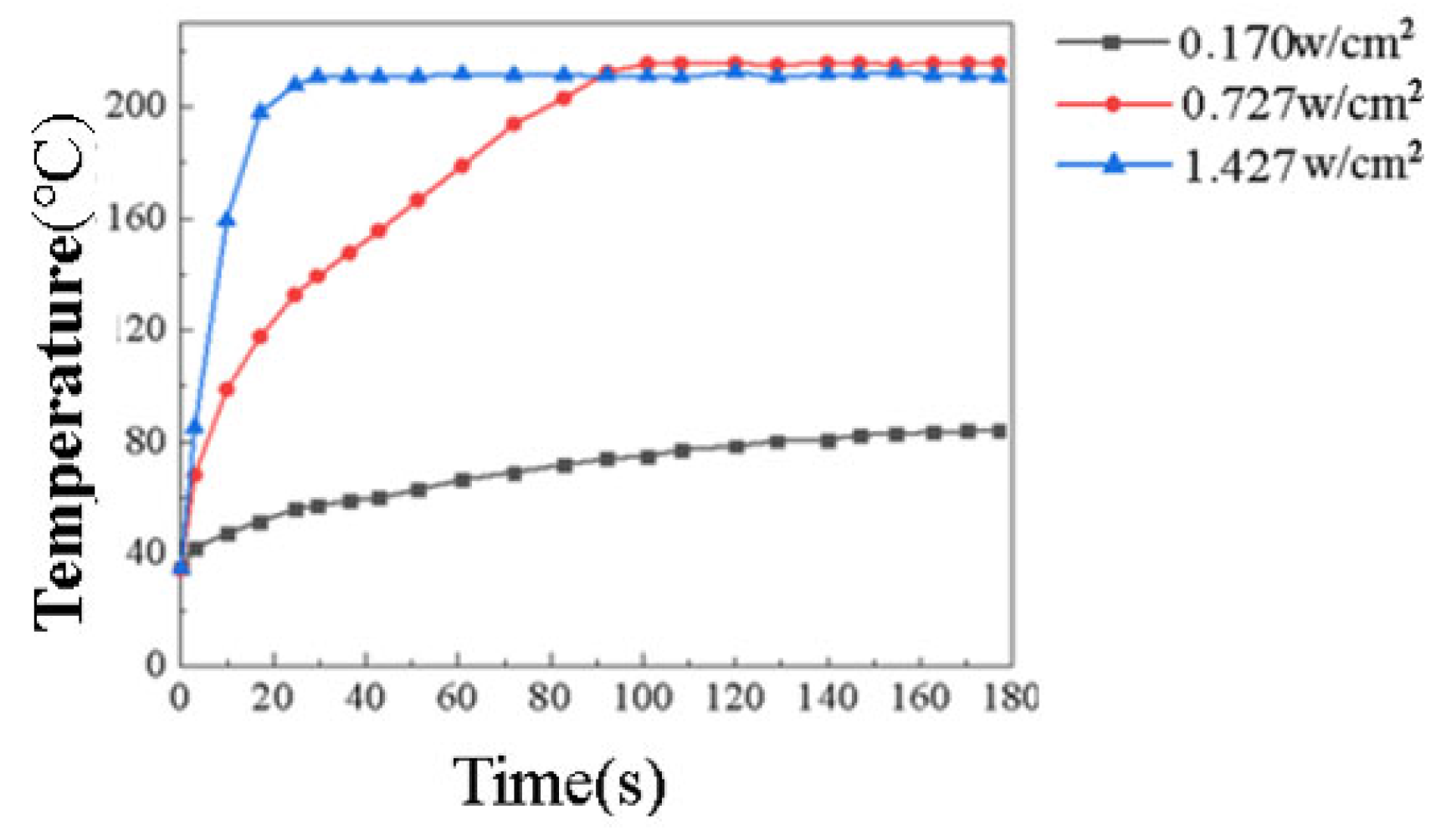
For an in-depth examination of the actuator’s heating dynamics, see Figure 16, which illustrates the fastest temperature rise curve of the resistance wire actuator under varied power densities in ice-free conditions. The graph demonstrates a gradual decrease in the temperature rise rate of the resistance wire actuator throughout the heating process. At a power density of 0.170 W/cm2, the actuator attains a thermal equilibrium temperature of 83.1 °C in 167 s, with a temperature rise rate of 1.001 °C/s. With a power density of 0.727 W/cm2, the actuator reaches a thermal equilibrium temperature of 210.7 °C in 102 s, displaying a fastest temperature rise rate of 2.066 °C/s. Upon increasing the power density to 1.427 W/cm2, the actuator achieves a thermal equilibrium temperature of 208.4 °C in 29 s, with the fastest temperature rise rate peaking at 7.186 °C/s. This trend highlights a nonlinear escalation in the fastest temperature rise rate of the resistance wire actuator as power densities increase.
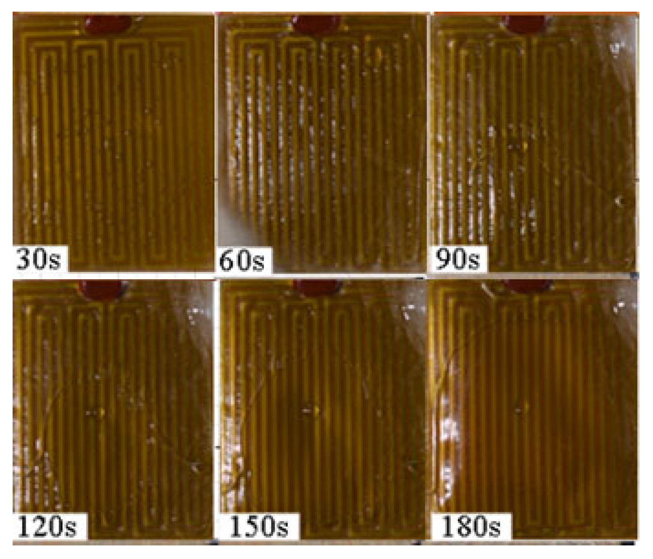
Figure 17 showcases the de-icing process of the resistance wire actuator under icy conditions at a power density of 0.727 W/cm2. The infrared thermal image captured at room temperature reveals a strip-shaped high-temperature heating area within the resistance wire actuator. The configuration of the resistance wires corresponds to the heating region, with the space between the two resistance wires delineating a relatively cooler zone. During the ice heating process, ice initially melts within the high-temperature region, forming water pathways. Subsequent heating leads to the melting of the surrounding ice layer, resulting in grooves on the actuator’s surface. A substantial ice-free area emerges after 120 s, with the de-icing process completed within 180 s as the heating progresses.

3.3. Comparative Study of Room-Temperature Thermal Characteristics of Various Actuators

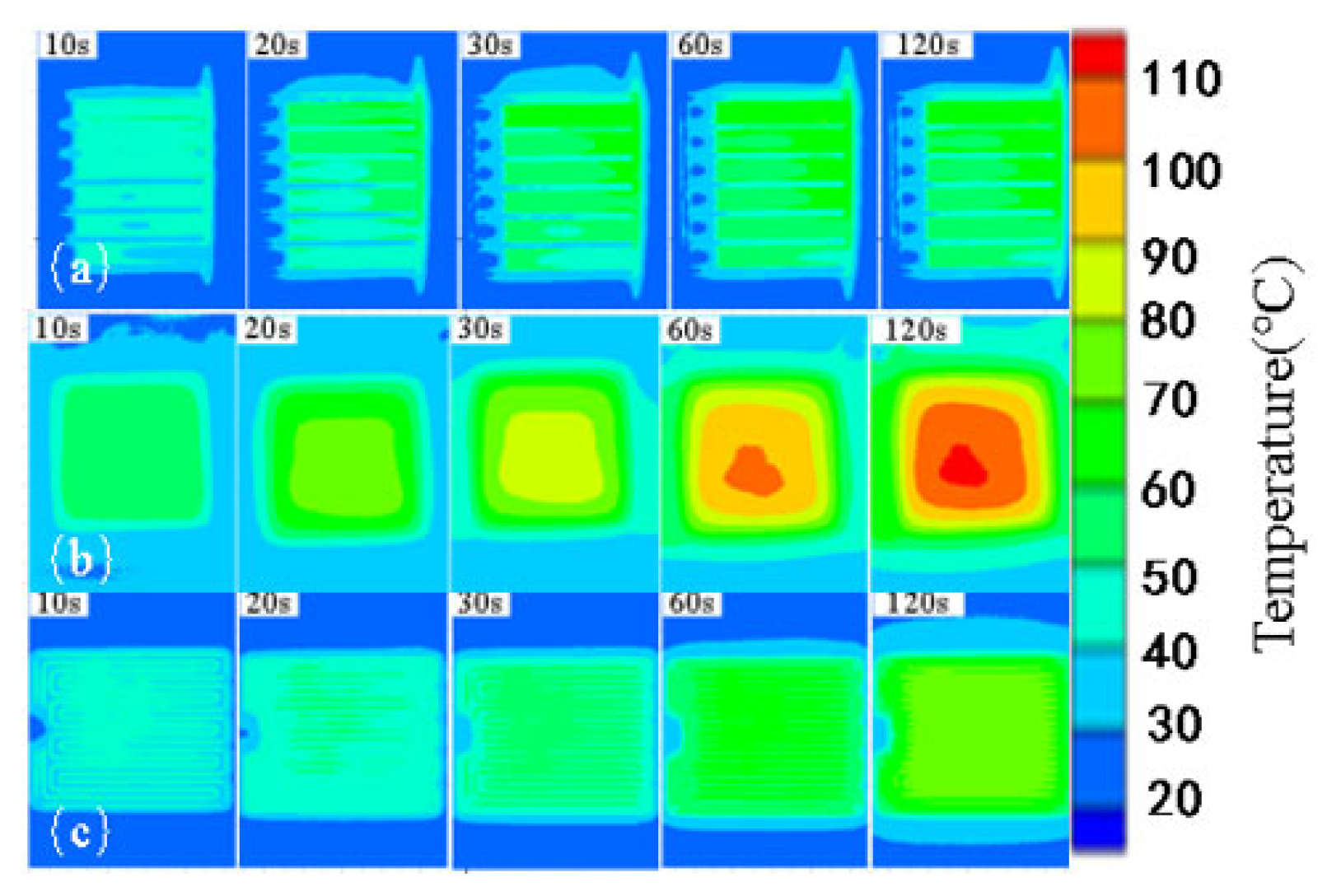
Figure 18 illustrates the infrared thermal cloud map of each actuator operating at a power density of 0.170 W/cm2. Under this power density condition, the ceramic-based semiconductor actuator demonstrates a significantly higher peak temperature than the plasma and resistance wire actuators after 30 s of heating. Subsequent observations at 60 s reveal a consistent rise in temperature on the surface of the ceramic-based semiconductor actuator. By the 120 s mark, the high-temperature region extends from the center towards the periphery. As the heating process advances, the temperature distribution across the resistance wire and plasma actuators becomes more uniform. Despite achieving thermal equilibrium after 30 s, the equilibrium temperature of the resistance wire actuator remains lower than that of the ceramic-based semiconductor actuator.
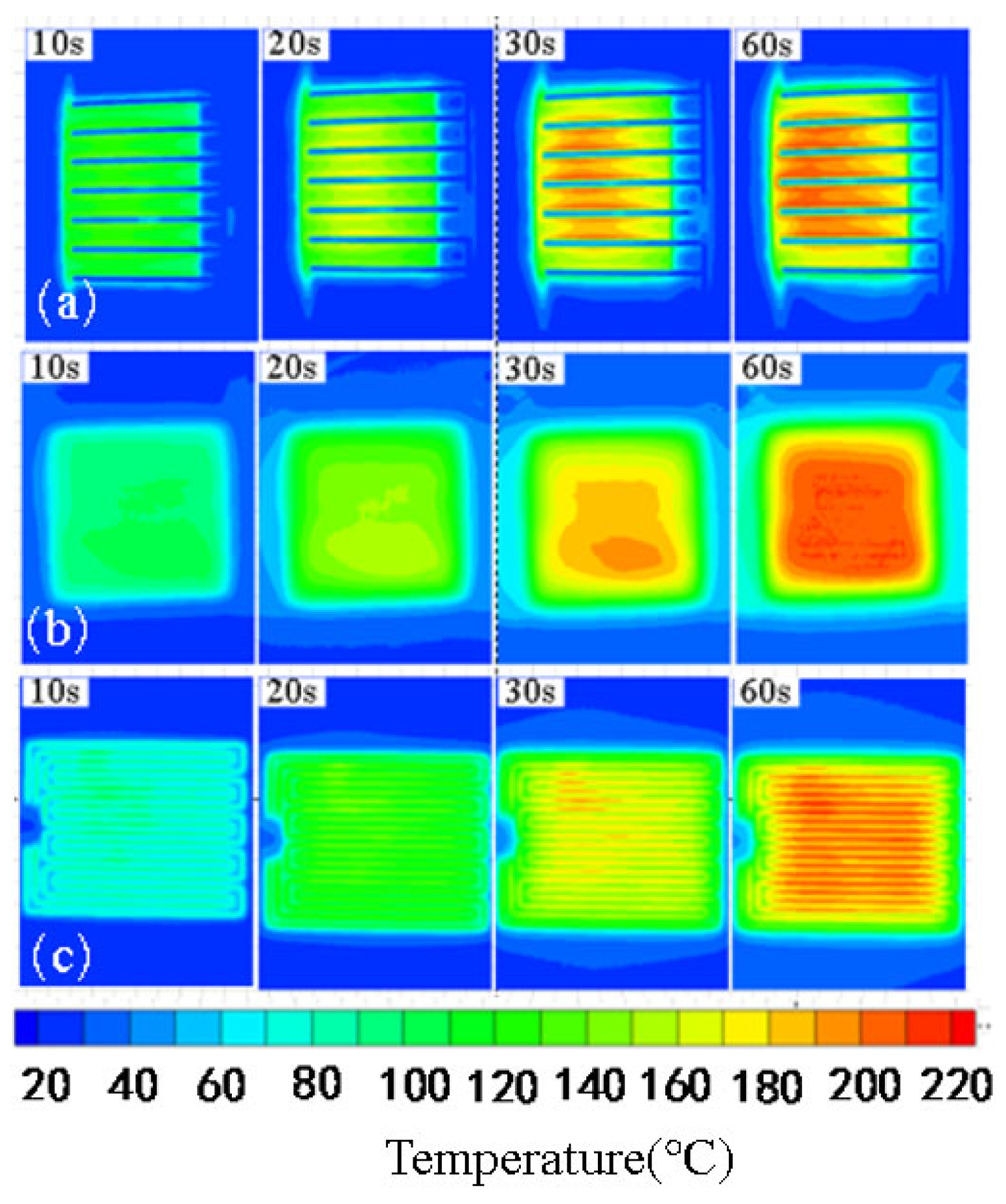
In Figure 19, the infrared thermal cloud map at a power density of 0.727 W/cm2 presents distinct temperature behaviors among the actuators. Initially, the plasma and ceramic-based semiconductor actuators exhibit higher average temperatures in the heating area compared to the resistance wire actuator after 10 s of heating. Subsequent time intervals of 20 and 30 s witness substantial temperature increases across all materials, with the plasma actuator showing a more pronounced rise and a larger heated area. By the 60 s mark, all three materials engage in stable heat exchange with the surrounding air, nearing thermal equilibrium. Notably, the temperature distribution among the actuators at around 210 °C becomes relatively uniform, with the ceramic-based semiconductor actuator displaying the broadest and most consistent distribution. The high-temperature area of the resistance wire actuator aligns with the locations of the resistance wires.
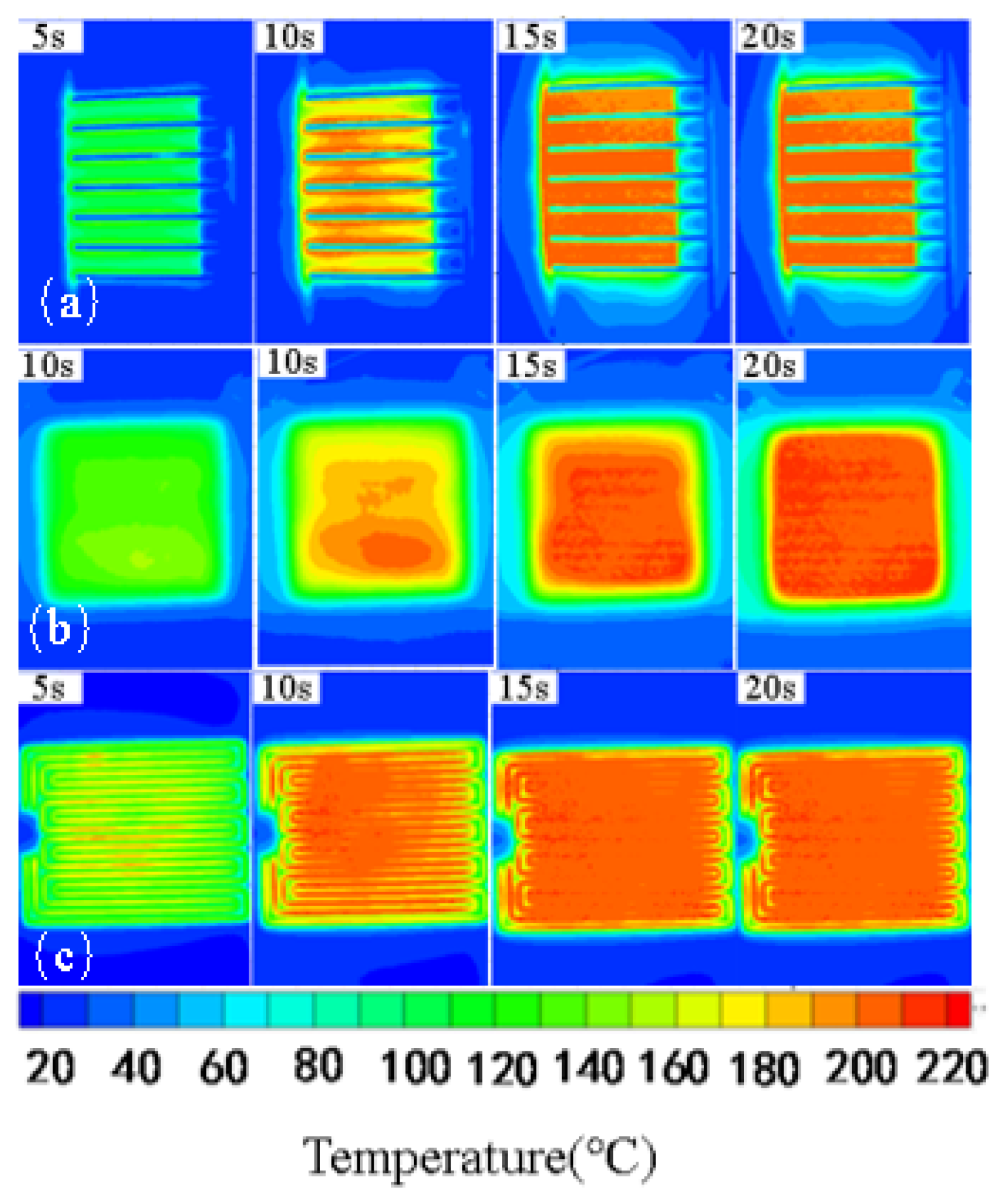
Figure 20’s infrared thermal cloud map at a power density of 1.427 W/cm2 reveals the temperature dynamics at different time intervals. After 5 s of heating, the resistance wire actuator achieves a significantly higher temperature than the plasma and ceramic-based semiconductor actuators, predominantly concentrated at the positions of the resistance wires. The plasma actuator shows the most uniform temperature distribution at this stage. Subsequent intervals demonstrate substantial temperature increases across all three materials. By 15 s, the ceramic-based semiconductor actuator exhibits improved temperature uniformity, aligning with the highest temperature regions out of all the materials. Both the resistance wire and plasma actuators reach thermal equilibrium by this point. At 20 s, the exchange of heat with the external environment results in a uniform temperature distribution across the heating area of the ceramic-based semiconductor actuator.
In Figure 21a, temperature rise curves for different materials at a power density of 0.170 W/cm2 are presented. All materials reach thermal equilibrium within 240 s, with the ceramic-based semiconductor, plasma, and resistance wire actuators stabilizing at 110 °C, 67 °C, and 90 °C, respectively. Notably, the plasma actuator exhibits rapid response times, with average temperature rise rates of 0.41 °C/s, 0.84 °C/s, and 1.38 °C/s for the resistance wire, plasma, and ceramic-based semiconductor actuators, respectively.
Figure 21b illustrates temperature rise curves at a power density of 0.727 W/cm2, where all materials achieve thermal equilibrium above 200 °C. The plasma actuator demonstrates a significantly higher temperature rise rate compared to the ceramic-based semiconductor and resistance wire actuators due to the convective heat transfer induced by plasma generation. After specific heating durations, thermal equilibrium temperatures are reached, with respective temperature rise rates of 6.30 °C/s, 4.45 °C/s, and 2.33 °C/s for the plasma, ceramic-based semiconductor, and resistance wire actuators.
Figure 21c showcases temperature rise curves at a power density of 1.427 W/cm2. The resistance wire actuator exhibits the highest temperature rise rate, reaching 213 °C after 6 s. The plasma actuator lags behind, reaching 201 °C after 11 s due to deteriorating coupling with increasing power density. The ceramic-based semiconductor actuator reaches 213.3 °C after 20 s. Notably, the resistance wire actuator demonstrates superior thermal characteristics at this power density. Comparisons of the slowest temperature rise point highlight the efficiency of the resistance wire actuator in reaching a thermal equilibrium temperature of 120 °C after 15 s, outperforming the ceramic-based semiconductor and plasma actuators.
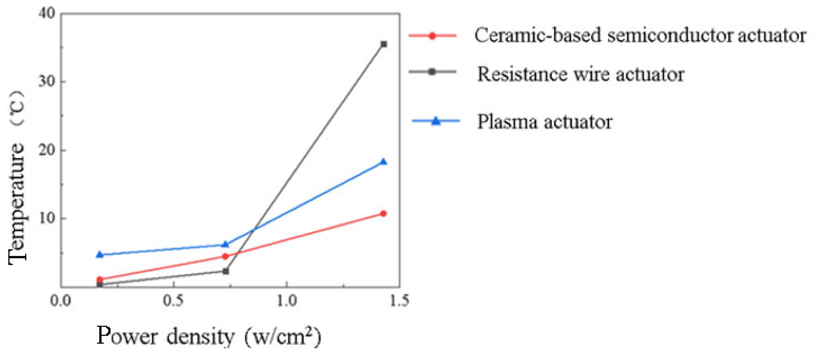
Figure 22 illustrates the temperature rise rates under varying power levels. A noticeable increase in temperature rise rate is observed as the power density escalates from 0.727 W/cm2 to 1.427 W/cm2. At the higher power density of 1.427 W/cm2, all three types of actuators exhibit significantly faster temperature rise rates compared to those at 0.727 W/cm2. Specifically, the relative increase in temperature rise rates is 68.482% for the plasma actuator, 67.927% for the ceramic-based semiconductor actuator, and 71.250% for the resistance wire actuator.
Observing the infrared thermal imaging images at different power densities, at a power density of 0.170 W/cm2, the ceramic-based semiconductor and plasma actuators exhibit faster temperature rise reactions than the resistance wire actuator. Additionally, the ceramic-based semiconductor actuator reaches the highest temperature, although its uniformity is inferior to that of the plasma actuator. At a power density of 0.727 W/cm2, the maximum heating equilibrium temperature of all three materials stabilizes around 210 °C. Notably, the time required to reach thermal equilibrium is significantly reduced, from 60 s to 20 s. With increasing power, the resistance wire actuators demonstrate a characteristic of rapid temperature rise. At a power density of 1.427 W/cm2, the temperature rise of the resistance wire actuator is notably swift with faster response times.

3.4. Comparison of De-Icing Characteristics of Various Materials under Ice Conditions

In practical de-icing processes, achieving effective de-icing while ensuring the efficient operation of each actuator at lower energy consumption is crucial. A comparison was conducted using the de-icing process diagram at a power density of 0.727 W/cm2.
Figure 23 illustrates the de-icing process of the three types of de-icing devices at various time points when frozen at −15 °C and operated at a power density of 0.727 W/cm2. Initially, the actuators’ surfaces are uniformly covered with ice. By 60 s of de-icing, an ice shell containing water and air forms on the actuator surface. At the 90 s mark, a small hole appears at the contact area between the upper layer of the ice shell and the water due to the lower thermal conductivity of air compared to water. Water and air trapped within the ice shell start flowing out through this hole, gradually expanding it. Throughout the de-icing process, both the resistance wire actuator and the plasma actuator exhibit strip-shaped heating areas; convective heat transfer and heat conduction represent the primary differences in heat transfer mechanisms between them.
During the 180 s de-icing process, the plasma actuator initially forms a cavity for de-icing. By 180 s, the de-icing process is nearly complete, extending gradually from the plasma generation area to cover the entire ice surface. Unlike the plasma actuator, the resistance wire actuator does not exhibit an ice shell structure during de-icing. However, a distinct ice band structure appears between 60 and 90 s of heating. After 120 s, the relative de-icing area of the resistance wire actuator is smaller than that of the plasma actuator, with de-icing extending from the area with resistance wire distribution to cover the entire surface. The de-icing process of the ceramic-based semiconductor actuator closely mirrors that of the plasma actuator.
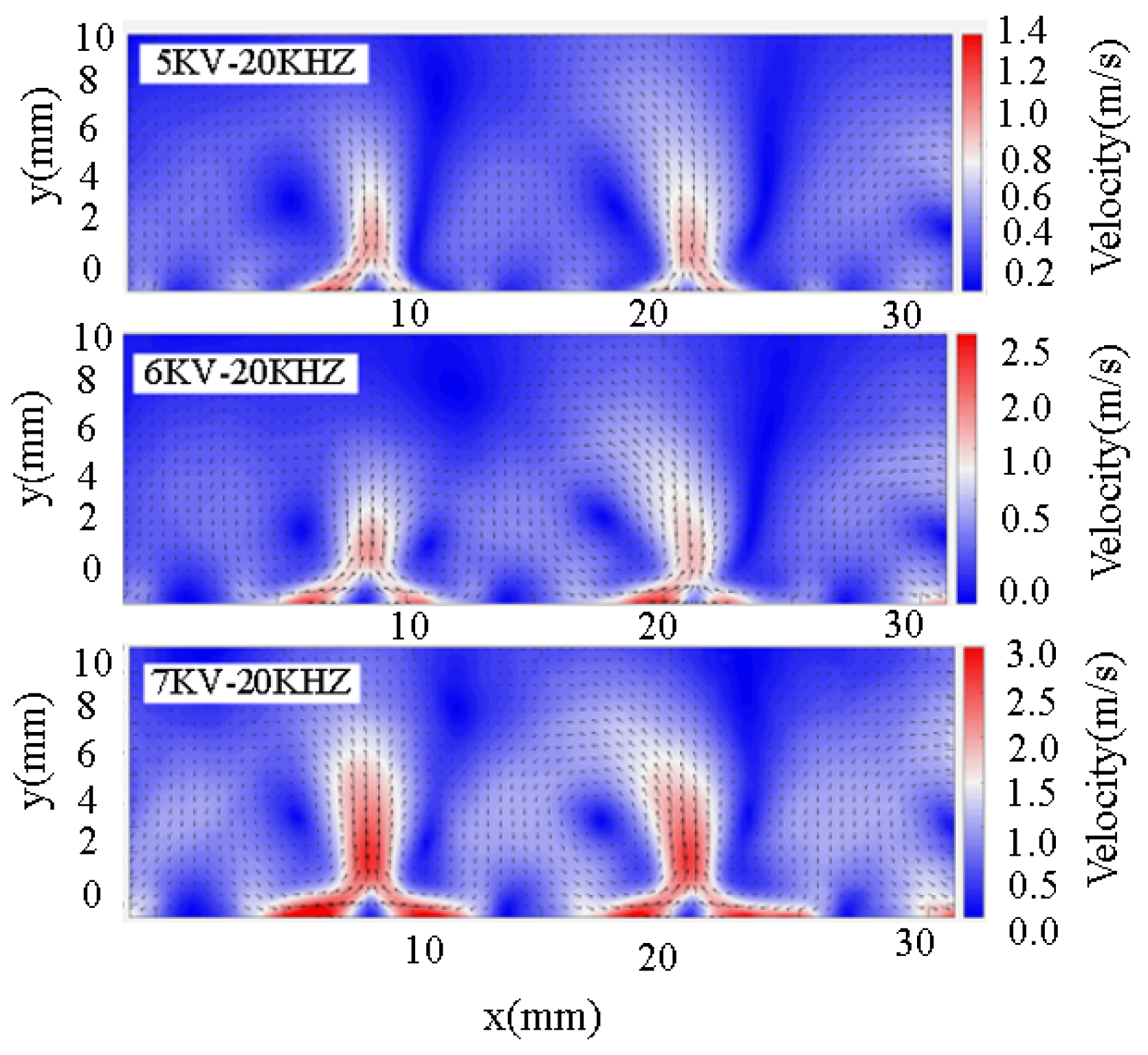
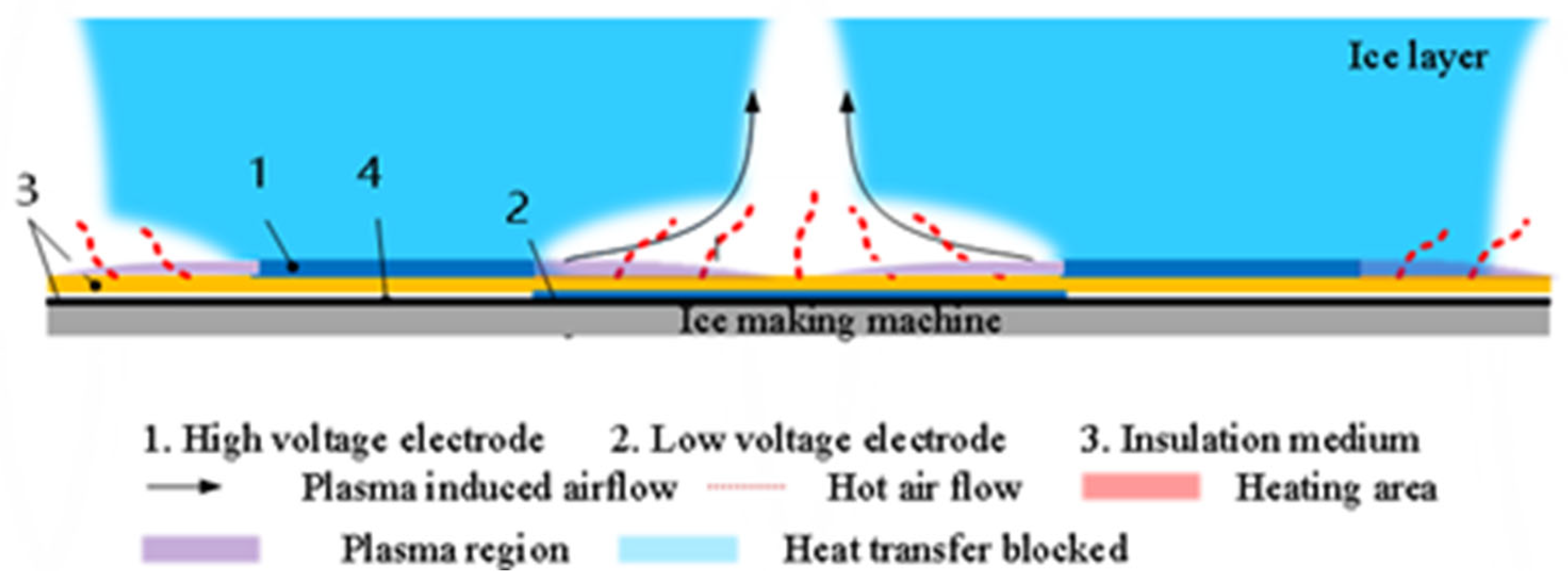
Figure 24 illustrates the flow field distribution of the plasma actuator under different applied voltages, showing an upward-induced airflow between the two positive electrodes. The heat transfer mode for the plasma actuator primarily involves convective heat transfer. Additionally, Figure 25 demonstrates that the heat generated by the plasma actuator originates from the discharge of air near the wall, effectively heating the actuator surface and the surrounding air.
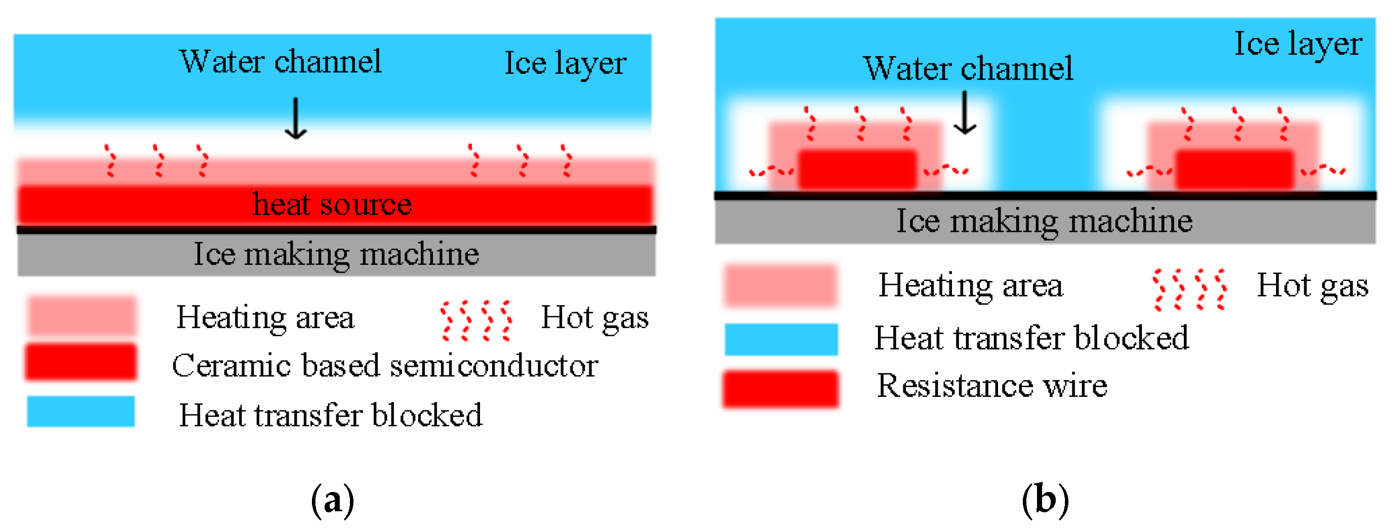
To elucidate the heat flow direction during de-icing, an analysis of the heat transfer mechanisms of plasma actuators, ceramic-based semiconductor actuators, and resistance wire actuators was conducted, as depicted in Figure 25 and Figure 26. The heat-generation methods differ among the actuators, with resistance wire actuators generating heat solely through the resistance wire, resulting in low heating efficiency in areas without the wire. In contrast, the entire ceramic-based semiconductor actuator serves as a heat source, resulting in uniform heat distribution without low-temperature regions.

4. Discussion

This study investigates the performance of three types of aircraft anti-icing and de-icing actuators under varying ice-free and icy conditions. The findings are as follows:
(1)
The analysis of the infrared thermal images of the three actuators across different power densities reveals that all can achieve thermal equilibrium temperatures exceeding 210 °C with increasing power density. The heating distribution of the plasma actuator is non-uniform, predominantly concentrated near the anode. In contrast, the resistance wire actuator displays distinct high- and low-temperature zones, leading to lower heat transfer efficiency. Conversely, the ceramic-based semiconductor actuator exhibits a gradual temperature decrease from the center to the circumference of the heating area. Once thermal equilibrium is reached, the high-temperature distribution becomes uniform across the entire heating area.
(2)
The comparison of the actuators’ temperature rise rates at various power densities shows that, at lower levels, ceramic-based semiconductor actuators and electric heating films exhibit faster temperature rise rates and reach thermal equilibrium temperatures. As power density increases, all three actuators ultimately attain the same thermal equilibrium temperature. However, higher power levels lead to a decreased thermal equilibrium temperature in the plasma actuator due to deteriorating coupling between the power supply and the actuator. Nonetheless, plasma actuators exhibit a faster temperature rise rate compared to ceramic-based semiconductor actuators and resistance wires. At lower power densities, ceramic-based semiconductor actuators demonstrate the quickest reaction time, while the resistance wire actuator achieves a notably higher surface temperature than the other two types. Conversely, at higher power densities, the resistance wire actuator surpasses the power density and thermal equilibrium temperature of the other two heating films.
(3)
The plasma-induced fluid flow on the actuator’s surface directs heat towards relatively cooler regions through convective heat transfer [58]. The heat transfer efficiency of the plasma actuator is notably lower than that of the resistance wire actuator due to its inherently static heat transfer nature. Consequently, the time taken for the plasma actuator’s lowest temperature rise point to reach thermal equilibrium is significantly shorter.

Author Contributions

J.Z. conducted experimental research; H.L. (Hua Liang) and B.W. supervised work and reviewed and edited manuscripts; D.B. provided resources for the experiment; J.Z. wrote the main manuscript; H.L. (Hongrui Liu) and S.L. analyzed the results. All authors have read and agreed to the published version of the manuscript.

Funding

This research was funded by Flight Safety Boundary Assessment and Application Research (No. 2A001101); High-level Science and Technology Innovation Talent Project Independent Research Project—Discipline Top Talents; and the National Natural Science Foundation of China (No: 52107174).

Data Availability Statement

The data and materials are available upon request.

Conflicts of Interest

The authors declare no conflicts of interest.

References

  1. Hu, M. The Harm of Ice Accumulation to Aircraft and Methods for Preventing and Removing Ice. Technol. Wind 2021, 5, 17–18. [Google Scholar]
  2. Xu, Z.; Su, Y.; Cao, Y. The influence and simulation of icing on aircraft maneuverability. J. Beijing Univ. Aeronaut. Astronaut. 2012, 38, 941–994. [Google Scholar]
  3. Yu, J.; Zhao, B.Y.; Bu, X.; Lin, G.; Li, Z. Numerical simulation of the performance of a certain aircraft engine nacelle hot air anti-icing system. Acta Aerodyn. Sin. 2016, 34, 302–307. [Google Scholar]
  4. Xu, J. Research on Electric Heating and Anti-Icing of Aircraft Windshield Glass. Master’s Thesis, Nanjing University of Aeronautics and Astronautics, Nanjing, China, 2012. [Google Scholar]
  5. Wei, Y.; Xu, H.; Xue, Y. The influence of wing leading edge icing on the operational stability characteristics of large aircraft. J. Beijing Univ. Aeronaut. Astronaut. 2017, 13, 56–58. [Google Scholar]
  6. Bourgault, Y.; Beaugendre, H.; Habashi, W.G. Development of a shallow-water icing model in FENSAP-ICE. J. Aircr. 2000, 37, 640–646. [Google Scholar] [CrossRef]
  7. Hedde, T.; Guffond, D. ONERA three-dimensional icing model. AIAA J. 1995, 33, 1038–1045. [Google Scholar] [CrossRef]
  8. Ferro, C.G.; Maggiore, P.; Champvillair, D. Development of a Computational Fluid Dynamics Model for Ice Formation: Validation and Parameter Analysis. Atmosphere 2023, 14, 834. [Google Scholar] [CrossRef]
  9. Gent, R.W. TRAJICE2—A Combined Water Droplet Trajectory and Ice Accretion Prediction Program for Aerofoils. RAE TR90054. 1990. Available online: https://ntrs.nasa.gov/api/citations/19970023937/downloads/19970023937.pdf (accessed on 24 March 2023).
  10. Wang, Z.; Jiang, H. Aircraft anti-icing system and its technological development status. China Sci. Technol. Inf. 2017, 13, 56–58. [Google Scholar]
  11. Li, B. Aircraft de-icing/anti-icing fluid and de-icing technology. Clean World 2012, 28, 26–31. [Google Scholar]
  12. Liu, C. Numerical Calculation and Experimental Research on Aircraft Electric Thermal Anti-Icing/De-Icing System. Master’s Thesis, Nanjing University of Aeronautics and Astronautics, Nanjing, China, 2021. [Google Scholar]
  13. Xiao, C. Research on Heat Transfer Characteristics and Effects of Aircraft Electric Deicing Process; China Aerodynamics Research and Development Center: Mianyang, China, 2011. [Google Scholar]
  14. Rekuviene, R.; Saeidiharzand, S.; Mažeika, L.; Samaitis, V.; Jankauskas, A.; Sadaghiani, A.K.; Gharib, G.; Muganlı, Z.; Koşar, A. A review on passive and active anti-icing and de-icing technologies. Appl. Therm. Eng. 2024, 250, 123474. [Google Scholar] [CrossRef]
  15. Li, L.; Liu, Y.; Tian, L.; Hu, H.; Hu, H.; Liu, X.; Hogate, I.; Kohli, A. An experimental study on a hot-air-based anti-/de-icing system for aero-engine inlet guide vanes. Appl. Therm. Eng. 2020, 167, 114778. [Google Scholar] [CrossRef]
  16. Pellissier MP, C.; Habashi, W.G.; Pueyo, A. Optimization via FENSAP-ICE of aircraft hot-air anti-icing systems. J. Aircr. 2011, 48, 265–276. [Google Scholar] [CrossRef]
  17. Li, H.; Zhou, M. Aircraft icing detection technology and engineering application of anti-icing and de-icing systems. Prog. Aviat. Eng. 2010, 1, 112–115. [Google Scholar]
  18. Wang, G.; Zhang, D.; Chen, H.; Chen, H.W. Aircraft Anti-Icing—Development from Traditional to Biomimetic. Ind. Technol. Innov. 2014, 1, 41–250. [Google Scholar]
  19. Shvydyuk, K.O. Long-lasting ceramic composites for surface dielectric barrier discharge plasma actuators. J. Eur. Ceram. Soc. 2023, 43, 6112–6121. [Google Scholar] [CrossRef]
  20. Liu, Y.; Xu, R.; Luo, N.; Liu, Y.; Wu, Y.; Yu, B.; Liu, S.; Zhou, F. All-Day Anti-Icing/De-Icing Coating by Solar-Thermal and Electric-Thermal Effects. Adv. Mater. Technol. 2021, 6, 2100371. [Google Scholar] [CrossRef]
  21. Pan, L.; Liu, Z.; Zhong, L.; Pang, X.; Wang, F.; Zhu, Y.; Ma, W.; Lv, Y. Carbon fiber/poly ether ether ketone composites modified with graphene for electro-thermal deicing applications. Compos. Sci. Technol. 2020, 192, 108–117. [Google Scholar] [CrossRef]
  22. Huang, J.; Li, D.; Peng, Z.; Zhang, B.; Yao, Y.; Chen, S. High-Efficient Anti-Icing/Deicing Method Based on Graphene Foams. ACS Appl. Mater. Interfaces 2023, 15, 43026–43037. [Google Scholar] [CrossRef] [PubMed]
  23. Khadak, A.; Subeshan, B.; Asmatulu, R. Studies on de-icing and anti-icing of carbon fiber-reinforced composites for aircraft surfaces using commercial multifunctional permanent superhydrophobic coatings. J. Mater. Sci. 2021, 56, 3078–3094. [Google Scholar] [CrossRef]
  24. Qin, W.; Lin, C.; Geng, J.; Xue, Y.; Zhong, M.; Zou, Y.; Liu, G. Multifunctional MXene/CNT-based layered film for icing detection, anti-icing, and deicing application. Ceram. Int. 2022, 48, 32767–32776. [Google Scholar] [CrossRef]
  25. Shvydyuk, K.O.; Nunes-Pereira, J.; Rodrigues, F.F.; Páscoa, J.C.; Lanceros-Mendez, S.; Silva, A.P. Holistic Characterization of MgO-Al2O3, MgO-CaZrO3, and Y2O3-ZrO2 Ceramic Composites for Aerospace Propulsion Systems. Ceramics 2024, 7, 364–384. [Google Scholar] [CrossRef]
  26. Tian, T. Theoretical and Experimental Research on Electric Heating Deicing of Graphene Composite Materials. Master’s Thesis, Nanjing University of Aeronautics and Astronautics, Nanjing, China, 2021. [Google Scholar]
  27. Shao, T.; Wang, R.; Zhang, C. Atmospheric-pressure pulsed discharges and plasmas: Mechanism, characteristics and applications. High Volt. 2018, 3, 14–20. [Google Scholar] [CrossRef]
  28. Chen, J.; Parsi, P.K.; Marklund, P.; Björling, M.; Shi, Y. Graphene-enhanced, wear-resistant, and thermal-conductive, anti-/de-icing gelcoat composite coating. Adv. Compos. Hybrid Mater. 2024, 7, 9. [Google Scholar] [CrossRef]
  29. Starikovskii, A.; Nikipelov, A.; Nudnova, M. SDBD plasma actuator with nanosecond pulse-periodic discharge. Plasma Sources Sci. Technol. 2009, 18, 34–35. [Google Scholar] [CrossRef]
  30. Tao, S.; Kaihua, L.; Cheng, Z. Experimental study on repetitive unipolar nanosecond-pulse dielectric barrier discharge in air at atmospheric pressure. J. Phys. D Appl. Phys. 2008, 41, 215203. [Google Scholar] [CrossRef]
  31. Erfani, R.; Zare-Behtash, H.; Kontis, K. Plasma actuator: Influence of dielectric surface temperature. Exp. Therm. Fluid Sci. 2012, 42, 258–264. [Google Scholar] [CrossRef]
  32. Khomich, V.Y.; Yamshchikov, V.A. Effect of power supply modes of multi-discharge actuator systems on their electric discharge and gas-dynamic characteristics. Acta Astronaut. 2024, 215, 135–141. [Google Scholar] [CrossRef]
  33. Barni, R.; Roman, H.E.; Riccardi, C. Ionizing Waves in Surface Dielectric Barrier Discharges Plasma Actuators. Actuators 2024, 13, 86. [Google Scholar] [CrossRef]
  34. Kuzenov, V.V.; Ryzhkov, S.V.; Varaksin, A.Y. Computational and Experimental Modeling in Magnetoplasma Aerodynamics and High-Speed Gas and Plasma Flows (A Review). Aerospace 2023, 10, 662. [Google Scholar] [CrossRef]
  35. Abdollahzadeh, M.; Rodrigues, F.; Nunes-Pereira, J.; Pascoa, J.C.; Pires, L. Parametric optimization of surface dielectric barrier discharge actuators for ice sensing application. Sens. Actuators A Phys. 2022, 335, 113391. [Google Scholar] [CrossRef]
  36. Zhang, J.; Liu, X.; Liang, H.; Xie, L.; Wei, B.; Zong, H.; Wu, Y.; Li, Y. Improving flight performance of UAVs by ice shape modulation. Chin. J. Aeronaut. 2024, in press. [Google Scholar] [CrossRef]
  37. Zhang, X.; Wang, X. Research progress and outlook of flow field created by dielectric barrier discharge plasma actuators driven by a sinusoidal alternating current high-voltage power. Chin. J. Theor. Appl. Mech. 2023, 55, 285–298. [Google Scholar]
  38. Sekimoto, S.; Fujii, K.; Anyoji, M.; Miyakawa, Y.; Ito, S.; Shimomura, S.; Nishida, H.; Nonomura, T.; Matsuno, T. Flow control around NACA0015 airfoil using a dielectric barrier discharge plasma actuator over a wide range of the Reynolds number. Actuators 2023, 12, 43. [Google Scholar] [CrossRef]
  39. Moayedi, H.; Amanifard, N.; Deylami, H.M. Parametric study of DBD plasma actuator for heat transfer enhancement in flow over a flat plate at low Reynolds numbers. J. Electrost. 2023, 124, 103825. [Google Scholar] [CrossRef]
  40. Shao, T.; Zhang, C.; Long, K. Surface modification of polyimide films using unipolar nanosecond-pulse DBD in atmospheric air. Appl. Surf. Sci. 2010, 256, 3888–3894. [Google Scholar] [CrossRef]
  41. Tian, M.; Song, H.; Liang, H. Experimental Study on Dielectric Barrier Discharge Plasma Anti-icing and Deicing. CIESC J. 2019, 70, 4247–4256. [Google Scholar]
  42. Zhang, X.; Yugang, Z.; Chun, Y. Recent developments in thermal characteristics of surface dielectric barrier discharge plasma actuators driven by sinusoidal high-voltage power. Chin. J. Aeronaut. 2023, 36, 1–21. [Google Scholar] [CrossRef]
  43. Zhong, Y.; Jin, Z.; Chen, M.; Yang, Z. An experimental investigation of the thermal effects in AC-DBD plasma actuator on the melting process of an ice bead. Exp. Therm. Fluid Sci. 2023, 147, 110950. [Google Scholar] [CrossRef]
  44. Chen, Z.; Wong, C.C.; Wen, C.Y. Thermal effects on the performance of a nanosecond dielectric barrier discharge plasma actuator at low air pressure. Phys. Fluids 2023, 35, 017110. [Google Scholar] [CrossRef]
  45. Benmoussa, A.; Belasri, A.; Harrache, Z. Numerical investigation of gas heating effect in dielectric barrier discharge for Ne-Xe exclam. Curr. Appl. Phys. 2017, 17, 479–483. [Google Scholar] [CrossRef]
  46. Tian, Y.; Cai, J.; Yang, L. Experimental study on thermal effects of pulsed dielectric barrier discharge plasma. J. Aerodyn. 2019, 34, 2663–2676. [Google Scholar]
  47. Meng, X.; Hui, W.; Yi, X. Current status and prospects of AC-SDBD plasma excitation anti-icing/deicing research. Acta Aerodyn. Sin. 2022, 40, 31–49. [Google Scholar]
  48. Chen, J.; Liang, H.; Li, Y. Experimental Study on Anti-Icing Performance of NS-DBD Plasma Actuator. Appl. Sci. 2018, 8, 1889. [Google Scholar] [CrossRef]
  49. Liu, X.; Liang, H.; Zong, H. NACA0012 airfoil plasma ice shape control experiment. Chin. J. Aeronaut. 2022, 43, 398–409. [Google Scholar]
  50. Chen, J.; Liang, H.; Jia, M. Experimental Study on Heat Transfer Process of Large Liquid Droplets Impacting on Ice Formation and Dielectric Barrier Discharge for Deicing. CIESC J. 2018, 69, 3825–3834. [Google Scholar]
  51. Liang, H.; Xie, L.; Wu, Y. Experimental study on plasma ice shape control to improve aerodynamic performance of airfoils/wings. Acta Aerodyn. Sin. 2021, 39, 156–164+195. [Google Scholar]
  52. Wei, B.; Wu, Y.; Liang, H. SDBD-based plasma anti-icing: A stream-wise plasma heat knife configuration and criteria energy analysis. Int. J. Heat Mass Transf. 2019, 138, 163–172. [Google Scholar] [CrossRef]
  53. Kolbakir, C.; Hu, H.; Liu, Y. An Experimental Investigation on the Thermodynamic Characteristics of DBD Plasma Actuations for Aircraft Icing Mitigation. Plasma Sci. Technol. 2022, 25. [Google Scholar]
  54. Tian, T.; Wang, Y.; Tao, M.; Zhu, C. Experimental Study on Electrothermal Deicing of Graphene Composite Materials. Sci. Technol. Eng. 2019, 19, 390–395. [Google Scholar]
  55. Rahimi, A.; Hojjati, M.; Dolatabadi, A.; Moreau, C. Thermal spray coating on polymeric composite for de-icing and anti-icing applications. J. Manuf. Sci. Eng. 2021, 143, 101008. [Google Scholar] [CrossRef]
  56. Zhang, L.; Gao, C.; Zhong, L.; Zhu, L.; Chen, H.; Hou, Y.; Zheng, Y. Robust photothermal superhydrophobic coatings with dual-size micro/nano structure enhance anti-/de-icing and chemical resistance properties. Chem. Eng. J. 2022, 446, 137461. [Google Scholar] [CrossRef]
  57. Zhao, Z.; Chen, H.; Liu, X. Development of highly efficient synthetic electric heating coating for anti-icing/de-icing. Surf. Coat. Technol. 2018, 349, 340–346. [Google Scholar] [CrossRef]
  58. Rodrigues, F.; Abdollahzadehsangroudi, M.; Nunes-Pereira, J.; Páscoa, J. Recent Developments on Dielectric Barrier Discharge (DBD) Plasma Actuators for Icing Mitigation. Actuators 2022, 12, 5. [Google Scholar] [CrossRef]
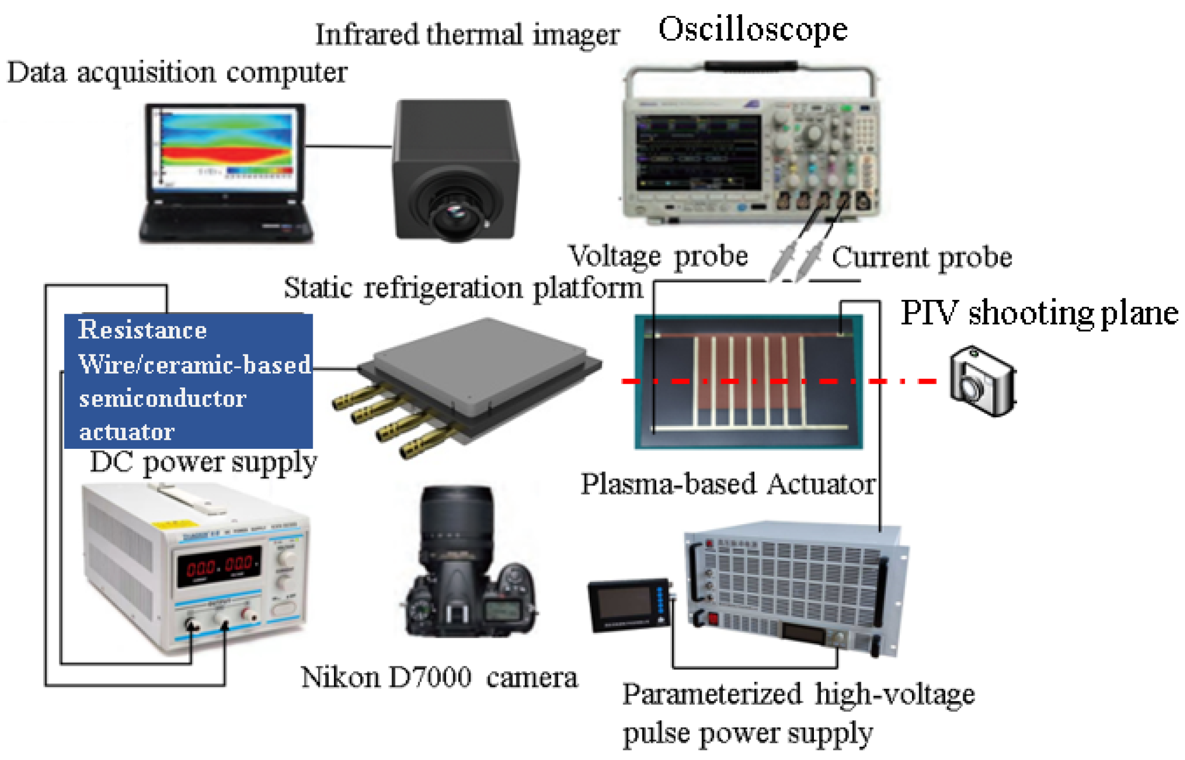
Figure 1. Measurement system.
Actuators 13 00226 g001
Figure 2. Physical picture of the actuator: (a) physical image of plasma actuator; (b) physical diagram of ceramic-based semiconductor actuator; (c) physical diagram of resistance wire actuator.
Actuators 13 00226 g002
Figure 3. Output voltage waveform of nanosecond pulse power supply.
Actuators 13 00226 g003
Figure 4. Physical picture of ice layer obtained by freezing method: (a) plasma actuator; (b) ceramic-based semiconductor actuator; The red dashed box in the figure represents the actual size and position of the actuator. (c) resistance wire actuator.
Actuators 13 00226 g004
Figure 5. The ice-making system with water-spray freezing.
Actuators 13 00226 g005
Figure 6. Physical picture of water-cooled semiconductor refrigeration platform.
Actuators 13 00226 g006
Figure 7. Physical picture of plasma actuator using water spray for ice-making.
Actuators 13 00226 g007
Figure 8. Infrared thermal images of the plasma actuator at all times under ice-free conditions: (a) 0.170 W/cm2; (b) 0.727 W/cm2; (c) 1.427 W/cm2.
Actuators 13 00226 g008
Figure 9. The fastest temperature rise curve of the plasma actuator under different power density conditions without ice. The selected power densities are 0.170 W/cm2, 0.727 W/cm2, and 1.427 W/cm2, respectively.
Actuators 13 00226 g009
Figure 10. Dynamic diagram of the de-icing process of plasma actuator under ice conditions at various times.
Actuators 13 00226 g010
Figure 11. Dynamic diagram of the de-icing process of plasma actuator under water-spraying conditions at various times.
Actuators 13 00226 g011
Figure 12. Infrared thermal images of ceramic-based semiconductor actuator at various times under ice-free conditions: (a) 0.170 W/cm2; (b) 0.727 W/cm2; (c) 1.427 W/cm2.
Actuators 13 00226 g012
Figure 13. Temperature rise curves of various power densities for ceramic-based semiconductor actuator under ice-free conditions.
Actuators 13 00226 g013
Figure 14. Dynamic diagram of the de-icing process of the ceramic-based semiconductor actuator under freezing conditions at different times. (The red dashed circle in the picture is used to facilitate readers to see the area of de-icing).
Actuators 13 00226 g014
Figure 15. Infrared thermal images of resistance wire actuators under ice-free conditions at all times: (a) 0.170 W/cm2; (b) 0.727 W/cm2; (c) 1.427 W/cm2.
Actuators 13 00226 g015
Figure 16. Temperature rise curve of resistance wire actuator under different power densities under ice-free conditions.
Actuators 13 00226 g016
Figure 17. De-icing process of resistance wire actuator at different moments under frozen ice conditions.
Actuators 13 00226 g017
Figure 18. Infrared thermal images of different actuators at different times at 0.170 w/cm2: (a) plasma actuator; (b) ceramic-based semiconductor actuator; (c) resistance wire actuator.
Actuators 13 00226 g018
Figure 19. Infrared thermal images of different actuators at different times at 0.727 W/cm2: (a) plasma actuator; (b) ceramic-based semiconductor actuator; (c) resistance wire actuator.
Actuators 13 00226 g019
Figure 20. Infrared thermal images of different actuators at different times at 1.427 W/cm2: (a) plasma actuator; (b) ceramic-based semiconductor actuator; (c) resistance wire actuator.
Actuators 13 00226 g020
Figure 21. The highest temperature rise curve of each actuator under different powers: (a) 0.170 W/cm2; (b) 0.727 W/cm2; (c) 1.427 W/cm2.
Actuators 13 00226 g021
Figure 22. The fastest temperature rise rate of each actuator under different power densities.
Actuators 13 00226 g022
Figure 23. De-icing process diagram of each actuator at different times with a power density of 0.727 w/cm2: (a) plasma actuator; (b) ceramic-based semiconductor actuator; (c) resistance wire actuator.
Actuators 13 00226 g023
Figure 24. Flow field analysis of plasma actuator.
Actuators 13 00226 g024
Figure 25. Heat transfer mechanism diagram of plasma actuator de-icing.
Actuators 13 00226 g025
Figure 26. Heat transfer mechanism diagram of different actuators: (a) resistance wire actuator; (b) ceramic-based semiconductor actuator.
Actuators 13 00226 g026
Table 1. Power selection of different actuators.
GroupPlasma ActuatorCeramic-Based
Semiconductor Actuator
Resistance Wire Actuator
16 kV 1 kHZ
0.170 W/cm2
11 V 0.7 A
0.171 W/cm2
6.5 V 1.6 A
0.169 W/cm2
26 kV 4 kHZ
0.727 W/cm2
20 V 1.7 A
0.756 W/cm2
14 V 3.2 A
0.727 W/cm2
36 kV 10 kHZ
1.427 W/cm2
26 V 2.5 A
1.444 W/cm2
20.5 V 4.4 A
1.464 W/cm2
Disclaimer/Publisher’s Note: The statements, opinions and data contained in all publications are solely those of the individual author(s) and contributor(s) and not of MDPI and/or the editor(s). MDPI and/or the editor(s) disclaim responsibility for any injury to people or property resulting from any ideas, methods, instructions or products referred to in the content.