Article

Downsizing Effects on Micro and Nano Comb Drives

1
Department of Information Engineering, Electronics and Telecommunications, University of Rome La Sapienza, 00184 Rome, Italy
2
Department of Industrial, Electronic and Mechanical Engineering, Roma Tre University, Via Della Vasca Navale 79, 00146 Rome, Italy
3
Institute of Photonics and Nanotechnologies, IFN-CNR, 00156 Rome, Italy
*
Author to whom correspondence should be addressed.
Actuators 2022, 11(3), 71; https://doi.org/10.3390/act11030071
Submission received: 25 January 2022 / Revised: 21 February 2022 / Accepted: 22 February 2022 / Published: 25 February 2022
(This article belongs to the Section Miniaturized and Micro Actuators)

Abstract

:
Downscaling has been a focal task of Electronics and Electromechanics in the last few decades, and a great engine for technological progress as well. Nevertheless, a scaling operation affects device physics, functioning and performance. The present paper investigates about the impact of scaling on a test case compliant electrostatic micro or nano actuator that is under development with two preferred micro fabrication methods, namely, thick SOI and thin amorphous silicon. A series of numerical trials on materials strength, electro-mechanical characteristics, sensitivity and overall actuation performance have been carried out at different grades of down-scaling and of aspect ratio. This gave rise to new design charts that we propose here as a predictive and friendly guide to select the most appropriate micro fabrication method.

1. Introduction

In the constant search for better performances, the developments of microelectronic devices have been marked by the scaling phenomenon, consisting of pushing the devices’ characteristic feature sizes towards increasingly smaller dimensions [1]. This enduring trend [2], together with the consequent evolution of massive low-cost and large-scale semiconductor and microelectronics technologies [3], also triggered the conception and manufacturing of micromechanical structures [4], paving the way to the birth and growth of Micro Electro-Mechanical Systems (MEMS) [5,6,7,8]. MEMS can be used as extremely miniaturized sensors, actuators, microgrippers [9,10,11], with different sorts of actuation [12,13,14], piezoelectric resonators [15,16], and wave-guides [17], to only name but a few. They share with microelectronic devices the same conceptual platform: processes, technologies, and facilities able to produce low-cost, large-volume fabrication steps [18,19]. In addition, the integration of mechanics and electronics in the same substrate has been a powerful factor for MEMS success over the years [20,21,22]. MEMS are intrinsically affected by scaling effects. In fact, MEMS downsizing leads to significant changes in their physical behaviour, producing different outcomes with respect to their macro-scaled equivalent; thus, the scaling itself becomes a key parameter for a microdevice to tune for a given application [23]. As a result, new perspectives unfold for the conception of novel devices able to exploit different operating principles and achieve new, unexplored and enhanced results [24,25] even at the nanoscale, with the Nano Electro-Mechanical Systems (NEMS) [26,27,28,29,30,31]. Nevertheless, the conceptualization, fabrication and testing of a new device must be conducted with a deep understanding of the downsizing effects on its physics, mechanics, performance and functioning, with advantages also in energy, money and time savings for the device prototyping.
This paper investigates the consequences of minimizing, through nanotechnological processes, the size of multi-DoF (Degrees of Freedom) and multi-hinges micro/nano devices, with the aim of improving the understanding of the impact that a high down-scaling process may induce and to examine the effects in terms of physics and operational functioning [32,33,34]. Since the actuation is a key issue for a micro or nano mechanism to be suitable in operational scenarios [35], this investigation takes an electro-mechanical actuator as a test case to study the influence of the downscaling effects in both complex MEMS and (mainly) NEMS. More specifically, a rotary comb drive has been considered, as they are widely known for versatility, performance and operational simplicity at different scales [36,37,38,39]. Three main aspects of a device development has been investigated: design, simulation and fabrication. Design rules are explored with respect to the constraints that are introduced by the required function and from the fabrication process. The features of the adopted materials are studied and their changes with scaling have been analyzed. Technological methods and their ability to fit the specific device’ scale have also been inspected.

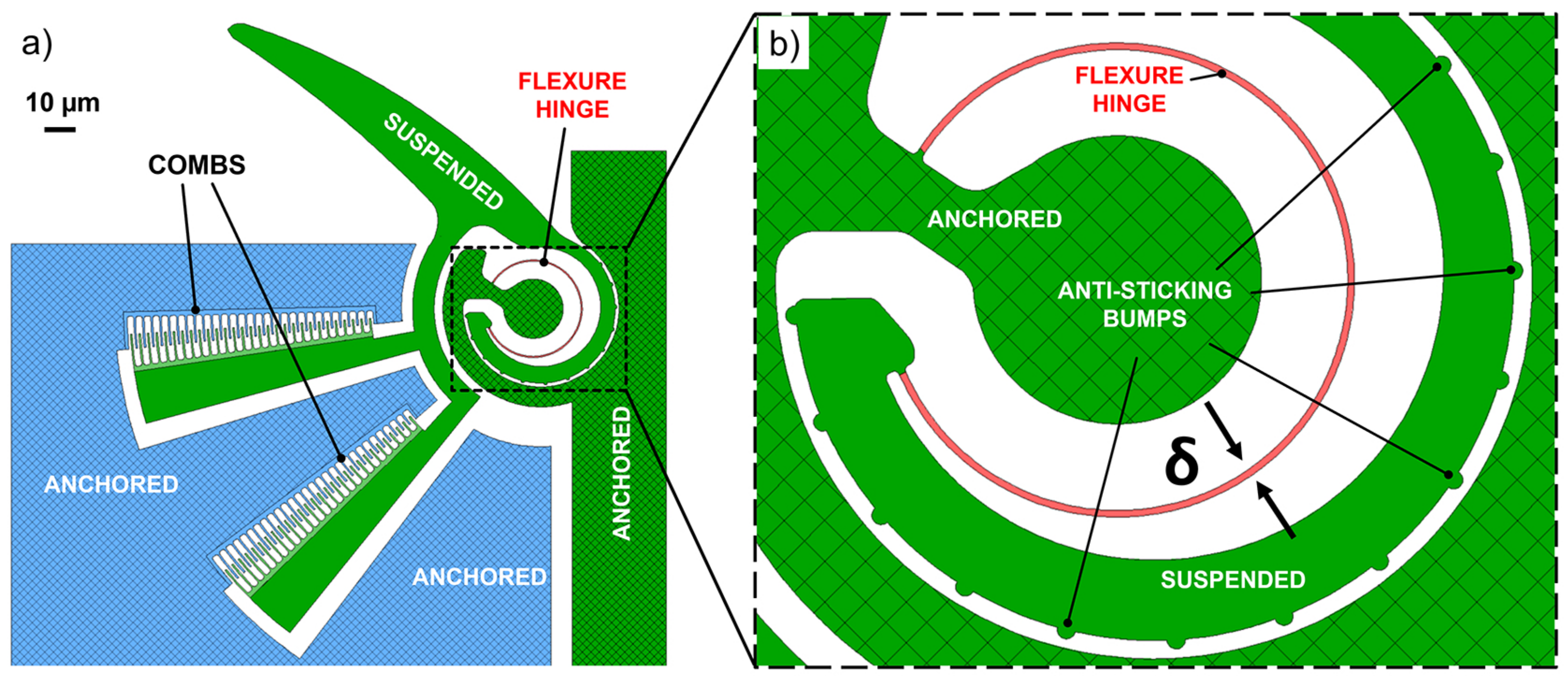
2. Design and Operating Principles

Complex compliant NEMS devices with electrostatic actuation [40] are the object of the present investigation. As a test case, the structure reported in Figure 1 has been adopted. This device covers a total area of (200 × 250) μ m 2 (excluding the pads). Figure 1a shows the top view, while an enlargement on the flexure hinge area is detailed in Figure 1b. The structure consists of a fixed part (that will be referred to as “anchored”) and a movable part (referred to as “suspended”). Two pairs of rotary combs [41] are able to exploit the capacitive effect between the two electrodes (green and blue in figure) and provide a torque with an applied voltage [42]. Each comb drive is composed of two curved arrays of interlocking fingers sectors, each finger being 0.8 μ m wide. Two adjacent fingers (from the two opposite sets) are separated by 1 μ m spacing. With no voltage applied, the fingers arrays have a 2° initial overlapping. The suspended component can move thanks to a lumped compliance flexure that, in the present case, consists of a simple 0.6 μ m-wide curved beam ( δ in Figure 1b), with a radius of 20 μ m. This shape determines a selective compliance because it induces mainly in-plane inflections around the preferred rotation axis. The Conjugate-Surfaces Flexure Hinge (CSFH) [43,44] has been provided with dimples consisting of anti-sticking bumps, in order to minimize sticking and friction phenomena between the surfaces of the conjugate surfaces [45,46]. The complete geometric features of the device are reported in Table 1.

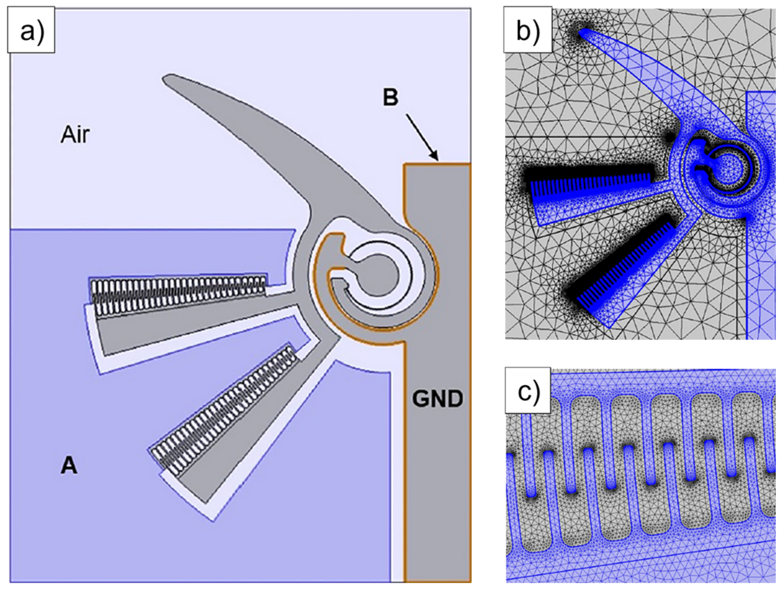
3. Numerical Approach

In the present investigation, the comb drive and the flexure hinge act as the two main components and, at the same time, as the two critical aspects of the device under study. The comb drive converts electrostatic energy into elastic potential energy, the latter one being stored by a progressive inflection of the curved beam. As a consequence, the flexure hinge enables the rotation of the device tip [47]. In this context, one of the most generally adopted geometrical parameters, critically important both for the comb drive and the flexure, is the well-known aspect ratio ρ , which is defined as u / δ , where u is the device layer thickness. The device’s characteristic width δ will be herein intended to be equal to the smallest geometric edge of the solid structure. Therefore, just for the sake of the present investigation, δ will be equal to the curved beam width (see Figure 1). Usually, ρ is regarded as one of the most relevant design parameters for MEMS technology based planar devices, and, in the examined case, it critically affects the in-planar flexures operational capabilities: the higher it is, the better [33].
The influence of the scaling effects on the device capabilities can be conveniently predicted theoretically before entering the prototyping stage [48]. However, if the geometry and the material configurations are complex, reliable predictions are very difficult to be carried out, risking partial or total failures. As a consequence, the need for iterating some fabrication steps gives rise to a great increase of the overall fabrication costs.
By introducing a down-scaling non–dimensional index β = δ ^ / δ as the ratio of an arbitrary width δ ^ = 0.6 μ m of the curved beam (at the initial scale), divided by the actual (variable) width δ , a numerical approach can be introduced to develop new design charts that could be used to reduce the number of attempts in prototyping.
This method can be summarized by the following phases:
  • preparation of the device model for the electromechanical simulations;
  • applications of the voltage between the electrodes for a variety of values;
  • determination of the voltage variability ranges due to the presence of critical voltage values; such ranges depend on the pull-in voltages [49] at which the fingers may induce short-circuits because of instability effects;
  • analysis of the device response in terms of motion, as well as of mechanical stress;
  • iteration of the procedure for different sets of β and ρ values;
  • mapping of the results with the limits due to the fabrication process;
  • arranging the design charts to offer a friendly display of the scaling effects on the device performances.
The electromechanical simulations have been carried out using COMSOL Multiphysics® 5.4. The electromechanics physics module models the electrostatic-mechanical coupling and solves the structural and electrostatic equations at once. A movable mesh node was also employed to account for the deformation of the air domain mesh, which allowed us to consider the electrostatic interaction between the comb-drive fingers in the air. The displacement of the mesh has been solved using the hyperelastic smoothing method. Several scaling factors within the range 0.2 ≤ β ≤ 15 were adopted assuming δ = 0.6 μ m as reference parameter for β = 1. Values of ρ equal to 1, 2 and 5 were chosen to examine the device response at different aspect ratios. Both the normal and the von Mises Stress equivalent criteria have been adopted to study the device mechanical strength. The von Mises yield criterion is used to predict yielding of materials that are subject to complex loading conditions, once the results of the uniaxial tensile tests are known, assuming that two stress states with equal distortion energy have an equal von Mises stress. The maximum normal stress criterion, chiefly used for brittle materials, is based on the assumption that failure occurs when the maximum principal stress reaches the ultimate strength of the material for simple tension.
Two performance indices were considered to assess the device electromechanical performances:
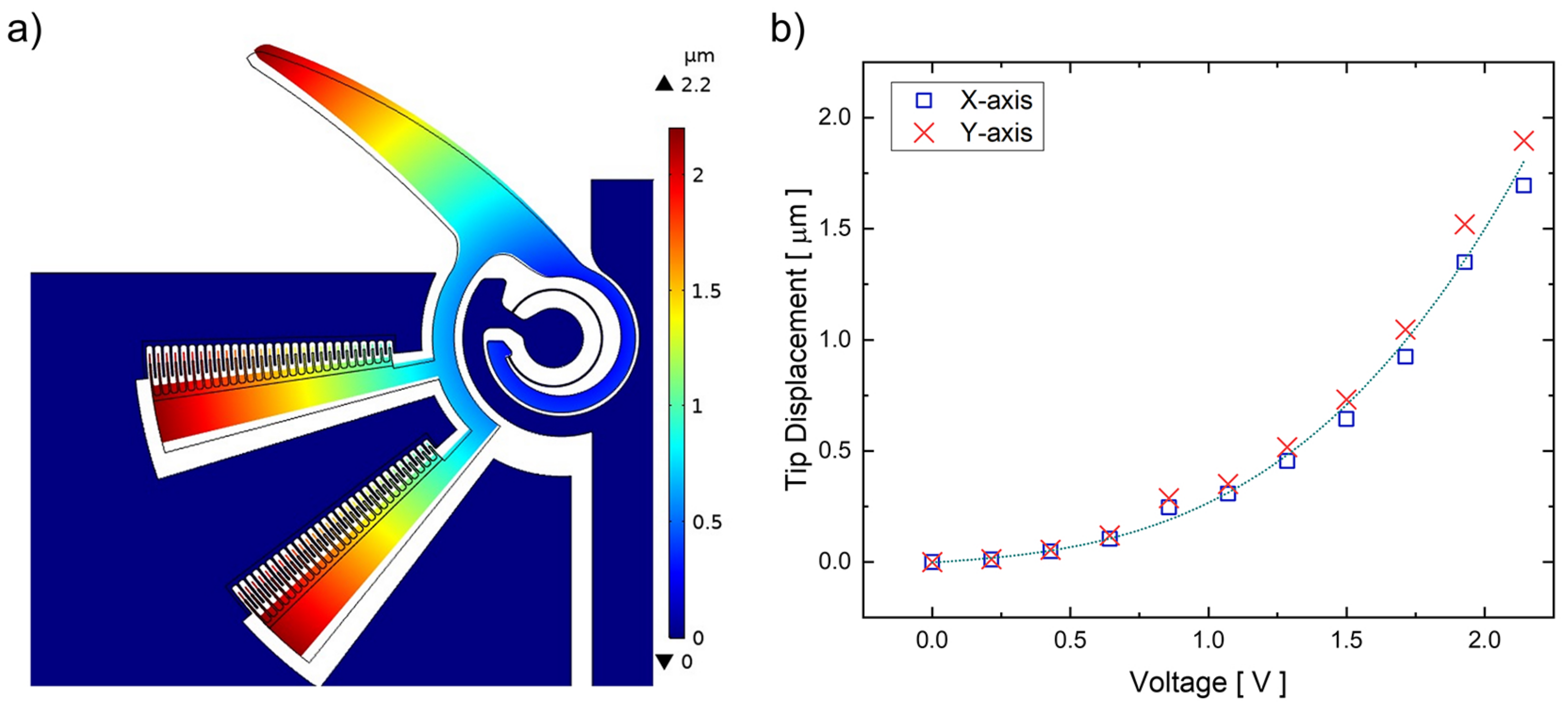
  • the maximum operating voltage that the comb configuration is able to sustain with no pull-in occurrence;
  • the device maximum sensitivity in terms of angular displacement per unit Volt (°/V).
The electric and mechanical boundary conditions are highlighted in Figure 2a. The pad with non-moving fingers (A) is supplied with voltage V and is mechanically fixed. The edges (B) are fixed and the whole moving part of the device is grounded (V = 0 V). The maximum and minimum mesh element sizes were set to secure the same number of elements for each analyzed scaling factor β .
The overall mesh consists of 89,100 triangular elements (Figure 2b,c), with quadratic serendipity geometry shape function. The direct solver MUMPS, configured in a segregated approach, has been used to solve the model. The relative tolerance for the error was set to 0.001. For each set of geometric parameter ( β , ρ ) and a single voltage value, the simulation time is variable (around 2 min on portable computers equipped with Intel® Core i7 8th generation CPU and 16 GB RAM).
The nanosystem is made of silicon and the anisotropic elasticity formulation was considered in the Finite Element simulations. The anisotropic stiffness coefficients of Si ⟨100⟩ was inferred from [50] and reported in Table 2 together with further specifications of the materials considered in the simulations. The nonlinearity due to large deflections was also taken into account.

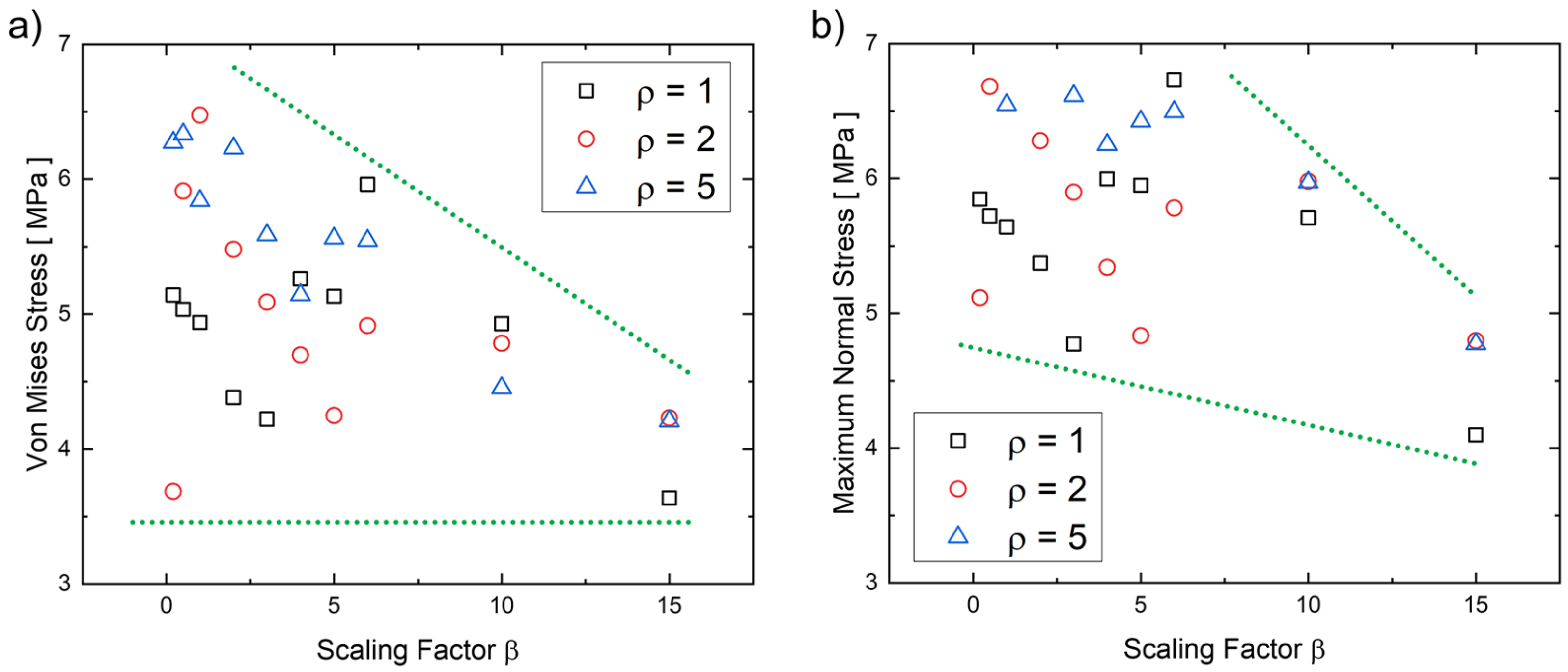
4. Results and Discussion

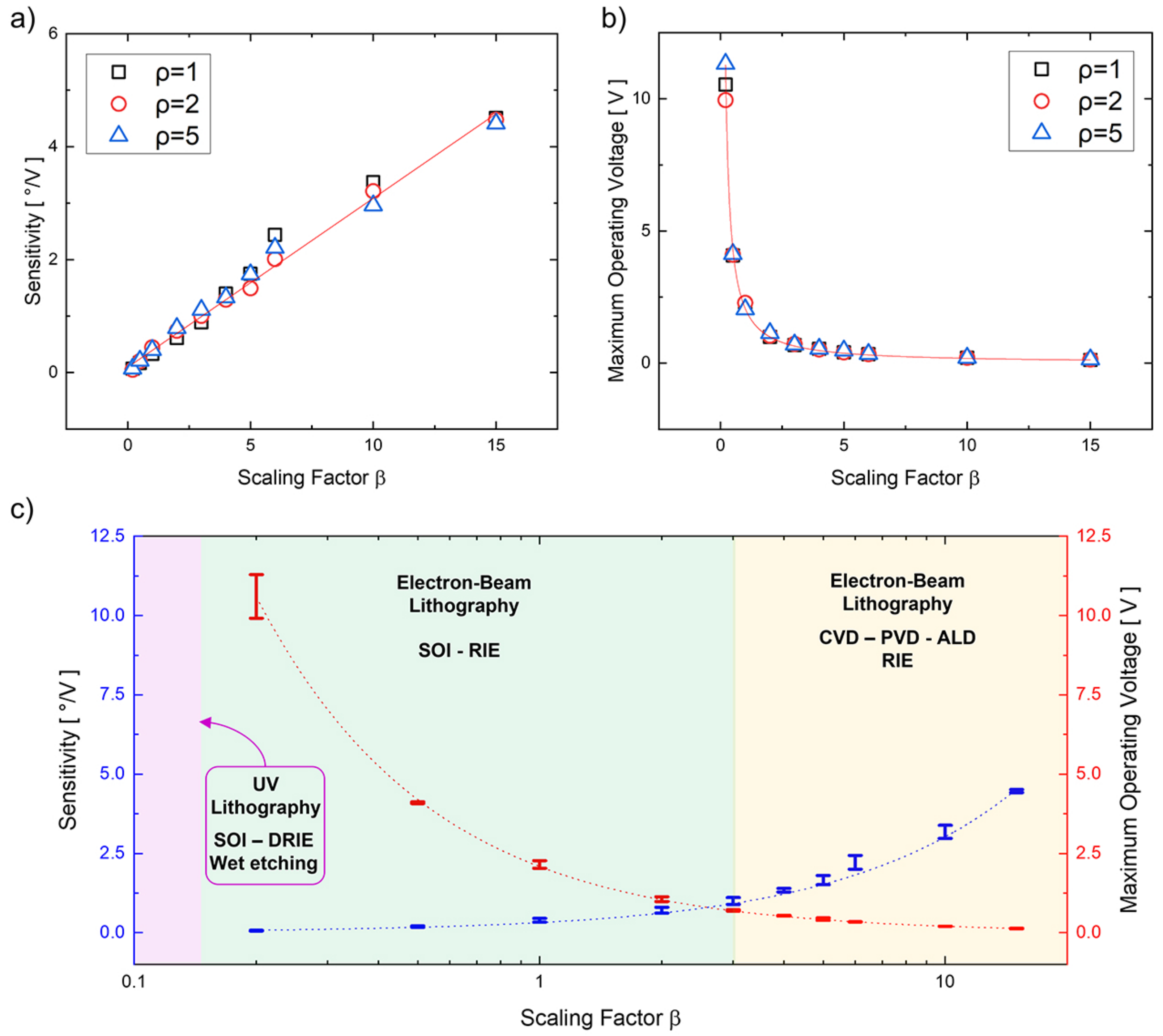
4.1. Numerical Results

Figure 3a shows the total displacement of the structure at its maximum bearable actuation voltage (in this case, equal to 2.14 V), considering a unitary aspect ratio ( ρ = 1) and β equal to 1. At the same ρ and β , Figure 3b reports the x and y components of the tip displacement (respectively acting along horizontal and vertical directions) at different actuation voltages.
Figure 3b shows that the device tip displacement grows quadratically with the supply voltage, as expected for electrostatically actuated comb-drives [51]. With the aim of studying the impact of β and ρ on the proposed device performance, a series of incremental numerical simulations have been planned and carried out. Firstly, the pull-in voltages were evaluated for each combination of scaling factor and aspect ratio. Table 3 has been built by calculating thirty values of the pull-in voltages for thirty combinations of ten scaling factors β by three values of the aspect ratio ρ . These data show that the pull-in voltage depends more on β than on ρ .
After assessing the pull-in phenomenon, the maximum operating voltage was then considered as 90% of the pull-in voltage, in order to study the stresses suffered by the structure. Figure 4a shows the maximum von Mises stress evaluated at the most critical part of the device, here correspondent to the curved flexure hinge, for several scaling factors β and aspect ratios ρ . The maximum normal stress is also considered and plotted in Figure 4b. According to the device material behaviour, ductile or brittle [52], the designer may conveniently refer to the von Mises stress or maximum normal stress data, respectively. However, it can be observed that, for the two criteria, a negative linear tendency appears weakly with a rather highly scattered pattern around an average value of 5 MPa which is way below the material tensile strength (i.e., 170 MPa). The lack of accuracy could be due to the fact that the stress evaluation is performed close to the pull-in voltage, a region where the MEMS behaviour is strongly nonlinear and unstable. It is worth noting that the von Mises and normal stress data scattering is not homogeneous for the considered cases. In fact, data present higher scattering for the cases ρ = 1 and ρ = 2 than for the case ρ = 5 . This phenomenon is probably due to the fact that, since the curved beam is a little more robust, the phenomena of numerical instability are less evident. To cope with the problem of data scattering, and considering that a slight convergent trend can be observed for increasing β values, a pair of green dotted lines has been added to both figures for a more immediate interpretation of the phenomena. From a stress point of view, these plots reveal how the designer can rely on a good materials and mechanics synthesis for a given scale, without potentially incurring in divergent behaviors or abrupt changes by orders of magnitude if any scale variation is needed.
Afterwards, the ways β and ρ affect the performances of the actuator were examined. For this purpose, the motion sensitivity to the actuation voltages, defined as the rotation (expressed in degrees) experienced by the comb-drives per unit of Volt supplied to the device, and the maximum operating voltage were evaluated for different β and ρ values. The outcomes are illustrated within the design chart reported in Figure 5. The plots display that the device sensitivity increases linearly with downsizing (Figure 5a). On the other hand, the maximum operating voltage hyperbolically decreases with β (Figure 5b). It is worth noting that the aspect ratio seems to have no significant impact on the device’s sensitivity, and only a limited impact (variation of about 6.8%) on the maximum operating voltages for relatively low β values (equal to 0.2), corresponding to relatively big geometries scale ( δ = 3 μ m).
From a technological standpoint, as reported in Figure 5c, if bigger scales are chosen ( β equal to 0.2 or 0.5), consolidated fabrication methods can be used to obtain a prototype: UV-lithography can be used to pattern the geometries on Silicon-on-Insulator (SOI) substrates [53]. If downscaling is needed, electron-beam lithography (EBL) must be used for accurate definition of sub-micrometre geometries [54]; moreover, since our results display no major changes when varying the aspect ratio, thinner structures can be considered for the same purpose. Therefore, Chemical Vapor Deposition (CVD), as well as Atomic Layer Deposition (ALD) or Epitaxial Growth, can be employed for its fabrication [55] (more details in the next section). Such results are believed to be useful to identify the optimal sizing of a MEMS/NEMS device for a given technology, based on the desired performances. In fact, within the scope of a given application, with prescribed maximum angular displacement, maximum operating voltage and allowable workspace, the designer is oriented toward the most appropriate fabrication process. For example, if the voltage amplitude and overall device size are not critical and large rotations (up to 2°) are involved, it is worthwhile to enlarge the device under examination and prefer consolidated fabrication methods in order to contain its corresponding costs. Conversely, if the overall device size is forced to be extremely scaled, higher device sensitivity and narrower voltage operating ranges should be expected. Such systems eventually require more demanding fabrication technologies, higher costs and, consequently, different applications’ spectra.

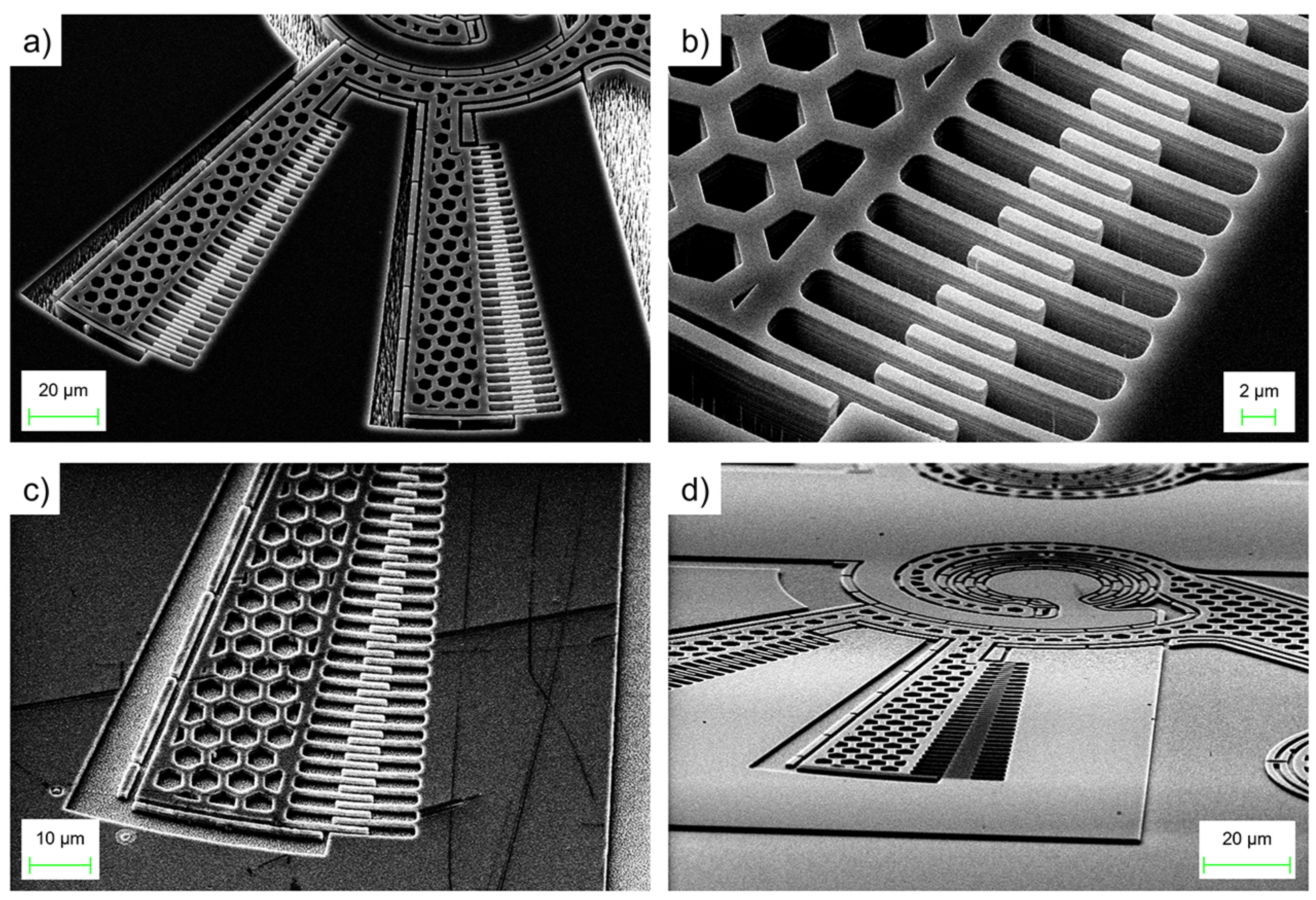
4.2. Technological Demonstration

Different fabrication procedures were employed to manufacture prototypes of the studied design. Figure 6 shows several Scanning Electron Microscope (SEM) pictures of the structure under analysis for β equal to 1. If a high aspect ratio is required for the proper functioning of the device, a Silicon-on-Insulator (SOI) substrate with a relatively thick device layer and Deep Reactive Ion Etching (DRIE) patterning are most likely to be adopted. SOI technology was originally conceived for integrated circuits [56] and then chosen for a wide range of applications, from MEMS sensors and actuators to integrated photonics [57,58]. Nowadays, SOI is a consolidated method and uses DRIE as a crucial patterning step, consisting of an anisotropic etch of silicon that can reach significantly high depths by exploiting the plasma phenomenon [59]. This is the case of Figure 6a,b, whose SEM pictures refer to a SOI substrate where a device depth of about 10 μ m was obtained by means of DRIE, achieving an aspect ratio of 16.6.
If lower aspect ratios can be tolerated, the deposition of a thinner film, using low-cost materials (such as amorphous silicon) and methods (such as Chemical Vapor Deposition, CVD) on low-cost substrates (such as glass) can be considered, and patterning by Reactive-Ion Etching (RIE) can be performed [32,60]. Amorphous silicon has been extensively studied and implemented in applications where low costs and technological versatility are crucial, such as solar cells or flexible electronics [61,62]. It is patterned using RIE, which adopts the same method but with less process steps, less expensive machinery, and simpler recipes [63]. This is the case for Figure 6c,d, whose SEM pictures refer to a glass substrate where a-Si has been deposited by CVD and a device depth of about 1.5 μ m was obtained by means of RIE, achieving an aspect ratio of 2.5.
All these concepts demonstrate that, depending on the desired performances, different strategies can be implemented for MEMS/NEMS prototyping. In the examined case, a more consolidated approach, such as SOI, can be seen as mandatory at first glance. However, a simple and fast numerical procedure shows how overall performance and functioning cannot be substantially hindered by lowering the device’s aspect ratio; this enables the usage of alternative methods to obtain thinner films and less complex patterning techniques, with the additional chance of widening its spectrum of applications.

5. Discussion

The structure maximum normal and von Mises stress has been defined in correspondence of the maximum bearable voltage in order not to incur into the pull-in state. This criterion is a rather arbitrary one, and therefore the reader must consider that different results could be obtained with a different definition. According to our choice, strength does not seem to be significantly dependent on downscaling. This suggests that a solid design which secures bearable stresses can be heavily downscaled without concern about major changes of responses to stress. In other words, the reported results, for the specific test case and the peculiar definition of the maximum bearable voltage, show how scaling does not significantly change the device’s response to mechanical stresses.
The device sensitivity, in terms of rotation degrees per unit volt applied, was observed to increase linearly with the downscaling. At the same time, the actuator’s maximum bearable voltage before pull-in was observed to decrease hyperbolically with downscaling.
In addition to this, the study has included analyses for different values of a structure’s aspect ratio, the latter being a crucial issue from both a technological (deep trenches fabrication) and functional (secure in-plane movement without out-of-plane inflections) standpoint: the evaluated performances in terms of sensitivity and maximum operating voltage display no significant changes when varying this parameter. In fact, significant improvements of the aspect ratio (2× and 5× the initial value) produce the same results having less than 5 % variation, with the sole exception of the maximum operating voltage at a scaling factor equal to 0.2 (6.8 % variation). This aspect invoked additional research on prototyping methods, and two technological strategies were examined: the first one, more consolidated and standard, is relying on relatively thicker crystalline silicon and SOI-DRIE; the second one, more unconventional and versatile, is relying on relatively thinner amorphous silicon and PECVD-RIE.

6. Conclusions

This work illustrated the impact of downscaling on the electromechanical functioning of a test case MEMS/NEMS Technology-based rotary comb drive actuator. An extensive numerical analysis, based on Finite Element Analysis, has been launched on the test device for different values of geometrical parameters. It was observed that the device sensitivity, in terms of rotation degrees per unit volt, increases linearly with downscaling. At the same time, the actuator maximum bearable voltage before pull-in was observed to be decreasing hyperbolically with downscaling. It was also found out that the device’s aspect ratio, which is a crucial parameter from the technological process standpoint, seems to yield negligible effects both on sensitivity and on the maximum operating voltage. In order to make these observations more clear, scaling-performance maps have been built, and herein presented, to be used as first aid design charts to reduce the prototyping time and costs. Finally, the structure stress analysis at the maximum operating voltage was performed for all the considered parameters combinations in order to verify the device structural integrity. It turned out that the maximum normal and von Mises stresses were not significantly affected by downsizing and their average values were around 5 MPa, which is far below the tensile strength of Silicon. In conclusion, the present study offered an example of development of a design chart that guides designers towards the choice of the most suitable technology, for the desired level of downscaling, and allows them to predict how the sensitivity and operating voltage would change with downsizing.

Author Contributions

Conceptualization and investigation, all authors; methodology, A.B., A.R. and N.P.B.; formal analysis, A.R. and N.P.B.; software and data curation, A.B., A.R. and E.G.; writing—original draft preparation, all authors; writing—review and editing, A.B., G.d.C. and N.P.B.; resources and supervision, E.G., G.d.C. and N.P.B. All authors have read and agreed to the published version of the manuscript.

Funding

This research received no external funding.

Institutional Review Board Statement

Not applicable.

Informed Consent Statement

Not applicable.

Data Availability Statement

No new data were created or analyzed in this study. Data sharing is not applicable to this article.

Conflicts of Interest

The authors declare no conflict of interest.

References

  1. Thompson, S.E.; Parthasarathy, S. Moore’s law: The future of Si microelectronics. Mater. Today 2006, 9, 20–25. [Google Scholar] [CrossRef]
  2. Thompson, S.E.; Chau, R.S.; Ghani, T.; Mistry, K.; Tyagi, S.; Bohr, M.T. In Search of “Forever,” Continued Transistor Scaling One New Material at a Time. IEEE Trans. Semicond. Manuf. 2005, 18, 26–36. [Google Scholar] [CrossRef]
  3. Frey, H. Handbook of Thin-Film Technology; Chapter Applications and Developments of Thin Film Technology; Springer: Berlin/Heidelberg, Germany, 2015; pp. 1–3. [Google Scholar] [CrossRef]
  4. Swain, N.; Venkatesh, V.; Kumar, P.; Srinivas, G.; Ravishankar, S.; Barshilia, H.C. Review on the machining characteristics and research prospects of conventional microscale machining operations. Mater. Manuf. Process. 2017, 32, 34–42. [Google Scholar] [CrossRef]
  5. Wise, K.D.; Najafi, K. Microfabrication Techniques for Integrated Sensors and Microsystems. Science 1991, 254, 1335–1342. [Google Scholar] [CrossRef] [PubMed] [Green Version]
  6. Judy, J.W. Microelectromechanical systems (MEMS): Fabrication, design and applications. Smart Mater. Struct. 2001, 10, 1115–1134. [Google Scholar] [CrossRef] [Green Version]
  7. Algamili, A.S.; Khir, M.H.M.; Dennis, J.O.; Ahmed, A.Y.; Alabsi, S.S.; Hashwan, S.S.B.; Junaid, M.M. A Review of Actuation and Sensing Mechanisms in MEMS-Based Sensor Devices. Nanoscale Res. Lett. 2021, 16, 16. [Google Scholar] [CrossRef]
  8. Poenar, D.P. Microfluidic and Micromachined/MEMS Devices for Separation, Discrimination and Detection of Airborne Particles for Pollution Monitoring. Micromachines 2019, 10, 483. [Google Scholar] [CrossRef] [Green Version]
  9. Verotti, M.; Dochshanov, A.; Belfiore, N.P. A Comprehensive Survey on Microgrippers Design: Mechanical Structure. J. Mech. Des. Trans. ASME 2017, 139, 060801. [Google Scholar] [CrossRef]
  10. Vargas-Chable, P.; Garcia, J.M., Jr.; Rodriguez-Fuentes, S.F.; Valle-Morales, S.I.; Tecpoyotl-Torres, M. Microgripper Based on Simple Compliance Configurations, Improved by Using Parameterization. Actuators 2020, 9, 140. [Google Scholar] [CrossRef]
  11. Vargas-Chable, P.; Tecpoyotl-Torres, M.; Cabello-Ruiz, R.; Rodriguez-Ramirez, J.; Vargas-Bernal, R. A Modified U-Shaped Micro-Actuator with a Compliant Mechanism Applied to a Microgripper. Actuators 2019, 8, 28. [Google Scholar] [CrossRef] [Green Version]
  12. Cauchi, M.; Grech, I.; Mallia, B.; Mollicone, P.; Sammut, N. The Effects of Structure Thickness, Air Gap Thickness and Silicon Type on the Performance of a Horizontal Electrothermal MEMS Microgripper. Actuators 2018, 7, 38. [Google Scholar] [CrossRef] [Green Version]
  13. Cauchi, M.; Grech, I.; Mallia, B.; Mollicone, P.; Portelli, B.; Sammut, N. Essential design and fabrication considerations for the reliable performance of an electrothermal MEMS microgripper. Microsyst. Technol. 2019, 1–16. [Google Scholar] [CrossRef]
  14. Cauchi, M.; Grech, I.; Mallia, B.; Mollicone, P.; Sammut, N. The effects of cold arm width and metal deposition on the performance of a U-beam electrothermal MEMS microgripper for biomedical applications. Micromachines 2019, 10, 167. [Google Scholar] [CrossRef] [PubMed] [Green Version]
  15. Pfusterschmied, G.; Kucera, M.; Wistrela, E.; Manzaneque, T.; Ruiz-Díez, V.; Sánchez-Rojas, J.; Bittner, A.; Schmid, U. Temperature dependent performance of piezoelectric MEMS resonators for viscosity and density determination of liquids. J. Micromech. Microeng. 2015, 25, 105014. [Google Scholar] [CrossRef]
  16. Ferrara-Bello, A.; Vargas-Chable, P.; Vera-Dimas, G.; Vargas-Bernal, R.; Tecpoyotl-Torres, M. XYZ Micropositioning System Based on Compliance Mechanisms Fabricated by Additive Manufacturing. Actuators 2021, 10, 68. [Google Scholar] [CrossRef]
  17. Qiao, Q.; Sun, H.; Liu, X.; Dong, B.; Xia, J.; Lee, C.; Zhou, G. Suspended silicon waveguide with sub-wavelength grating cladding for optical mems in mid-infrared. Micromachines 2021, 12, 1311. [Google Scholar] [CrossRef]
  18. Hahn, K.; Popp, J.; Wagener, A. Process management and design for MEMS and microelectronics technologies. In Microelectronics: Design, Technology, and Packaging; Abbott, D., Eshraghian, K., Musca, C.A., Pavlidis, D., Weste, N., Eds.; International Society for Optics and Photonics, SPIE: Perth, WA, Australia, 2004; Volume 5274, pp. 322–330. [Google Scholar] [CrossRef]
  19. Fedder, G.K.; Howe, R.T.; Liu, T.J.K.; Quevy, E.P. Technologies for Cofabricating MEMS and Electronics. Proc. IEEE 2008, 96, 306–322. [Google Scholar] [CrossRef]
  20. Ozaydin-Ince, G.; Coclite, A.M.; Gleason, K.K. CVD of polymeric thin films: Applications in sensors, biotechnology, microelectronics/organic electronics, microfluidics, MEMS, composites and membranes. Rep. Prog. Phys. 2011, 75, 016501. [Google Scholar] [CrossRef]
  21. Brand, O. Microsensor Integration Into Systems-on-Chip. Proc. IEEE 2006, 94, 1160–1176. [Google Scholar] [CrossRef]
  22. Varadan, V.; Varadan, V. Microsensors, microelectromechanical systems (MEMS), and electronics for smart structures and systems. Smart Mater. Struct. 2000, 9, 953–972. [Google Scholar] [CrossRef]
  23. Spearing, S. Materials issues in microelectromechanical systems (MEMS). Acta Mater. 2000, 48, 179–196. [Google Scholar] [CrossRef]
  24. Feynman, R.P. There’s plenty of room at the bottom. J. Microelectromech. Syst. 1992, 1, 60–66. [Google Scholar] [CrossRef]
  25. Roukes, M. Plenty of Room, Indeed. Sci. Am. 2001, 285, 48–57. [Google Scholar] [CrossRef] [PubMed]
  26. Zhu, J.; Liu, X.; Shi, Q.; He, T.; Sun, Z.; Guo, X.; Liu, W.; Sulaiman, O.B.; Dong, B.; Lee, C. Development trends and perspectives of future sensors and MEMS/NEMS. Micromachines 2020, 11, 7. [Google Scholar] [CrossRef] [PubMed] [Green Version]
  27. Roukes, M.L. Nanoelectromechanical systems face the future. Phys. World 2001, 14, 25–32. [Google Scholar] [CrossRef] [Green Version]
  28. Jianrong, C.; Yuqing, M.; Nongyue, H.; Xiaohua, W.; Sijiao, L. Nanotechnology and biosensors. Biotechnol. Adv. 2004, 22, 505–518. [Google Scholar] [CrossRef] [PubMed]
  29. Bhushan, B. Nanotribology and nanomechanics of MEMS/NEMS and BioMEMS/BioNEMS materials and devices. Microelectron. Eng. 2007, 84, 387–412. [Google Scholar] [CrossRef]
  30. Fraga, M.; Pessoa, R. Progresses in Synthesis and Application of SiC Films: From CVD to ALD and from MEMS to NEMS. Micromachines 2020, 11, 799. [Google Scholar] [CrossRef]
  31. Neuville, S. Selective Carbon Material Engineering for Improved MEMS and NEMS. Micromachines 2019, 10, 539. [Google Scholar] [CrossRef] [Green Version]
  32. Veroli, A.; Buzzin, A.; Crescenzi, R.; Frezza, F.; de Cesare, G.; D’Andrea, V.; Mura, F.; Verotti, M.; Dochshanov, A.; Belfiore, N.P. Development of a NEMS-technology based nano gripper. In Advances in Service and Industrial Robotics, Proceedings of the International Conference on Robotics in Alpe-Adria Danube Region, Torino, Italy, 21–23 June 2017; Springer: Cham, Switzerland, 2017; pp. 601–611. [Google Scholar] [CrossRef]
  33. Vurchio, F.; Ursi, P.; Buzzin, A.; Veroli, A.; Scorza, A.; Verotti, M.; Sciuto, S.A.; Belfiore, N.P. Grasping and releasing agarose micro beads in water drops. Micromachines 2019, 10, 436. [Google Scholar] [CrossRef] [Green Version]
  34. Luisetto, I.; Tuti, S.; Marconi, E.; Veroli, A.; Buzzin, A.; De Cesare, G.; Natali, S.; Verotti, M.; Giovine, E.; Belfiore, N.P. An Interdisciplinary Approach to the Nanomanipulation of SiO2 Nanoparticles: Design, Fabrication and Feasibility. Appl. Sci. 2018, 8, 2645. [Google Scholar] [CrossRef] [Green Version]
  35. Belfiore, N.P. Micromanipulation: A challenge for actuation. Actuators 2018, 7, 85. [Google Scholar] [CrossRef] [Green Version]
  36. Belfiore, N.P.; Bagolini, A.; Rossi, A.; Bocchetta, G.; Vurchio, F.; Crescenzi, R.; Scorza, A.; Bellutti, P.; Sciuto, S.A. Design, fabrication, testing and simulation of a rotary double comb drives actuated microgripper. Micromachines 2021, 12, 1263. [Google Scholar] [CrossRef] [PubMed]
  37. Hou, M.T.K.; Huang, J.Y.; Jiang, S.S.; Yeh, J.L.A. In-plane rotary comb-drive actuator for a variable optical attenuator. J. Micro/Nanolithogr. MEMS MOEMS 2008, 7, 043015. [Google Scholar] [CrossRef]
  38. Verotti, M.; Crescenzi, R.; Balucani, M.; Belfiore, N.P. MEMS-based conjugate surfaces flexure hinge. J. Mech. Des. 2015, 137, 012301. [Google Scholar] [CrossRef]
  39. Veroli, A.; Buzzin, A.; Frezza, F.; De Cesare, G.; Hamidullah, M.; Giovine, E.; Verotti, M.; Belfiore, N.P. An approach to the extreme miniaturization of rotary comb drives. Actuators 2018, 7, 70. [Google Scholar] [CrossRef] [Green Version]
  40. Buzzin, A.; Cupo, S.; Giovine, E.; de Cesare, G.; Belfiore, N.P. Compliant Nano-Pliers as a Biomedical Tool at the Nanoscale: Design, Simulation and Fabrication. Micromachines 2020, 11, 1087. [Google Scholar] [CrossRef] [PubMed]
  41. Xie, H.; Pan, Y.; Fedder, G.K. A CMOS-MEMS mirror with curled-hinge comb drives. J. Microelectromech. Syst. 2003, 12, 450–457. [Google Scholar] [CrossRef]
  42. Chang, C.M.; Wang, S.Y.; Chen, R.; Yeh, J.A.; Hou, M.T. A comb-drive actuator driven by capacitively-coupled-power. Sensors 2012, 12, 10881–10889. [Google Scholar] [CrossRef]
  43. Verotti, M.; Dochshanov, A.; Belfiore, N.P. Compliance synthesis of CSFH MEMS-based microgrippers. J. Mech. Des. 2017, 139, 022301. [Google Scholar] [CrossRef]
  44. Crescenzi, R.; Balucani, M.; Belfiore, N.P. Operational characterization of CSFH MEMS technology based hinges. J. Micromech. Microeng. 2018, 28, 055012. [Google Scholar] [CrossRef]
  45. Zhuang, Y.; Menon, A. On the stiction of MEMS materials. Tribol. Lett. 2005, 19, 111–117. [Google Scholar] [CrossRef]
  46. Van Spengen, W.M. MEMS reliability from a failure mechanisms perspective. Microelectron. Reliab. 2003, 43, 1049–1060. [Google Scholar] [CrossRef]
  47. Buzzin, A.; Veroli, A.; de Cesare, G.; Giovine, E.; Verotti, M.; Belfiore, N.P. A new NEMS based linear-to-rotary displacement-capacity transducer. In Proceedings of the 2019 IEEE 8th International Workshop on Advances in Sensors and Interfaces (IWASI), Otranto, Italy, 13–14 June 2019; pp. 201–204. [Google Scholar] [CrossRef]
  48. Dochshanov, A.; Verotti, M.; Belfiore, N.P. A comprehensive survey on microgrippers design: Operational strategy. J. Mech. Des. 2017, 139, 070801. [Google Scholar] [CrossRef]
  49. Zhang, W.M.; Yan, H.; Peng, Z.K.; Meng, G. Electrostatic pull-in instability in MEMS/NEMS: A review. Sens. Actuators A Phys. 2014, 214, 187–218. [Google Scholar] [CrossRef]
  50. Hopcroft, M.A.; Nix, W.D.; Kenny, T.W. What is the Young’s Modulus of Silicon? J. Microelectromech. Syst. 2010, 19, 229–238. [Google Scholar] [CrossRef] [Green Version]
  51. Sardan, O.; Alaca, B.E.; Yalcinkaya, A.D.; Bøggild, P.; Tang, P.T.; Hansen, O. Microgrippers: A case study for batch-compatible integration of MEMS with nanostructures. Nanotechnology 2007, 18, 375501. [Google Scholar] [CrossRef] [Green Version]
  52. Brede, M. The brittle-to-ductile transition in silicon. Acta Metall. Et Mater. 1993, 41, 211–228. [Google Scholar] [CrossRef]
  53. Dumon, P.; Bogaerts, W.; Wiaux, V.; Wouters, J.; Beckx, S.; Van Campenhout, J.; Taillaert, D.; Luyssaert, B.; Bienstman, P.; Van Thourhout, D.; et al. Low-loss SOI photonic wires and ring resonators fabricated with deep UV lithography. IEEE Photonics Technol. Lett. 2004, 16, 1328–1330. [Google Scholar] [CrossRef] [Green Version]
  54. Manfrinato, V.R.; Zhang, L.; Su, D.; Duan, H.; Hobbs, R.G.; Stach, E.A.; Berggren, K.K. Resolution limits of electron-beam lithography toward the atomic scale. Nano Lett. 2013, 13, 1555–1558. [Google Scholar] [CrossRef]
  55. Biswas, A.; Bayer, I.S.; Biris, A.S.; Wang, T.; Dervishi, E.; Faupel, F. Advances in top–down and bottom–up surface nanofabrication: Techniques, applications & future prospects. Adv. Colloid Interface Sci. 2012, 170, 2–27. [Google Scholar] [CrossRef]
  56. Rudenko, T.; Nazarov, A.; Lysenko, V. The advancement of silicon-on-insulator (SOI) devices and their basic properties. Semicond. Phys. Quantum Electron. Optoelectron. 2020, 23, 227–252. [Google Scholar] [CrossRef]
  57. Dao, D.V.; Nakamura, K.; Bui, T.T.; Sugiyama, S. Micro/nano-mechanical sensors and actuators based on SOI-MEMS technology. Adv. Nat. Sci. Nanosci. Nanotechnol. 2010, 1, 013001. [Google Scholar] [CrossRef]
  58. Zortman, W.A.; Trotter, D.C.; Watts, M.R. Silicon photonics manufacturing. Opt. Express 2010, 18, 23598–23607. [Google Scholar] [CrossRef] [Green Version]
  59. Wu, B.; Kumar, A.; Pamarthy, S. High aspect ratio silicon etch: A review. J. Appl. Phys. 2010, 108, 9. [Google Scholar] [CrossRef]
  60. Buzzin, A.; Veroli, A.; De Cesare, G.; Belfiore, N. NEMS-technology based nano gripper for mechanic manipulation in space exploration mission. Adv. Astro. Sci. 2018, 163, 61–67. [Google Scholar]
  61. Yoshikawa, K.; Kawasaki, H.; Yoshida, W.; Irie, T.; Konishi, K.; Nakano, K.; Uto, T.; Adachi, D.; Kanematsu, M.; Uzu, H.; et al. Silicon heterojunction solar cell with interdigitated back contacts for a photoconversion efficiency over 26%. Nat. Energy 2017, 2, 1–8. [Google Scholar] [CrossRef]
  62. Nomura, K.; Ohta, H.; Takagi, A.; Kamiya, T.; Hirano, M.; Hosono, H. Room-temperature fabrication of transparent flexible thin-film transistors using amorphous oxide semiconductors. Nature 2004, 432, 488–492. [Google Scholar] [CrossRef] [PubMed]
  63. Winderbaum, S.; Reinhold, O.; Yun, F. Reactive ion etching (RIE) as a method for texturing polycrystalline silicon solar cells. Sol. Energy Mater. Sol. Cells 1997, 46, 239–248. [Google Scholar] [CrossRef]
Figure 1. (a) Top view of the studied system: voltage is applied between the anchored blue and green pads to provide motion through the comb drives and the flexure hinge; (b) enlargement on the CSFH site.
Actuators 11 00071 g001
Figure 2. (a) 2D model mechanical and electrical boundary conditions of the device under examination: the pad (A) is anchored and supplied with a potential V, the edges (B) (highlighted in yellow color) are fixed and the entire device is electrically grounded (GND). (b) generated mesh; (c) mesh details of the interdigitated fingers.
Actuators 11 00071 g002
Figure 3. (a) Device total displacement distribution for V = 2.14 V and ρ = 1, β = 1; (b) device tip x and y displacement vs. voltage supply ( ρ = 1, β = 1).
Actuators 11 00071 g003
Figure 4. (a) Maximum von Mises stress reached at the most critical section for several scaling factors β and aspect ratios ρ ; (b) maximum normal stress reached at the most critical section for several scaling factors β and aspect ratios ρ .
Actuators 11 00071 g004
Figure 5. (a) Device sensitivity vs. scaling factor β evaluated for different aspect ratios ρ ; (b) maximum operating voltage vs. scaling factor β evaluated for different aspect ratios ρ ; (c) design chart with the two behaviors plotted in the form of mean and standard error and including technological solutions for three different scaling macroareas.
Actuators 11 00071 g005
Figure 6. (a) SEM picture the structure under analysis, obtained with SOI technology after the DRIE patterning process, 45° tilted view; (b) 45° tilted enlargement on the comb fingers; (c) SEM picture of the structure under analysis obtained with a-Si after the RIE patterning process, 45° tilted view; (d) 70° tilted view of the device.
Actuators 11 00071 g006
Table 1. Comb-drive and CSFH design specifications.
ComponentFeatureValue
Comb-driveNumber of fingers29
Fingers width0.8 μ m
Fingers minimum length5.5 μ m
Fingers maximum length12.5 μ m
Fingers radial spacing2.8 μ m
Rotor-Stator fingers distance1 μ m
Initial overlapping angle2
Maximum comb-drive angular displacement2.5
CSFHCurved beam length106 μ m
Curved beam width0.6 μ m
Curvature radius20 μ m
Table 2. Materials’ specifications.
Si ⟨100⟩
PropertyValueUnit
c 11 165.6GPa
Stiffness coefficients c 12 63.9GPa
c 44 79.5GPa
Tensile strength σ s 170MPa
Relative permittivity ϵ r 11.9
Density ρ 2320 kg m 3
Poisson’s ratio ν 0.22
Specific heat c p 680 J kgK
Operative temperature T r 298.15K
Air
Density ρ 1.225 kg m 3
Specific heat c p 1005 J kgK
Relative permittivity ϵ r 1
Table 3. Pull-in voltages for different combinations of scaling factor β and aspect ratio ρ .
Scaling Factor (β)Pull-in Voltage (V)
ρ = 1 ρ = 2 ρ = 5
0.211.7111.0612.58
0.54.534.564.59
12.382.532.27
21.111.151.27
30.760.810.78
40.600.580.61
50.450.450.53
60.380.380.39
100.230.230.23
150.130.150.15
Publisher’s Note: MDPI stays neutral with regard to jurisdictional claims in published maps and institutional affiliations.

