Abstract
Existing piezoelectric vibration energy harvesting circuits require auxiliary power for the switch control module and are difficult to adapt to broadband piezoelectric vibration energy harvesters. This paper proposes a self-powered and low-power enhanced double synchronized switch harvesting (EDSSH) circuit. The proposed circuit consists of a low-power follow-up switch control circuit, reverse feedback blocking-up circuit, synchronous electric charge extraction circuit and buck-boost circuit. The EDSSH circuit can automatically adapt to the sinusoidal voltage signal with the frequency of 1 to 312.5 Hz that is output by the piezoelectric vibration energy harvester. The switch control circuit of the EDSSH circuit works intermittently for a very short time near the power extreme point and consumes a low amount of electric energy. The reverse feedback blocking-up circuit of the EDSSH circuit can keep the transmission efficiency at the optimal value. By using a charging capacitor of 1 mF, the charging efficiency of the proposed EDSSH circuit is 1.51 times that of the DSSH circuit.
1. Introduction
The self-powered wireless sensor which can automatically obtain electric energy from ambient vibration has great application prospects in the field of structural health detection [,,]. It is important to develop an efficient self-powered system which can automatically convert environmental vibration energy into electric energy for the application of wireless sensors. Piezoelectric smart structures have been widely studied in the field of ambient vibration energy harvesting because of their sensitivity to vibration, high energy density [,] and high output voltage [,]. The research on piezoelectric vibration energy harvesting systems mainly includes three aspects: the modeling theory and method, the mechanical structure optimization design and the energy harvesting interface circuit.
Researchers have deeply investigated the modeling theory and methods of piezoelectric vibrators. Some analytical models are already available in the literature. Erturk and Inman [,] established an analytical distributed parameter model for cantilevered piezoelectric energy harvesters. Liao and Sodano [,] developed a theoretical model of a piezoelectric energy harvesting system to predict the power around a single vibration mode based on the Rayleigh–Ritz approach. Fakharian and Salmani [] researched a lumped parameter model for an exponentially tapered piezoelectric beam in transverse vibration. Kärki [], Baishya [], Wang [], Sriramdas [] and Rammohan [] studied a lumped-parameter transducer model for piezoelectric and ferroelectric polymers. Elvin [,] proposed a general equivalent circuit model for piezoelectric generators and a coupled finite element-circuit simulation model for analyzing a piezoelectric energy generator. Roundy [] established a distributed parameter model for improving power output for vibration-based energy scavengers. Yang and Tang [] established an equivalent circuit modeling of piezoelectric energy harvesters. Wang [], Zhang [], Ko [] and Saleem [] investigated modeling and parameter identification for equivalent circuit modeling of piezoelectric energy harvesters with theoretical analysis. Noël [], He [], Wang [], Xie [] and Billings [] put forward a method of modeling and parameter identification for the circuit model of a nonlinear piezoelectric vibrator.
Several methods have been proposed by researchers to improve the energy conversion efficiency and expand the band of the operation frequency of VEHs. One of the approaches is frequency tuning, such as mechanical tuning [,,,,], circuit tuning and magnetic tuning [,,,]. This strategy allows VEHs to adjust their resonant frequency according to the environmental vibration frequency. However, this increases the complexity or consume extra energy of the VEHs. For instance, Eichhorn [] proposed a piezoelectric energy harvesting structure of a cantilever beam with additional mechanical mass, which changes the resonant frequency of the structure by applying pressure or tensile force to the cantilever beam. Fan [] designed a vibration energy harvester that composed of a piezoelectric harvester, stopper and magnet. The system can tune the vibration energy harvester to a lower working frequency range by changing the gap between mass and magnets, so as to improve the efficiency of energy collection. Another approach is to use multi-modal energy capture technology with different resonant frequencies, including generator arrays [,,,] and coupled vibration [,,,,,]. Although coupled vibration is easy to achieve, the maximum output power of the VEH is consequently reduced. Nabavi [] proposed a piezoelectric MEMS harvester with symmetrical and double clamping structure, which has multi-mode and nonlinear characteristics and effectively broadens the working bandwidth. Hu [] proposed a broadband multi mass and multi spring piezoelectric vibration energy harvester based on a folded asymmetric gap cantilever beam, which can make each stage of pure bending form multiple resonance modes. The working frequency band of the structure is widened effectively. Recently, nonlinear vibration energy harvesting approaches, for instance, nonlinear magnetic coupling [,,,,,,] and piecewise-linear structure [,,,], have attracted the interest of researchers. Although energy conversion efficiency of the unit volume material is decreased, the operation frequency band of the VEH could be widened.
There are special requirements for piezoelectric energy harvesters (PEHs) and their electric energy harvesting circuits due to the wide range of vibration frequency and large load range of actual working environment. Therefore, a low-power high-efficiency adaptive energy harvesting circuit which can match the PEH with wide operation frequency band and load range is the key to the practical application of the piezoelectric system.
The standard energy harvesting (SEH) [,] interface circuit was first reported as a power harvesting circuit of PEHs for its simple structures and needless of external control module, but the energy harvesting efficiency is low and obviously affected by load. Lefeuvre [] proposed a two-stage interface circuit of the down-to-step voltage converter, which has low power and can charge a 4.8 V rechargeable battery efficiently. Garbuio and Guyomar [,,] investigated the synchronized switch harvesting on inductor (SSHI) technique for vibration control of piezoelectric structures, which adds synchronous switching damping at both ends of piezoelectric elements to improve the efficiency of energy harvesting. The SSHI scheme uses an LC resonant circuit for capacitor charging to reduce energy loss. Liang and Badel [,] proposed a synchronous switch damping technology by adding series inductors in the circuit, in which the synchronous switch is used to quickly flip the piezoelectric voltage and improve the energy conversion efficiency. Shu, Ramadass, Lefeurve and Lallart [,,,] developed the Seris-SSHI (S-SSHI) and the parallel-SSHI (P-SSHI) technologies further, but the circuit scheme requires impedance matching to achieve maximum power transmission and can only match the load in a narrow range. Lefeuvre [], Gasnier [] and Dini [] studied the SSHI technology and proposed synchronous electric charge extraction (SECE) technology. The energy harvesting efficiency of the SECE scheme is independent of the load, and the range of matching loads is wide for the use of the LC resonant circuit to transfer the power of the PEH to the inductor and then to the load through the DC-DC converter in the SECE scheme.
Recently, researchers proposed a class of double synchronized switch harvesting (DSSH) [,,] circuits as shown in Figure 1 by optimizing the control of switches of SECE to make the circuit more efficient. Wang [] analyzed a self-powered, ultra-low-power control circuit for weak coupling and heavy load. Wu [] used two resonant rings to flip the capacitor voltage in each half cycle to improve the power harvesting efficiency of an SSHI circuit. Din [] designed an energy harvesting circuit based on MOS devices to reduce power consumption. Chen [] reported a fast self-starting and low-power management circuit for a micro piezoelectric energy harvester. Lallart [] studied a nonlinear technology and self-powered circuit to harvest energy from PEHs under no-load conditions efficiently. The main shortcomings of the DSSH circuit are the complexity of the switch control, the need for an additional switch control circuit and auxiliary power supply, and the low conversion efficiency due to the inaccurate switch time control. To the best of our knowledge, existing solutions have either low energy harvesting efficiency such as the SEH circuit [,], are unable to sufficiently match loads such as P-SSHI and S-SSHI circuits [,,,,,] or are excessively complicated and require auxiliary power for the switch control circuit [,,].

Figure 1.
Schematic diagram of the DSSH circuit.
This paper proposes a low-power high-efficiency adaptive double synchronized switch harvesting circuit for broadband PEHs based on DSSH called an enhanced double synchronized switch harvesting (EDSSH) circuit. The schematic diagram is shown in Figure 2. The EDSSH circuit has four advantages. First, compared with DSSH, the EDSSH circuit simplifies the switching control circuit, reduces the power consumption of the switching control circuit and does not need a special auxiliary power supply. Moreover, in order to reduce the power consumption, the switch control circuit is in the sleep state most of the time and starts automatically only for a short time near the power extreme point. Secondly, the EDSSH circuit adds a power reverse feedback blocking-up circuit (RFBC) into DSSH to keep the energy harvesting efficiency optimal and avoid the problem of unstable energy harvesting efficiency of the DSSH circuit. Thirdly, the EDSSH circuit inherits the power extreme value tracking point technology of DSSH, which has stronger energy harvesting efficiency than SEH and SSHI circuits. Lastly, it can automatically adapt to input voltage signals with a wide frequency range.

Figure 2.
Schematic diagram of EDSSH circuit.
2. The Proposed EDSSH Circuit
2.1. Structure of EDSSH Circuit
The proposed EDSSH circuit is shown in Figure 2. The simulation circuit according to the schematic diagram of the EDSSH circuit is shown in Figure 3. The circuit includes a PEH, a rectifier bridge, an energy transfer circuit composed of S1-L1-D5-Ci-S2-D6, a buck-boost circuit, the control circuit of switch S1 and the control circuit of switch S2. The PEH part is represented by an AC voltage source VP (12.26 V, 50 Hz) and a capacitance CP (62.36 nF).
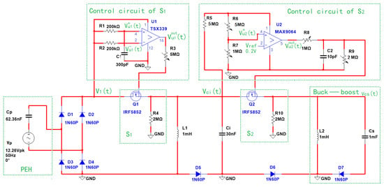
Figure 3.
Simulation circuit of the EDSSH circuit.
The EDSSH circuit consists of four working circuits:
- (1)
- The first circuit loop is composed of the capacitor CP, rectifier bridge D1-D4, inductor L1, ultra-low on-resistance MOSFET Q1 (representative switch S1) and control circuit of S1. This circuit is used to harvest the electric energy generated by the PEH. Compared with DSSH, the EDSSH circuit has three improvements. First, the EDSSH circuit simplifies the switching control circuit and uses a simple structure and low-power IC, a comparator TSX339, three resistors and one capacitor. The control circuit of S1 is composed of the micro-power quad CMOS voltage comparator TSX339 and its peripheral circuit. The no-inverting input terminal of TSX339 is connected to through the RC signal delay circuit (delay time TC = R1∗C1). The inverting input terminal of TSX339 is connected to through the current limiting resistor R2. The terminal Vcc is connected to directly. The ground terminal of TSX339 is grounded. The output terminal of TSX339 is connected to the gate terminal of Q1 through an adjustable resistor R3. Secondly, other passive components are also low power consumption. The rectifier bridge D1-D4 is composed of four ultra-low-power IN60P diodes with forward voltage of 0.24 V, reverse voltage of 40 V and maximum forward current of 50 mA. The controlled switch S1 is represented by N-channel MOSFET IRF5852 with ultra-low static drain-to-source on-resistance of , switch frequency exceeding 108/s and minimum drain-to-source breakdown voltage () of 20 V. Thirdly, the control circuit of S1 with low power and low-cold-start threshold does not need additional power supply but is supplied by the output voltage of the rectifier bridge. The control circuit of S1 can automatically control S1 turn on for a brief time when the voltage of reaches the extreme value and consumes very little power. That is, TSX339 compares the voltage of the no-inverting input terminal and inverting input terminal in real time. When the voltage of the no-inverting input terminal is higher than that of the inverting input terminal at the peak value of , is output directly through the output terminal of TSX339 to control Q1 turn on for a short time. When the output voltage () drops from a high value to the drain-source on-voltage of IRF5852, Q1 turns off automatically. During this short time, electric energy is transferred from Cp to L1.
- (2)
- The second circuit loop is composed of inductor L1, capacitor Ci and diode D5. Compared with DSSH, the EDSSH circuit sets a low-power diode D5 in this circuit loop, which together with Ci and L1 forms the reverse feedback blocking-up circuit (RFBC). It avoids the unstable power transfer efficiency of DSSH caused by L1-Ci oscillation and ensures that power is only transferred from inductor L1 to the capacitor Ci in one way.
- (3)
- The capacitor Ci, inductor L2, diode D6, ultra-low on-resistance MOSFET Q2 (representative switch S2) and the control circuit of S2 constitute the third circuit loop. Compared with DSSH, the EDSSH circuit has three improvements. First, the EDSSH circuit simplifies the switching control circuit and uses a simple structure and low-power IC, a comparator MAX9064, five resistors and one capacitor. The control circuit of S2 is composed of the low-power comparator MAX9064 and its peripheral circuit. The inverting input terminal does not need a reference voltage source due to its internal Vref (0.2 V). Because the range of VCC of MAX9064 is 0.9 to 5.5 V, but reaches 14 V, is connected to the no-inverting input of MAX9064 after depressurization through series resistance R5, R6 and R7. Secondly, other passive components also have low power consumption, such as ultra-low on-resistance MOSFET Q2 and diode D6 (IN60P). Thirdly, the control circuit of switch S2 with low power and does not need an additional power supply but is supplied by the output voltage , and it can control S2 turn on when the voltage of reaches the maximum after a brief time, and S2 turns off when the current in the inductor L2 reaches the maximum. That is, when the reaches the maximum (at this time, the no-inverting input voltage of MAX9064 just exceeds its Vref (0.2 V)), MAX9064 outputs high voltage for a short time () and controls S2 turn on. The is determined by the discharge time of the RC discharge circuit composed of R9 and C2, and it must be equal to one fourth of the oscillation period of the LC oscillation circuit composed of L2 and Ci to ensure that the electric energy of Ci is transmitted to L2 in one way automatically.
- (4)
- The inductor L2, diode D7 and capacitor CS constitute the buck-boost circuit, which is used to charge CS. It inherits from DSSH and can be used to broaden the load matching ability of the circuit.
2.2. Working Process and Control Strategy of EDSSH Circuit
Assume that the piezoelectric structure resonates with the sinusoidal excitation of frequency , and the corresponding vibration period is . The working process of the circuit is shown in Figure 4. The waveform of nodes of the EDSSH circuit in one power harvesting cycle is shown in Figure 5.

Figure 4.
The working process of the EDSSH circuit. (a) The first stage; (b) The second stage; (c) The third stage; (d) The fourth stage.
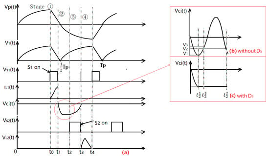
Figure 5.
The waveform of nodes of the EDSSH circuit in one cycle. (a) The nodal waveforms; (b) The of DSSH circuit without D5; (c) The of EDSSH circuit with D5.
Take a vibration period in resonance as an example to illustrate the operation process and control strategy of the circuit. (1) The first stage (Figure 4a, 0–t1 of Figure 5a): In the initial stage of system vibration, the switches S1 and S2 are turned off, and the PEH is in the vibration state without load coupling. Voltage is generated across the PEH due to structural bending. When the vibration amplitude and the voltage of the PEH () reach the maximum at t0 of the positive half period, the control circuit of S1 controls S1 turn on automatically until it detects the maximum of . The electric energy of the PEH is transferred from the Cp to L1 in one way in the Cp-L1 loop at this time. The electric energy transfer is complete when drops to near zero; at this time the control circuit of S1 turns off S1 automatically. (2) The second stage (Figure 4b, t1–t2 of Figure 5a): L1 transfers electric energy to Ci automatically due to LC oscillation. Due to the built-in diode D5 in the L1-Ci loop, the electric energy of L1 can only be transferred from L1 to Ci in one direction, and the loop does not have reverse feedback from Ci to L1 caused by multiple LC oscillations. (3) The third stage (Figure 4c, t2–t3 of Figure 5a): The control circuit of S2 controls S2 turn on when the voltage of reaches the maximum for a brief time, and S2 turns off when the current in the inductor L2 reaches the maximum. Ci transfers electric energy to L2 automatically due to LC oscillation during this time. (4) The fourth stage (Figure 4d, t3–t4 of Figure 5a): Electric energy is stored on CS of the buck-boost circuit.
3. Circuit Modeling
In the case of resonance of the PEH, suppose that the frequency of is and the period is . In time, the circuit harvests electric energy from PEH twice in a vibration cycle. For the convenience of introduction, the energy conversion relationship of the circuit in an energy extraction cycle is modeled.
3.1. The Cp-L1 Loop
The main circuit of the Cp-L1 loop. Combined with the research of Zhang [], suppose the excitation signal is , where and are the amplitude and frequency of the signal, respectively. The end displacement of the piezoelectric beam structure is , where is the amplitude of the displacement signal and is the phase angle between . In the case of without circuit coupling, the voltage across the PEH is , where is the voltage across the PEH when it reaches the extreme value of displacement, χ is the electromechanical coupling coefficient and is the piezoelectric clamping capacitance. There is an energy transfer in half a vibration period, and the electric energy generated by the PEH is . Electric energy consumed by the rectifier bridge in this period is , where is the forward voltage drop of a diode.
Regarding the power consumption of the control circuit of S1, the control circuit of S1 is dormant most of the time and does not consume electric energy. It only works for a very short time () when reaches the peak. The is equal to 1/4 of the period () of the LC oscillation circuit composed of CP and L1. The power loss of the control circuit of S1 consists of four parts: (1) The power loss of input terminal of TSX339 () is mainly the electric energy consumption on resistor R1 and R2. The maximum power supply of TSX 339 is 18 V, the maximum input voltage is 16 V, the typical value of input resistance is and the typical value of the current at the forward input terminal and reverse input terminal is . Therefore, the input terminal electrical power consumption of TSX339 is . (2) The power loss of output terminal of TSX339 () is mainly the electric energy consumption on resistor R3 and R4. Since the gating voltage of IRF5852 is 5.5 V and the voltage amplitude of is 12.26 V, the resistance of variable resistor R3 was set as 2.46 . At this time the current flowing through R3 and R4 is , and the power loss is . (3) The power consumption of TSX339 itself (): According to the electrical characteristics of TSX339, the typical current of its single comparator is 5µA, so the consumed electric energy is . (4) The power loss on IRF5852 (): The typical on-resistance of IRF5852 is 0.09 , so the power loss on IRF5852 is . Thus, the power consumption of the control circuit of S1 is .
Let the energy conversion coefficient of Cp-L1 circuit loop be , then the electric energy transferred to the inductor L1 at this time is:
3.2. The L1-Ci Circuit
Only one charge occurs on Ci in a half cycle due to the influence of reverse feedback blocking-up caused by diode D5. Assuming that the capacitance value of Ci is , the initial voltage value of Ci is , and the voltage increase value of Ci after charging is because the positive pole of the negative capacitance Ci is grounded, so , and , and the increased value of electric energy of Ci after the charging is completed is:
The charging current only flows through the diode D5 once in half a cycle, so the energy consumed by the diode D5 in this process is , where a and b are the starting and ending time of charging of capacitor Ci, respectively. Assume that the efficiency of electric energy transfer of the loop is . According to the law of conservation of energy, we can obtain , and it can also be expressed in this way:
By solving Equation (3), we can obtain as follows:
It can be seen from Formula (4) that is only related to when parameters of the circuit are determined because is only related to , and is only related to . According to Tang [], the expression of is as follows:
where, and are the modal mass, modal stiffness and modal damping ratio of the PEH, respectively. By substituting Formulas (4) and (5) into Formula (2), we can obtain .
3.3. The Ci-L2 Loop
Regarding the power consumption of the control circuit of S2, the control circuit of S2 is dormant most of the time and does not consume electric energy. It only works for a very short time () when reaches the peak. The is equal to 1/4 of the period () of the LC oscillation circuit composed of Ci and L2. The power loss of the control circuit of S2 consists of four parts: (1) The power loss of the input terminal of MAX9064 () is mainly the electric energy consumption on resistors R5, R6 and R7. The maximum voltage of is 13.87 V. The input voltage range of MAX9064 is 0 to 5.5 V. In order to make the supply voltage and forward input voltage of MAX9064 reach 5.5 and 0.2 V, respectively, when reaches 13.87 V, the resistance of R5, R6 and R7 was set as respectively. At this time the current flowing through R3 and R4 is . Therefore, the input terminal electrical power consumption of MAX9064 is . (2) The power loss of output terminal of MAX9064 () is mainly the electric energy consumption on resistors R8, R9 and R10. To ensure that the electric energy of Ci is just transferred to L2, the conduction time of switch S2 must be just equal to ; that is, the discharge time of the discharge circuit composed of C2 and R9 is equal to . According to this, R8, R9 and R10 were set as respectively. Therefore, the power loss on R8 and R9 is and , respectively, and the power loss on R10 is equal to the electric energy on C2 (). Thus, . (3) The power consumption of MAX9064 itself (): According to the electrical characteristics of MAX9064, the maximum value of operating current is 100 nA, so the consumed electric energy is . (4) The power loss on IRF5852 (): The typical on-resistance of IRF5852 is 0.09 , so the power loss on IRF5852 is
. Therefore, the power consumption of the control circuit of S1 is .
Assuming that the residual electric energy of Ci is zero when the energy transfer is completed, since there is only one discharge process on Ci during this time, the electric energy consumed on D6 is:
Suppose that the efficiency of electric energy transfer of the circuit is , then the electric energy transferred to L2 is:
3.4. The Buck-Boost Circuit
Let the capacitance, the initial voltage and the increased voltage after a single energy conversion of CS be , and , respectively. Suppose that the power transfer efficiency of the circuit is , then according to the law of conservation of energy, we have , and it can also be expressed as:
By solving Formula (8), we can obtain as follows:
We can obtain by substituting Formula (7) into Formula (9). Then the electric energy increment on the charging capacitor Cs can be obtained as follows:
According to the discussion above, the models of key parameters reflecting circuit performance are summarized as follows:
- Voltage on CS (charging voltage of the circuit)
- 2.
- Electrical power of CS (electric energy harvesting power of the circuit)
- 3.
- Power Budget
The calculation formula of average power is During an energy extraction cycle with a duration of , the electric power generated by the piezoelectric vibrator is:
The electric power losses of D1–D7, R1–R10, TSX339, MAX9064, Q1 and Q2 during an energy extraction cycle with a duration of are shown in Table 1.

Table 1.
Power budget.
3.5. Validation of the Mode
In order to verify the accuracy of the model, the calculation results were compared with the existing literature and simulation results using the software MULTISIM. Parameters of the circuit are shown in Table 2.

Table 2.
Parameters of the circuit.
- Comparison with the Existing Literature
Taking as the coupling factor of the PEH, the calculation results of present model were compared with Tang’s model [] in terms of the influence of excitation frequency () on amplitude voltage of the PEH () in case = 0.0015 (weak coupling), 0.015 (medium coupling) and 0.15 (strong coupling). The results are shown in Figure 6, it can be seen that the error is less than 1%. Moreover, the strongest response of the EDSSH circuit to the PEH occurs in the case of medium coupling, and the corresponding output voltage amplitude and excitation frequency are 12.26 V and 23.88 Hz, respectively.
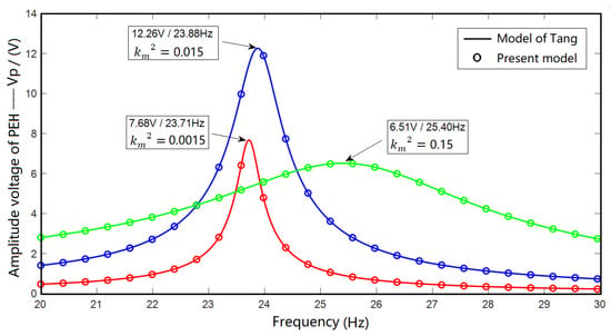
Figure 6.
Comparison of the calculation results of present model with the calculation results of existing literature in three coupling cases.
- 2.
- Comparison with the Simulation Results
The calculation results of present model were compared with the simulation results of MULTISIM in terms of the voltage across CS after charging for 60 s in three coupling cases. The results are shown in Figure 7. It can be seen that the voltage across CS () calculated by present model in three coupling cases is 1.86, 4.48 and 1.59 V, and the simulation results are 1.58, 3.86 and 1.33 V with errors of 17.72%, 16.06% and 19.55%, respectively, which shows that the present model has good prediction ability. However, the simulation result is lower than the calculation result of present model. The main reason is that the loss of energy in each circuit is not fully considered in the model, but these factors are included in the electronic component parameter model of MULTISIM.
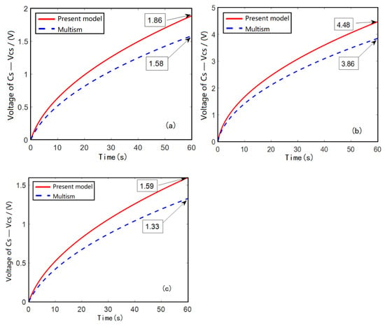
Figure 7.
Comparison of the calculation results of present model with simulation results of MULTISIM in three coupling cases; (a)= 0.0015, (b)0.015, (c)= 0.15.
4. Simulation and Experiment
4.1. Simulation of Rectifier Bridge
MULTISIM software was used to simulate the circuit (Figure 3). Figure 8 shows the waveform of the output voltage (, red curve) generated by the PEH after being excited and the waveform of the output voltage (, blue curve) of the rectifier bridge. It can be seen that the rectifier bridge rectifies the AC sinusoidal signal of into the DC signal ().
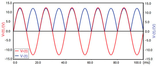
Figure 8.
Output waveforms of the PEH and the rectifier bridge.
4.2. Simulation of Control Circuit of S1
The control circuit of S1 consists of comparator TSX339, resistors R1, R2, R3 and capacitor C1. The no-inverting input voltage of TSX339 is represented by , the inverting input voltage is represented by and the output voltage is represented by . and are the same. The main function of the circuit is to automatically make the high voltage when reaches its peak value. controls the conduction of field-effect transistor Q1 (IRF5852) for a short duration at the same time. Electrical energy on CP must be transmitted to L1 in one way. The waveforms of , and are shown in Figure 9. It can be seen that is low voltage due to being lower than in the period from 0 to t0. During this period, IRF5852 is turned off. When reaches its peak value at t0, becomes higher than drain-source on-voltage of IRF5852 due to being higher than . Then IRF5852 turns on automatically because is high voltage. When decreases to drain-source on-voltage of IRF5852 near t1, IRF5852 turns off automatically.
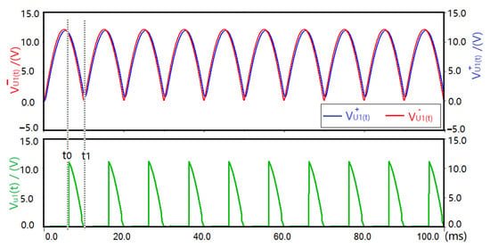
Figure 9.
Waveforms of terminals of TSX339.
4.3. Experiment
4.3.1. Experimental Platform
The experimental platform is shown in Figure 10. The function generator1 (AFG3021C) generates a sine wave function (acceleration 0.5 g) at the natural frequency of the PEH. The power amplifier amplifies the excitation signal generated by function generator1 to drive the exciter to vibrate, which makes the PEH produce resonance and output 12.26 V AC. Function generator2 simulates the control signal of switch S2. The designed circuit board (the circuit diagram is shown in Figure 3) is connected with the output terminal of the PEH to harvest the electric energy generated by the PEH. The oscilloscope (TDS2024C) is used to measure the voltage signal of the corresponding measuring point on the circuit board.
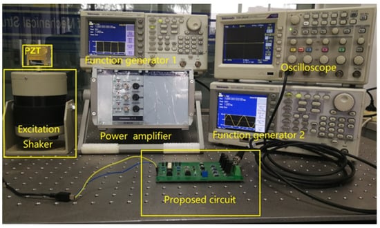
Figure 10.
Experimental scheme and platform.
4.3.2. Influence of RFBC on Electric Energy Harvesting Efficiency
In order to verify that the RFBC in the EDSSH circuit can make the circuit maintain the optimal electric energy harvesting efficiency, taking the L1-Ci circuit as an example, the output voltage waveform of capacitor Ci was measured in one energy harvesting cycle (0.01 s) when DSSH circuit was not configured with D5 (Figure 11a) and EDSSH circuit was configured with D5 (Figure 11b).
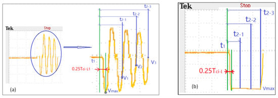
Figure 11.
The waveform of in two cases: (a) without D5 in DSSH circuit (b) with D5 in EDSSH circuit.
It can be seen that can reach the optimal value (Vmax = −13.84 V) only when the duration of t1-t2 is equal to one fourth of the oscillation period (0.25∗Tci-L1) of the L1-Ci loop precisely. Otherwise, due to LC oscillation, the voltage values for Ci are different at different times of t2. For example, the voltages of t2 at , and are V1 (−7.86 V), V2 (−3.74 V) and V3 (−0.42 V), which are 56.79%, 26.98% and 3.03% of the optimal value (Vmax), respectively. That is to say, the efficiency of energy transferring of L1-Ci loop of DSSH circuit without D5 cannot be kept at the optimal value. Figure 11b is the waveform of the output voltage of the capacitor Ci when the EDSSH circuit is configured with D5. It can be seen that only if the duration of t1-t2 is more than one fourth of the oscillation period of L1-Ci loop, the L1-Ci circuit only has one-way power transfer from L1 to Ci; that is, after L1 charges Ci, the voltage of Ci keeps the optimal value (Vmax) unchanged.
4.3.3. Efficiency of EDSSH Circuit
The voltage of the PEH and the increased voltage of Ci were measured with the experimental platform shown in Figure 10, and their amplitudes are and , respectively. The electric energy consumed by diode D7 is . It can be seen from Equation (9) that the value of in each charging cycle is related to the voltage of capacitor (CS) and the charging time (). Thus, is not a constant but a variable related to and . The of CS was measured after 60 s charging, and the results are shown in Table 3, where is the efficiency of the circuit from the PEH to Ci, is the charging efficiency within 60 s of the circuit from D6 to Cs, is the total electric energy accumulated on Ci within 60 s charging time and is the total efficiency of the circuit.

Table 3.
Efficiency and nodal-voltage of EDSSH circuit.
4.3.4. Efficiency Comparison between EDSSH and DSSH Circuits
It can be seen from Figure 11 that the output voltage of the DSSH circuit is uncertain. The voltage of CS of EDSSH and DSSH circuits was measured after 60 s charging time five times, and the charging efficiency of each time was calculated, taking the average value. The results are shown in Table 4, where and are the average charging efficiency of EDSSH and DSSH circuits, respectively. It can be seen that the average charging efficiency of the EDSSH circuit is 1.51 times than that of DSSH.

Table 4.
Efficiency comparison between EDSSH circuit and DSSH circuit.
5. Discussion
5.1. Advantages of EDSSH Circuit
- (1)
- The low-power design. The complex control module and special power module in the DSSH circuit are required. Compared with the control circuit of S1 and S2 in the DSSH circuit, the EDSSH circuit integrated a module of a control circuit of switch S1 and S2 with simple structure and low-power IC. The control circuit of S1 only comprises a comparator TSX339, three resistors and one capacitor. The maximum average power consumption of TSX339 is 0.96 μW in one electrical energy extraction cycle when reaches the maximum value of 12.26 V. In addition, the power supply and input signal of the comparator TSX339 are from the output terminal rectifier V1. The control circuit of S2 only comprises a comparator MAX9064, four resistors and one capacitor. The maximum average power consumption of MAX9064 is lower than 1 μW in one electrical energy extraction cycle when reaches the maximum value. In addition, the power supply and input signal of the comparator MAX9064 are from the . According to Section 4.3, the total average charging efficiency of the EDSSH circuit is 52.16% compared with 34.55% of that of the DSSH circuit.
- (2)
- The high-efficiency design. The RFBC is used to keep the power harvesting efficiency at the optimal value. Diodes D5 and D6 are configured in the loop to avoid reverse feedback of electric energy caused by LC oscillations in one energy harvesting cycle. Taking the L1-Ci circuit as an example, if D5 is not configured in the DSSH circuit, the duration of t1-t2 should be precisely controlled to be equal to one fourth of the oscillation period of L1-Ci. Otherwise, the voltage values of Ci are different according to different time of t2 (Figure 5b, the voltage on Ci at , and are V1, V2 and V3, respectively), and the efficiency of electric energy transfer is uncertain. When the EDSSH circuit is configured with D5, as long as the duration of t1-t2 is greater than one fourth of the oscillation period of L1-Ci, the L1-Ci loop only has one-way power transfer from L1 to Ci; that is, the voltage of Ci remains unchanged after L1 charging Ci (Figure 5c) so as to maintain the optimal efficiency.
- (3)
- The adaptive design. Firstly, the control circuit of S1 is in the sleep state most of the time and self-cold-starting and turns on for a short time when reaches its peak value. The control circuit of S2 is in the sleep state most of the time and self-cold-starting and turns on for a short time when reaches its peak value. Secondly, it can adapt to the wide frequency range of input sinusoidal voltage signal. The main reason is that the single energy acquisition time of the circuit is only 1.6004 ms (including 0.0124 ms of CP-L1 loop, 0.0086 ms of L1-Ci- loop, 0.0086 ms of Ci-L2 loop and 1.5708 ms of L2-Cs- loop). As long as half of the cycle of the input sinusoidal voltage signal is longer than , the acquisition process can be completed automatically. Therefore, the circuit can automatically adapt to the input sinusoidal voltage signal of 1~312.5 Hz. Lastly, the circuit features a buck-boost structure, which can automatically match various loads.
5.2. Comparison of Charging Performance between EDSSH Circuit and DSSH Circuit
Because of the RFBC, the power conversion efficiency of the L1-Ci loop and Ci-L2 loop in the EDSSH circuit can be stabilized at the optimal value. The DSSH circuit, because it does not use this technology, exhibits loop reverse feedback, resulting in the reduction of power transfer efficiency. Here, we can compare the charging performance between the EDSSH circuit and DSSH circuit by using the established model (Formula (12) in this paper) and MULTISIM software. For example, the power transfer efficiency corresponding to and in Figure 5a is 0.8 and 0.6. Set 1 mF, 0.015 and analyze the voltage of charging capacitor () after 60 s charging time under three conditions of = 1.0, 0.8 and 0.6. The results are shown in Figure 12a, and it can be seen that increases with the increase in .The influence of the normalization efficiency (()) of on the normalized power ()) was analyzed. The results are shown in Figure 12b, and it can be seen that increases with the increase in . Similar to , the influence of on and the influence of the normalization efficiency ()) of on the normalized power ()) are shown in Figure 12c,d, respectively. The results show that increases with the increase in and increases with the increase in . This proves that the RFBC technology can significantly improve the amplitude of output voltage and keep the efficiency of each circuit at the optimal value.
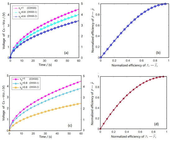
Figure 12.
Comparison of charging performance of the two circuits. (a) Influence of D5 on the charging voltage of two circuits. (b) Influence of normalized efficiency of L1-Ci loop on normalized power. (c) Influence of D6 on the charging voltage of two circuits. (d) Influence of normalized efficiency of Ci-L2 loop on normalized power.
5.3. Influence of Capacitance of Cs on Charging Performance
The influence of capacitance of Cs on charging performance was analyzed based on the proposed circuit model (Formula (12)) and MULTISIM software. In the process of electric energy harvesting, the influence of the capacitance of Cs on its charging voltage is shown in Figure 13. It can be seen that when the capacitance and , reaches 14.76, 4.48 and 1.26 V, respectively, after 60 s charging time. This indicates that the voltage on the charging capacitor increases faster with smaller capacitor .
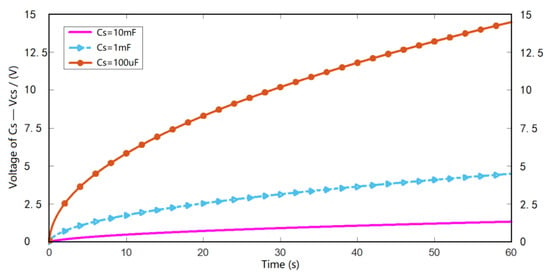
Figure 13.
Influence of capacitance on ).
5.4. Influence of Initial Voltage of Cs on Charging Performance
In the process of power harvesting, the initial capacitance of Cs () has a significantly influence on the increment of voltage () and voltage value () of the charging capacitor. Influence of initial voltage of Cs on charging performance can also be analyzed based on the proposed circuit model (Formula (12)) and MULTISIM software. As can be seen from Figure 14, when is 0, 5 and 10 V, reaches 4.48, 5.16 and 6.75 V, respectively, after 60 s charging time. Figure 15 shows that when increases from 0 to 10 V, the voltage increase value of charging capacitor decreases from 4.48 to 1.75 V after 60 s charging time.
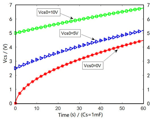
Figure 14.
Influence of on .
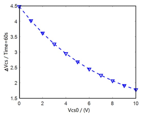
Figure 15.
Influence of on .
5.5. Design Criteria for Parameters of EDSSH Circuit
Assuming that the piezoelectric structure resonates under the frequency of 50 Hz (period = 0.02 s), the longest time interval (t0–t3) between two power acquisitions is half of the resonance period () according to Figure 5; that is to say, all the links of piezoelectric electric energy transfer to Cs are completed in this . Since the time required for each link is related to parameters of the circuit, it is necessary to discuss the design criteria of the circuit’s parameters of , , , , and control modules of S1 which are related to power transfer efficiency.
1. Design of parameters of main circuit components: First, the clamping capacitor () of the piezoelectric structure was determined after the size design. In order to transfer the electric energy of CP to L1 to the greatest extent, the time (t0-t1) of electric energy transferred from the capacitor CP to the inductor L1 should be controlled at one eighth of ; that is, the oscillation period of Cp-L1 loop should be less than . According to the calculation formula of the LC oscillation period, the design range of is . Then, the charging capacitor was selected according to the actual needs. Since the oscillation period of the L2-CS loop is generally less than , it is assumed that the capacitance value of the charging capacitor is , and the design range of can be determined by . Finally, the oscillation period of the L1-Ci circuit is less than , so . Of course, this is the basic principle and order. On the premise that the total time to complete a power transfer is less than , the time length of each circuit can be adjusted, and then the values of , , and can be determined.
2. Parameter design of switch control circuit of S1: First, the power consumption of the circuit should be as small as possible; that is to say, the resistance value of and should be as large as possible. Then the delay time () of the RC delay circuit composed of C1 and R2 should be controlled to be as short as possible, so that the power transfer can start at the amplitude of . The values of R2 and C1 were determined by = . Finally, the comparator should choose the components with the lowest power consumption.
6. Conclusions
- (1)
- A low-power high-efficiency adaptive electric energy harvesting circuit for broadband PEHs is proposed. The control circuit of switches is simpler, the electronic components used is fewer, and the power loss of switch control circuits is less than that of the DSSH circuit. It is self-cold-starting with a threshold voltage as low as 0.2 V.
- (2)
- Compared with the DSSH circuit, the electric energy harvesting efficiency of the EDSSH circuit with the proposed RFBC is stable at the optimal value. The average charging efficiency of the EDSSH circuit is 1.51 times than that of DSSH.
- (3)
- During the circuit test, the input voltage is an ideal sine wave signal, so the circuit can successfully capture the power extreme point of the signal. If there is noise interference in the input voltage, the circuit may operate incorrectly when capturing the power extreme point, which affects the power extraction efficiency of the circuit. Therefore, it is necessary to add circuit modules at the input of the circuit to remove noise interference.
- (4)
- According to the electric energy conversion time of each circuit of the circuit and the charging time of CS, it can be calculated that the frequency range of the input voltage signal that the circuit can match is 1–312.5 Hz To broaden the frequency range of the input signal that the circuit can match, the relevant components must be recalculated and replaced.
- (5)
- The performance of the circuit matching nonlinear piezoelectric vibration energy harvester needs to be further investigated.
Author Contributions
A.Z. was the supervisor providing funding and administrating the project; wrote, reviewed and edited the manuscript and carried out the investigation, methodology, analysis, and validation. X.H. made great contributions to the application of MATLAB in simulation. Z.L. helped to test the parameters and also helped to perform some verification experiments. All authors have read and agreed to the published version of the manuscript.
Funding
This research was funded by Guangxi Natural Science Foundation Program 2018JJA160218, the National Natural Science Foundation of China under grants 51965014, 51765014.
Conflicts of Interest
The authors declare no conflict of interest.
References
- Whelan, M.; Salas Zamudio, N.; Kernicky, T. Structural identification of a tied arch bridge using parallel genetic algorithms and ambient vibration monitoring with a wireless sensor network. J. Civ. Struct. Health Monit. 2018, 8, 1–16. [Google Scholar] [CrossRef]
- Muduli, L.; Mishra, D.P.; Jana, P. Application of wireless sensor network for environmental monitoring in underground coal mines: A systematic review. J. Netw. Comput. Appl. 2018, 106, 48–67. [Google Scholar] [CrossRef]
- Trasviña Moreno, C.; Blasco, R.; Marco, Á.; Casas, R.; Trasviña-Castro, A. Unmanned aerial vehicle based wireless sensor network for marine-coastal environment monitoring. Sensors 2017, 17, 460. [Google Scholar] [CrossRef]
- Peng, X.; Wen, Y.; Li, P.; Yang, A.; Bai, X. A wideband acoustic energy harvester using a three degree-of-freedom architecture. Appl. Phys. Lett. 2013, 103, 164106. [Google Scholar] [CrossRef]
- Selvan, K.V.; Ali, M.M. Micro-scale energy harvesting devices: Review of methodological performances in the last decade. Renew. Sustain. Energy Rev. 2016, 54, 1035–1047. [Google Scholar] [CrossRef]
- Elahi, H.; Eugeni, M.; Gaudenzi, P. A review on mechanisms for piezoelectric-based energy harvesters. Energies 2018, 11, 1850. [Google Scholar] [CrossRef] [Green Version]
- Safaei, M.; Sodano, H.A.; Anton, S.R. A review of energy harvesting using piezoelectric materials: State-of-the-art a decade later (2008–2018). Smart Mater. Struct. 2019, 28, 113001. [Google Scholar] [CrossRef]
- Erturk, A.; Inman, D.J. A distributed parameter electromechanical model for cantilevered piezoelectric energy harvesters. J. Vib. Acoust. 2008, 130, 1257–1261. [Google Scholar] [CrossRef]
- Erturk, A.; Inman, D.J. Issues in mathematical modeling of piezoelectric energy harvesters. Smart Mater. Struct. 2008, 17, 065016. [Google Scholar] [CrossRef] [Green Version]
- Liao, Y.; Sodano, H.A. Model of a single mode energy harvester and properties for optimal power generation. Smart Mater. Struct. 2008, 17, 065026. [Google Scholar] [CrossRef]
- Liao, Y.; Sodano, H.A. Optimal parameters and power characteristics of piezoelectric energy harvesters with an RC circuit. Smart Mater. Struct. 2009, 18, 045011. [Google Scholar] [CrossRef]
- Fakharian, O.; Salmani, H.; Kordkheili, S. A lumped parameter model for exponentially tapered piezoelectric beam in transverse vibration. J. Mech. Sci. Technol. 2019, 33, 2043–2048. [Google Scholar] [CrossRef]
- Kärki, S.; Lekkala, J. A lumped-parameter transducer model for piezoelectric and ferroelectret polymers. Measurement 2012, 45, 453–458. [Google Scholar] [CrossRef]
- Baishya, S.; Borthakur, D.; Kashyap, R.; Chatterjee, A. A high precision lumped parameter model for piezoelectric energy harvesters. IEEE Sens. J. 2017, 17, 8350–8355. [Google Scholar] [CrossRef]
- Wang, G.Q.; Lu, Y.M. An improved lumped parameter model for a piezoelectric energy harvester in transverse vibration. Shock. Vib. 2014, 2014 Pt 1, 1–12. [Google Scholar] [CrossRef] [Green Version]
- Sriramdas, R.; Pratap, R. An experimentally validated lumped circuit model for piezoelectric and electrodynamic hybrid harvesters. IEEE Sens. J. 2018, 18, 2377–2384. [Google Scholar] [CrossRef]
- Ruderman, M.; Kamiya, Y.; Iwasaki, M. Extended lumped parameter electromechanical model of piezoelectric actuators. In Proceedings of the 2015 IEEE International Conference on Mechatronics (ICM), Nagoya, Japan, 6–8 March 2015; pp. 290–295. [Google Scholar]
- Elvin, N.G.; Elvin, A.A. A general equivalent circuit model for piezoelectric generators. J. Intell. Mater. Syst. Struct. 2019, 20, 3–9. [Google Scholar] [CrossRef]
- Elvin, N.G.; Elvin, A.A. A coupled finite element-circuit Simulation model for analyzing piezoelectric energy generator. J. Intell. Mater. Syst. Struct. 2009, 20, 587–595. [Google Scholar] [CrossRef]
- Roundy, S.; Leland, E.S.; Baker, J.; Carleton, E.; Reilly, E.; Lai, E.; Otis, B.; Rabaey, J.M.; Wright, P.K.; Sundararajan, V. Improving power output for vibration-based energy scavengers. IEEE Pervasive Comput. 2005, 4, 28–36. [Google Scholar] [CrossRef]
- Yang, Y.; Tang, L. Equivalent circuit modeling of piezoelectric energy harvesters. J. Intell. Mater. Syst. Struct. 2009, 20, 2223–2235. [Google Scholar] [CrossRef]
- Wang, G.; Chen, G.; Bai, F. modeling and identification of asymmetric Bouc-Wen hysteresis for piezoelectric actuator via a novel differential evolution algorithm. Sens. Actuators A Phys. 2015, 235, 105–118. [Google Scholar] [CrossRef]
- Zhang, J.; Xia, P. An improved PSO algorithm for parameter identification of nonlinear dynamic hysteretic models. J. Sound Vib. 2017, 389, 153–167. [Google Scholar] [CrossRef]
- Ko, Y.R.; Hwang, Y.; Chae, M.; Kim, T.H. Direct identification of generalized Prandtl-Ishlinskii model inversion for asymmetric hysteresis compensation. ISA Trans. 2017, 70, 209–218. [Google Scholar] [CrossRef]
- Saleem, A.; Al-Ratrout, S.; Mesbah, M. A fitness function for parameters identification of Bouc-Wen hysteresis model for piezoelectric actuators. In Proceedings of the International Conference on Electrical and Electronic Engineering (ICEEE), Istanbul, Turkey, 3–5 May 2018; pp. 119–123. [Google Scholar]
- Noël, J.P.; Esfahani, A.F.; Kerschen, G.; Schoukens, J. A nonlinear state-space approach to hysteresis identification. Mech. Syst. Signal Process. 2017, 84, 171–184. [Google Scholar] [CrossRef] [Green Version]
- He, C.; Zhi, W.; Liu, X. Magnetic property parameter identification of steel pole based on GA-PSO hybrid algorithm. Chin. J. Sci. Instrum. 2017, 38, 838–843. [Google Scholar]
- Wang, R.; Zhang, X. Parameters optimization and experiment of a planar parallel 3-dof nanopositioning system. IEEE Trans. Ind. Electron. 2018, 65, 2388–2397. [Google Scholar] [CrossRef]
- Xie, S.L.; Liu, H.T.; Mei, J.P.; Gu, G.Y. Modeling and compensation of asymmetric hysteresis for pneumatic artificial muscles with a modified generalized Prandtl-Ishlinskii model. Mechatronics 2018, 52, 49–57. [Google Scholar] [CrossRef]
- Billings, S.A. Nonlinear System Identification: NARMAX Methods in the Time, Frequency, and Spatio-Temporal Domains; John Wiley & Sons: Hoboken, NJ, USA, 2013. [Google Scholar]
- Eichhorn, C.; Goldschmidtboeing, F.; Woias, P. Bidirectional frequency tuning of a piezoelectric energy converter based on a cantilever beam. J. Micromech. Microeng. 2009, 19, 1693–1696. [Google Scholar] [CrossRef]
- Li, W.G.; He, S.; Yu, S. Improving power density of a cantilever piezoelectric power harvester through a curved L-Shaped proof mass. IEEE Trans. Ind. Electron. 2010, 57, 868–876. [Google Scholar] [CrossRef]
- Shen, D.; Park, J.H.; Ajitsaria, J. The design, fabrication and evaluation of a MEMS PZT cantilever with an integrated Si proof mass for vibration energy harvesting. J. Micromech. Microeng. 2008, 18, 055017. [Google Scholar] [CrossRef]
- Morris, D.J.; Youngsman, J.M.; Anderson, M.J. A resonant frequency tunable, extensional mode piezoelectric vibration harvesting mechanism. Smart Mater. Struct. 2008, 17, 065021. [Google Scholar] [CrossRef]
- Guan, Q.C.; Ju, B.; Xu, J.W.; Liu, Y.B.; Feng, Z.H. Improved strain distribution of cantilever piezoelectric energy harvesting devices using H-shaped proof masses. J. Intell. Mater. Syst. Struct. 2013, 24, 1059–1066. [Google Scholar] [CrossRef]
- Huang, D.; Zhou, S.; Litak, G. Theoretical analysis of multi-stable energy harvesters with high-order stiffness terms. Commun. Nonlinear Sci. Numer. Simul. 2019, 69, 270–286. [Google Scholar] [CrossRef]
- Yuan, T.C.; Yang, J.; Chen, L.Q. A harmonic balance approach with alternating frequency/time domain progress for piezoelectric mechanical systems. Mech. Syst. Signal Process. 2019, 120, 274–289. [Google Scholar] [CrossRef]
- Wang, C.; Zhang, Q.; Wang, W. Low-frequency wideband vibration energy harvesting by using frequency up-conversion and quin-stable nonlinearity. J. Sound Vib. 2017, 399, 169–181. [Google Scholar] [CrossRef]
- Fan, K.; Tan, Q.; Liu, H. Improved energy harvesting from low-frequency small vibrations through a monostable piezoelectric energy harvester. Mech. Syst. Signal Process. 2019, 117, 594–608. [Google Scholar] [CrossRef]
- Nabavi, S.; Zhang, L. Nonlinear multi-mode wideband piezoelectric MEMS vibration energy harvester. IEEE Sens. J. 2019, 19, 4837–4848. [Google Scholar] [CrossRef]
- Wang, Y.J.; Chuang, T.Y.; Lee, C. Resonant frequency self-tunable piezoelectric cantilevers for energy harvesting and disturbing torque absorbing. Sens. Actuators A Phys. 2019, 285, 25–34. [Google Scholar] [CrossRef]
- Wang, J.; Zhou, S.; Zhang, Z. High-performance piezoelectric wind energy harvester with Y-shaped attachments. Energy Convers. Manag. 2018, 181, 645–652. [Google Scholar] [CrossRef]
- Wu, Z.; Xu, Q. Design and testing of a novel bidirectional energy harvester with single piezoelectric stack. Mech. Syst. Signal Process. 2019, 122, 139–151. [Google Scholar] [CrossRef]
- Hu, Y.; Yong, X. A wideband vibration energy harvester based on a folded asymmetric gapped cantilever. Appl. Phys. Lett. 2014, 104, 329. [Google Scholar] [CrossRef]
- Gael, S.; Hiroki, K.; Daniel, G.; Benjamin, D. Experimental duffing oscillator for broadband piezoelectric energy harvesting. Smart Mater. Struct. 2011, 20, 102001. [Google Scholar]
- Kim, I.H.; Jung, H.J.; Bo, M.L. Broadband energy-harvesting using a two degree-of-freedom vibrating body. Appl. Phys. Lett. 2011, 98, 987. [Google Scholar] [CrossRef]
- Abdelkefi, A.; Najar, F.; Nayfeh, A.H. An energy harvester using piezoelectric cantilever beams undergoing coupled bending–torsion vibrations. Smart Mater. Struct. 2011, 20, 115007. [Google Scholar] [CrossRef]
- Hajati, A.; Kim, S.G. Ultra-wide bandwidth piezoelectric energy harvesting. Appl. Phys. Lett. 2011, 99, 175–252. [Google Scholar] [CrossRef] [Green Version]
- Karami, M.A.; Inman, D.J. Parametric study of zigzag microstructure for vibrational energy harvesting. J. Microelectromechan. Syst. 2012, 21, 145–160. [Google Scholar] [CrossRef]
- Fan, K.; Chang, J.; Pedrycz, W. A nonlinear piezoelectric energy harvester for various mechanical motions. Appl. Phys. Lett. 2015, 106, 094102. [Google Scholar] [CrossRef]
- Hu, H.; Dai, L.; Chen, H.; Jiang, S.; Wang, H.; Laude, V. Two methods to broaden the bandwidth of a nonlinear piezoelectric bimorph power harvester. J. Vib. Acoust. 2017, 139, 031008. [Google Scholar] [CrossRef]
- Rui, X.; Li, Y.; Liu, Y. Experimental study and parameter optimization of a magnetic coupled piezoelectric energy harvester. Appl. Sci. 2018, 8, 2609. [Google Scholar] [CrossRef] [Green Version]
- Bo, Z.; Yu, J.; Elmaimouni, L. Magneto-electric effect on guided waves in functionally graded piezoelectric–piezomagnetic fan-shaped cylindrical structures. Materials 2018, 11, 2174. [Google Scholar]
- Dong, W.; Shilong, S.; Tse, P.W. A general sequential Monte Carlo method based optimal wavelet filter: A Bayesian approach for extracting bearing fault features. Mech. Syst. Signal Process. 2015, 52–53, 293–308. [Google Scholar]
- Alcala-Jimenez, L.R.; Jensen, T.P.; Lei, A. Increased mechanical robustness of piezoelectric magnetoelastic vibrational energy harvesters-ScienceDirect. Microelectron. Eng. 2019, 207, 19–26. [Google Scholar] [CrossRef]
- Valerio, A.; Carmine, S.C.; Daniele, D.; Damiano, L.; Ciro, V. Magneto-mechanical optimization and analysis of a magnetostrictive cantilever beam for energy harvesting-ScienceDirect. J. Magn. Magn. Mater. 2019, 475, 401–407. [Google Scholar]
- Zhao, L.; Conlon, S.C.; Semperlotti, F. Broadband energy harvesting using acoustic black hole structural tailoring. Smart Mater. Struct. 2014, 23, 065021. [Google Scholar] [CrossRef]
- Leadenham, S.; Erturk, A. Nonlinear M-shaped broadband piezoelectric energy harvester for very low base accelerations: Primary and secondary resonances. Smart Mater. Struct. 2015, 24, 055021. [Google Scholar] [CrossRef] [Green Version]
- Harne, R.L.; Sun, A.; Wang, K.W. Leveraging nonlinear saturation-based phenomena in an L-shaped vibration energy harvesting system. J. Sound Vib. 2015, 363, 517–531. [Google Scholar] [CrossRef]
- Qin, Y.; Wei, T.; Zhao, Y. Simulation and experiment on bridge-shaped nonlinear piezoelectric vibration energy harvester. Smart Mater. Struct. 2018, 28, 045015. [Google Scholar] [CrossRef]
- Shi, G.; Xia, Y.; Wang, X.; Qian, L.; Ye, Y.; Li, Q. An efficient self-powered piezoelectric energy harvesting CMOS interface circuit based on synchronous charge extraction technique. Circuits Syst. I Regul. Pap. IEEE Trans. 2018, 65, 804–817. [Google Scholar] [CrossRef]
- Shaikh, F.; Zeadally, S. Energy harvesting in wireless sensor networks: A comprehensive review. Renew. Sust. Energ. Rev. 2016, 55, 1041–1054. [Google Scholar] [CrossRef]
- Lefeuvre, E.; Audigier, D.; Richard, C.; Guyomar, D. Buck-boost converter for sensorless power optimization of piezoelectric energy harvester. IEEE Trans. Power Electron. 2007, 22, 2018–2025. [Google Scholar] [CrossRef]
- Garbuio, L.; Lallart, M.; Guyomar, D.; Richard, C. Mechanical energy harvester with ultralow threshold rectification based on SSHI nonlinear technique. IEEE Trans. Ind. Electron. 2009, 56, 1048–1056. [Google Scholar] [CrossRef]
- Guyomar, D.; Jayet, Y.; Petit, L.; Lefeuvre, E.; Richard, C.; Lallart, M. Synchronized switch harvesting applied to self powered smart systems: Piezoactive microgenerators for autonomous wireless transmitters. Sens. Actuators A Phys. 2007, 138, 151–160. [Google Scholar] [CrossRef]
- Guyomar, D.; Badel, A.; Lefeuvre, E.; Richard, C. Towards energy harvesting using active materials and conversion improvement by nonlinear processing. Ultrason. Ferroelectr. Freq. Control IEEE Trans. 2005, 52, 584–595. [Google Scholar] [CrossRef] [Green Version]
- Liang, J.; Liao, W.H. Impedance modeling and analysis for piezoelectric energy harvesting systems. IEEE/ASME Trans. Mechatron. 2012, 17, 1145–1157. [Google Scholar] [CrossRef]
- Badel, A.; Guyomar, D.; Lefeuvre, E.; Richard, C. Piezoelectric energy harvesting using a synchronized Switch technique. J. Intell. Mater. Syst. Struct. 2006, 17, 831–839. [Google Scholar] [CrossRef]
- Shu, Y.; Lien, L.; Wu, W. An improved analysis of the SSHI interface in piezoelectric energy harvesting. Smart Mater. Struct. 2007, 16, 2253–2264. [Google Scholar] [CrossRef]
- Ramadass, Y.K.; Chandrakasan, A.P. An Efficient Piezoelectric Energy Harvesting Interface Circuit Using a Bias-Flip Rectifier and Shared Inductor. IEEE J. Solid-State Circuits 2010, 45, 189–204. [Google Scholar] [CrossRef] [Green Version]
- Lefeuvre, E.; Badel, A.; Richard, C.; Petit, L.; Guyomar, D. A comparison between several vibration-powered piezoelectric generators for standalone systems. Sens. Actuators A-Phys. 2006, 126, 405–416. [Google Scholar] [CrossRef]
- Lallart, M.; Garbuio, L.; Petit, L.; Richard, C.; Guyomar, D. Double synchronized switch harvesting (DSSH): A new energy harvesting scheme for efficient energy extraction. IEEE Trans. Ultrason. Ferroelectr. Freq. Control 2008, 55, 2119–2130. [Google Scholar] [CrossRef]
- Lefeuvre, E.; Risquez, S.; Wei, J.; Woytasik, M.; Parrain, F. Self-Biased Inductor-Less Interface Circuit for Electret-Free Electrostatic Energy Harvesters. J. Phys. Conf. Ser. Power MEMS 2014, 557, 012052. [Google Scholar] [CrossRef] [Green Version]
- Gasnier, P.; Willemin, J.; Boisseau, S.; Despesse, G.; Condemine, C.; Gouvernet, G.; Chaillout, J.-J. An autonomous piezoelectric energy harvesting IC based on a synchronous multi-Shot technique. IEEE J. Solid-State Circuits 2014, 49, 1561–1570. [Google Scholar] [CrossRef]
- Dini, M.; Romani, A.; Filippi, M.; Tartagni, M. A nanopower synchronous charge extractor IC for low-voltage piezoelectric energy harvesting with residual charge inversion. IEEE Trans. Power Electron. 2016, 31, 1263–1274. [Google Scholar] [CrossRef]
- Yeatman, E.M.; Ahmadian, M.; Ghasemi-Nejhad, M.N. Energy harvesting: Small scale energy production from ambient sources. Int. Soc. Opt. Photonics 2009, 7288, 728802. [Google Scholar]
- Shen, H.; Qiu, J.H.; Ji, H.L. Enhanced synchronized switch harvesting (ESSH): A new energy harvesting scheme for efficient energy extraction. Smart Mater. Struct. 2010, 19, 115017. [Google Scholar] [CrossRef]
- Lefeuvre, E.; Badel, A.; Richard, C.; Guyomar, D. Piezoelectric energy harvesting device optimization by synchronous electric charge extraction. J. Intell. Mater. Syst. Struct. 2005, 16, 865–876. [Google Scholar] [CrossRef]
- Wang, G.; Li, P.; Wen, L.; Ji, X. Self-powered ultra-low-power low-threshold synchronous circuit for weak piezoelectric energy harvesting. Sens. Actuators A-Phys. 2021, 322, 112632. [Google Scholar] [CrossRef]
- Wu, L.; Zhu, P.; Xie, M. A Self-powered hybrid SSHI circuit with a wide operation range for piezoelectric energy harvesting. Sensors 2021, 21, 615. [Google Scholar] [CrossRef] [PubMed]
- Din, A.U.; Kamran, M.; Mahmood, W.; Aurangzeb, K.; Lee, J.W. An efficient CMOS dual switch rectifier for piezoelectric energy-harvesting circuits. Electronics 2019, 8, 66. [Google Scholar] [CrossRef] [Green Version]
- Chen, N.; Wei, T.; Jung, H.J.; Lee, S. Quick self-start and minimum power-loss management circuit for impact-type micro wind piezoelectric energy harvesters. Sens. Actuators A-Phys. 2017, 263, 23–29. [Google Scholar] [CrossRef]
- Lallart, M. Nonlinear technique and self-powered circuit for efficient piezoelectric energy harvesting under unloaded cases. Energy Convers. Manag. 2016, 133, 444–457. [Google Scholar] [CrossRef]
- Zhang, Z.; Xiang, H.; Tang, L. Modeling analysis and comparison of four charging interface circuits for piezoelectric energy harvesting. Mech. Syst. Signal Process. 2021, 152, 107476. [Google Scholar] [CrossRef]
- Tang, L.H.; Yang, Y.W. Analysis of synchronized charge extraction for piezoelectric energy harvesting. Smart Mater. Struct. 2011, 20, 085022. [Google Scholar] [CrossRef]
Publisher’s Note: MDPI stays neutral with regard to jurisdictional claims in published maps and institutional affiliations. |
© 2021 by the authors. Licensee MDPI, Basel, Switzerland. This article is an open access article distributed under the terms and conditions of the Creative Commons Attribution (CC BY) license (https://creativecommons.org/licenses/by/4.0/).