Abstract
Organic–inorganic hybrid perovskite solar cells (PSCs) have made immense progress in recent years, owing to outstanding optoelectronic properties of perovskite materials, such as high extinction coefficient, carrier mobility, and low exciton binding energy. Since the first appearance in 2009, the efficiency of PSCs has reached 23.3%. This has made them the most promising rival to silicon-based solar cells. However, there are still several issues to resolve to promote PSCs’ outdoor applications. In this review, three crucial aspects of PSCs, including high efficiency, environmental stability, and low-cost of PSCs, are described in detail. Recent in-depth studies on different aspects are also discussed for better understanding of these issues and possible solutions.
1. Introduction
Due to the low efficiency and environmental problems of fossil fuels, exploring renewable energy sources to meet the increasing energy demands has become more and more important for industrial applications and human life. Among the available renewable energy sources, solar energy is considered as the most promising source to solve the energy crisis. Since the first solar cell was created in Bell Laboratory in 1954, the photovoltaic industry has achieved very great developments, and various new types of photovoltaic technologies have emerged, such as thin-film and organic solar cells, besides conventional crystalline silicon solar cells. Owing to outstanding optoelectronic properties, PSCs have attracted great interest in recent years, and become a promising candidate for crystalline silicon solar cells.
Halide perovskite materials were first adopted as a sensitizer in dye-sensitized solar cells (DSCs). In 2009, Miyasaka and co-workers demonstrated a liquid electrolyte perovskite solar cell using CH3NH3PbI3 (MAPbI3) as the sensitizer, with a power conversion efficiency (PCE) of only 3.8% [1]. Park et al. fabricated a MAPbI3 quantum-dot-sensitized solar cell using the same dye-sensitized concept, and the PCE was improved to 6.5% because of the surface modification of TiO2 in 2011 [2]. However, the stability of PSCs, mentioned above, was found to be a few minutes, because the quantum dots dissolved gradually into the redox electrolyte. In 2012, Kim et al. reported the first all-solid-state PSC which used 2,2′,7,7′-Tetrakis[N,N-di(4-Methoxyphenyl)aMino]-9,9′-spirobifluorene (spiro-OMeTAD) as hole transport material, and gained a PCE of 9.7% [3]. In the same year, Lee et al. replaced the traditional TiO2 mesoporous layer with insulating Al2O3, resulting in an open circuit voltage (VOC) exceeding 1.1 V. Then, they removed the mesoporous layer, making the perovskite layer directly contact the compact layer, and obtained the first planar heterojunction PSC with a PCE of 1.8% [4]. Afterwards, the efficiency of PSCs has increased at an incredible rate. In 2017, Seok et al. remarkably raised the PCE to 22.1%, making the performance of PSCs comparable with commercialized crystalline silicon solar cells and thin-film photovoltaics, like CdTe and CIGS, but with extremely low cost [5]. In 2018, an extraordinary efficiency of 23.3% was achieved and, to the best of our knowledge, it is current world record [6].
Significant progress has been made in the last decade, and PSCs have been regarded as a strong competitor for silicon-based solar cells. However, the commercialization progress of PSCs remains extremely slow. This can be ascribed to the following three aspects. Firstly, the efficiency testing of some high-performance PSCs is completed under the inert atmosphere in a glove box, and the results cannot represent the actual operating condition of PSCs; in other words, the efficiency of PSCs is not enough for outdoor application. Furthermore, the stability of PSCs cannot rival other commercialized solar cells because of the short lifetime spans. Lastly, even though the cost of PSCs is already lower than other photovoltaics, the organic hole transport layer (HTL) and noble metal electrode make it possible for PSCs to further decrease the cost, so that PSCs can be more cost-effective. In this review, we will provide an overview for recent progress in efficiency, stability, and production cost of PSCs, with the expectation of accelerating the commercialization process of PSCs and offering a reference for researchers.
2. Materials and Device Structure of PSCs
2.1. Perovskite Materials
The excellent performance and rapid development of PSCs are attributed to numerous properties of perovskite materials. Perovskites have generic chemical formula ABX3, in which A is a monovalent cation, such as methylammonium (MA+) CH3NH3+, formamidinium (FA+) CH2(NH2)2+, or Cs+; B stands for Pb or Sn; and X for iodide (I), bromide (Br), or chloride (Cl). The crystalline perovskite structure is illustrated in Figure 1. This structure can be described as a 3D sublattice comprising B2+ and X− that coordinate as a BX6 octahedra, which is charge-balanced by A+ filling the empty spaces. The ion in A site has significant impact on the stability of perovskite lattice, and it can be understood with the geometric tolerance factor
where RA, RB, and RC represents the ionic radius of A, B, and C site ions, respectively. Some researchers have shown that perovskite materials have a stable crystal structure when the tolerance factor is between 0.78 and 1.05 [7]. The A site ion is located at the center of BX6 octahedral skeleton; if it is too small, the skeleton of the octahedron will be distorted. When the A site ion radius is, conversely, too large, the octahedral structure will be destroyed, and the three-dimensional symmetric structure cannot be formed.
τ = (RA + RX)/21/2(RB + RX),
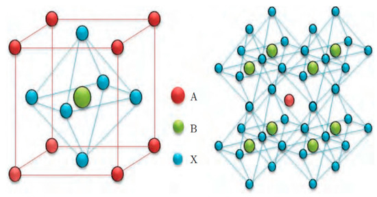
Figure 1.
Crystal structure of perovskite [8].
The most typical perovskite material, MAPbI3, has a band gap of approximately 1.55 eV, which is the optimum value of photovoltaic materials to respond to all visible light. The extinction coefficient at 550 nm can reach 1.5 × 104 cm−1 [2], and a 400 nm-thick film of this material can absorb almost all photons in the spectral range of visible light [9]. The outstanding electrical properties guarantee superior bipolar carrier transport performance of MAPbI3, which enables the diffusion length of the electron and hole to exceed 1 µm [10], and allows the carrier mobility to reach 800 cm2/V·s [11]. Moreover, the exciton-binding energy of MAPbI3 film is less than 10 meV [12], while the carrier lifetime is longer than other thin-film solar cells. In terms of device fabrication, PSCs have simple architectures with low-cost solution processing methods, making them competitive with other kinds of solar cells. In addition, PSCs can be easily prepared on flexible substrates, providing wide applications for PSCs in the future.
2.2. Device Structure of PSCs
Typical PSCs consist of a perovskite active layer sandwiched between a hole transport layer (HTL) and an electron transport layer (ETL), as well as two corresponding electrodes to collect holes and electrons. The active layer absorbs sunlight to generate electron–hole pairs, which are conducted to the fluorine doped tin oxide (FTO) and the metal electrode through the ETL and the HTL, respectively, to form a photogenerated current.
There are two common configurations of PSCs, namely, mesoporous and planar heterojunction structures, as shown in Figure 2a,b. The mesoporous PSCs are generally composed of FTO/compact ETL/mesoporous layer/perovskite/HTL/metal electrode, whereas the planar heterojunction PSCs do not have a mesoporous layer, thus, the active layer contacts directly with the compact layer. Similar to DSCs, perovskite materials in mesoporous PSCs, like dyes, infiltrate in the pores of mesoporous layers. Lee et al. replaced the TiO2 mesoporous layer with insulating Al2O3 to construct meso-superstructured PSCs. Furthermore, there are some other PSC structures, such as a C-electrode-based monolithic structure without an HTL (Figure 2c).
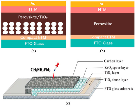
Figure 2.
(a) Mesoporous perovskite solar cell (PSC); (b) Planar heterojunction PSC; (c) Monolithic hole-conductor-free PSC [13].
3. Methodologies for Efficient PSCs
The efficiency of PSCs has been raised by a variety of approaches, such as utilizing different types of ETL and HTL, employing novel device architecture and optimizing the preparation processes. In view of the perovskite active layer, several methods can be applied to fabricate highly efficient PSCs. The chemical composition of perovskite comes first on the list of elements affecting the performance of PSCs, and different combination of ions in each site could create a continuously adjustable band gap and various crystalline phases at different temperatures, which would have a specific photovoltaic effect. The quality of perovskite film can remarkably influence the transporting properties of electrons and holes; on the one hand, the coverage and homogeneity need to be taken into consideration while, on the other hand, the grain boundaries usually exist in the perovskite film and act as recombination center that needs to be passivated. The interface between the perovskite and carrier transport layer is also of great importance in improving the PCE of PSCs. In this section, we will focus on the perovskite active layer and ascribe the increasing PCE to three aspects, described above, and review recent progress to facilitate a better understanding for researchers in PSCs.
3.1. Optimization for Chemical Composition of Perovskite
A suitable band gap is significant for the optoelectronic properties of photovoltaic materials. Absorption spectra can be adjusted through changing the band gap of perovskite materials, and a narrow band gap means more incident light can be absorbed by perovskite, while a wide one signifies higher VOC. Generally speaking, high-performance photovoltaic materials have a strong absorption band in the visible and near-infrared regions. The perovskite structures have a combination of different components which can be regulated to obtain different band gaps ranging from 1.15 eV to 3.06 eV through compositional control, to strike a balance between absorption spectra and VOC [14,15,16,17,18].
The most commonly used monovalent cation at A site is MA+, and MAPbI3 with the band gap of 1.55 eV is also ideal for single junction solar cells [19]. The ionic radius of MA+ is favorable for stable perovskite crystal structure according to the tolerance factor described by Equation (1), but FA+ is thermally more stable than MA+. Due to the narrower band gap of FAPbI3, it has a better response to near-infrared light, compared to MAPbI3. This is because the BX6 octahedra creates lattice expansion, that lowers the value of the band gap. However, organic monovalent cations are not favored by commercialization, therefore, many studies have focused on inorganic cations. On account of the constraint of tolerance factor, Cs+, with the largest ionic radius, is often employed as a monovalent cation of perovskite. In addition, Cs+ is a stable and non-radioactive monovalent cation, making CsPbI3 one of the few options for inorganic perovskites with an attractive band gap of approximately 1.7 eV that is suitable for tandems with silicon (but suboptimal for single junctions). Nevertheless, black phase CsPbI3 only occurs at higher temperatures, whereas yellow phase CsPbI3 occurs at room temperatures, and PSCs based on yellow phase only have a PCE of 0.09% [20]. The diagrammatic structure of CsPbI3 is shown in Figure 3a, and the absorbance spectra of black and yellow phases of CsPbI3 are shown in Figure 3b. It can be clearly seen that the CsPbI3 has no light absorption in most of the visible light region, leading its photovoltaic effect being extremely low. Consequently, perovskite with mixed cations has attracted researchers’ attention, in order to enhance properties of different aspects of perovskite materials [21]. For example, perovskite can be high-efficiency and thermally stable, and remains as black phase at room temperatures by applying double cation materials (MA+, FA+ or Cs+, FA+) [22,23,24,25]. Seok et al. employed double cation perovskite (FAPbI3)0.95(MAPbBr3)0.05 as active layer, which showed an efficiency of 23.2%, and stabilized efficiency of 22.85%. Remarkably, they prepared a large-scaled PSC (~1 cm2) with a PCE of 21.7% [26]. The resultant device showed better thermal stability, maintaining almost 95% of its initial performance for more than 500 h after thermal annealing at 60 °C.
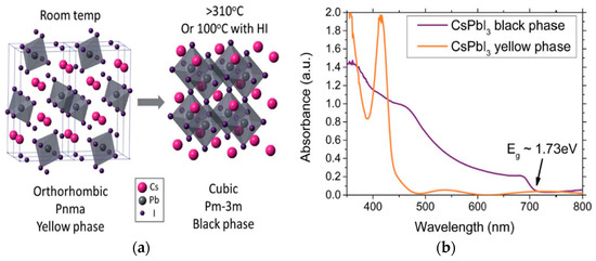
Figure 3.
(a) Crystal structure of CsPbI3; (b) Absorbance spectra of CsPbI3 [27].
In view of the excellent optoelectronic properties of double cation perovskite materials, researchers concentrated on triple cation perovskite (Cs+, MA+, FA+). Triple cation perovskite materials perform better in crystal phase stability, film quality, and environmental sensitivity, which improve the reproducibility of PSCs. Saliba et al. prepared a PSC using Csx(MA0.17FA0.83)1−xPb(Br0.17I0.83)3 as active layer, producing high-efficiency PSCs with stabilized PCE at 21.1% and output at 18%, under operational conditions, after 250 h [28]. Peng et al. obtained a high steady-state efficiency of 17.9% for MAPb3-based cells, and 19.3% for Cs0.05(MA0.17FA0.83)0.95Pb(I0.83Br0.17)3 cells, by optimizing ETL. Moreover, they demonstrated a high steady-state PCE of 16.6% for a semi-transparent cell, and used it to achieve a steady-state efficiency of 24.5% for a four-terminal perovskite–silicon tandem cell [29]. The radius of the A ion is limited by the tolerance factor, and inorganic Rb+ with a small radius is difficult to maintain in stable black phase perovskite materials. However, in the case of a multiple cation materials, Rb+ can also be applied to high-efficiency PSCs [30]. Saliba et al. found that Rb0.05FA0.95PbI3-based PSCs exhibit a best PCE of 17.16%, which is much higher than that of the FAPbI3 device, and this double cation PSC shows superior stability against high humidity (85%), under ambient conditions without encapsulation, retaining the high performance for 1000 h [31]. A summary of the research cited above is shown in Table 1.

Table 1.
Summary of researches about improving the power conversion efficiency (PCE) of PSC by optimizing chemical composition.
Pb2+ is a general component employed in B site, unfortunately, the toxicity issue of Pb2+ remains a major obstacle in the commercialization process. With the similar properties and the same main group, Sn is an ideal substitute for Pb, but Sn2+ is easily oxidized to Sn4+, which is harmful to stable perovskite crystal structure. As a result, high-performance PSCs usually utilize both Sn2+ and Pb2+ to form low-toxic perovskite materials, so as to reduce the band gap and respond to the near-infrared light [32]. Moreover, the carrier density and conductivity of the perovskite materials can be increased with a certain amount of Sn2+.
As for halide, a different anion radius of halide result in different lattice constants of the perovskite [28], and the lattice constants become larger, along with the ionic radius, and the red shift of absorption spectrum occurs [33]. It is noteworthy that the band gap of perovskite can be regulated by adjusting the I–Br ratio.
3.2. Forming High-Quality Perovskite Films by Passivating Grain Boundaries (GBs)
PSCs have frequently employed polycrystalline film as a light absorber, which creates GBs formed in the interfaces between two grains. GB tends to affect the electrical and thermal property of the material. The polycrystalline nature generates a number of GBs, as compared to their single-crystalline counterparts. In photovoltaic devices, polycrystalline materials show poor performance compared to their single-crystalline counterparts because of GBs, which are usually effective recombination centers for photon-generated electrons and holes, as well as scattering centers of free carriers. For example, silicon and CdTe-based solar cells always suffer poor performance from adverse impact induced by GBs [34,35], whereas CIS (CuInSe2) exhibited PCE as high as 20% without special GB passivation, significantly surpassing the single-crystalline CIS-based device [36]. Therefore, the influence of GBs on photovoltaic devices is still being studied in depth. When it comes to PSCs, it has been reported that GBs in CsPbX3 do not create mid-gap states, but induce very shallow states near the valence band maxima, hampering hole diffusion. For MAPbX3, similarly to CIS, GBs were found to have benign effect on optoelectronic properties [37]. However, GBs in MAPbX3 showed fast nonradiative recombination, which implies that GBs might need to be passivated.
One-step and two-step processes are commonly applied to fabricate perovskite film. Citing MAPbI3 as example, a one-step method is performed by spin-coating a solution of CH3NH3I (MAI) and PbI2 in organic solvents to form the photoactive layer of MAPbI3, while the so-called two-step process is performed by spin-coating a mixed solution of MAI and PbI2 onto the substrate. The perovskite film prepared by the two-step process has a higher film quality, better coverage on the substrate and, also, higher permeability in the mesoporous layer for mesoporous PSCs [38]. When considering time for the production of PSCs in industry, one-step is expected to be a more desirable process because it will reduce the time for perovskite coating and, thereby, fabrication of PCSs. Thus, retarding crystallization or controlling crystal growth is important step in a one-step procedure.
Roldan-Carmona et al. found that an excess of PbI2 improves the average fill factor (FF) and VOC, boosting the average PCE from 16.2% to values close to 18% [39]. It can be seen, from the results of scanning electron microscopy (SEM) and time resolved photoluminescence (TRPL), that an excess of PbI2 also improves the crystallinity of the film and the lifetime of the carriers. The same phenomenon can be discovered in perovskite with mixed cations [40]. Kim et al. also reported that the performance was greatly improved by incorporating some amount of PbI2 into MAPbI3. In addition, positive effects of PbI2 incorporation were also extended to (FAPbI3)0.85(MAPbBr3)0.15, yielding similar performance improvements as the MAPbI3 cells. Nevertheless, it will have a negative impact on the quality of the perovskite film if the amount of PbI2 is not precisely controlled [41,42].
Park and co-workers studied the effects of excess MAI on the properties of perovskite materials [43]. The non-stoichiometric precursor solutions are prepared by mixing MAI, PbI2, and DMSO in DMF, where the molar ratio of PbI2/MAI is changed from 1:1 to 1:1.02, 1:1.04, 1:1.06, 1:1.08, and 1:1.1 (x = 0, 0.02, 0.04, 0.06, 0.08, and 0.1). The coating process is presented schematically in Figure 4a. After the spin-coating process, intermediate (MAI)1+xPbI2DMSO can be formed, which provides an effective method to obtain high-quality perovskite films and achieve highly efficient device performance [44,45]. The short circuit photocurrent density (JSC) hardly changes up to x = 0.06, but declines slightly for x = 0.08 and 0.1. On the other hand, both the VOC and FF are increased as x is enhanced to 0.06. As a result, the average PCE reaches a maximum of 19.8% for x = 0.06. The results of transmission electron microscopy (TEM) showed that the stepped edges of grains disappear in the presence of excess MAI, which is indicative of a modification of the surface of perovskite grains by excess MAI. It can be seen from the results of conductive atomic force microscopy (c-AFM) (Figure 4b,c) that GBs show a brighter contrast, which indicates that the GB carries the current more efficiently.
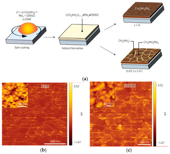
Figure 4.
(a) Schematic illustration of the one-step coating process with and without MAI; c-AFM images of MAPbI3 films with excess MAI for (b) x = 0; (c) x = 0.06 [43].
Apart from the methods of non-stoichiometric precursors, utilizing of some additives can also serve as an effective approach to achieve interface passivation, so that the performance and stability of PSCs can be improved. In 2018, Zheng et al. employed hexamethylenetetramine (HMTA) as an additive to passivate MAPbI3 film and, thereby, advance cell optoelectronic performance [46]. The perovskite surface, fully covered by HMTA, is modified by forming a stable insulation layer to bridge across the GBs. Additionally, HMTA can coordinate Pb2+ on the perovskite surface, facilitating the disappearance of PbI2 and formation of pure perovskite nanocrystals [47], which can be seen in Figure 5a. HMTA can also serve as nucleation control reagent, facilitating perovskite to form an aligned orientation. Lastly, HMTA can cover the ZnO thin film to enhance the adhesion of perovskite with the oxide substrate. Owing to these beneficial advantages of HMTA, both PCE and reproducibility were highly improved. Li et al. introduced a large molecular organic dye AQ310 with −COOH functional group as passivator to reduce the trap states of the perovskites and promote better stability [48]. Carboxyl has been effectively used in other photovoltaic devices as an indispensable anchoring group, due to the strong coordination with metal oxide [49]. Similar to HMTA, the carboxyl of AQ310 coordinates with under-coordinated Pb2+, as shown in Figure 5b, thereby reducing the trap states of under-coordinated Pb2+, prolonging the carrier recombination time and, thus, leading to the enhancement of VOC. In addition, other additives, such as fullerene derivatives [6,6]-phenyl-C61-butyric acid methyl ester (PCBM) [50], PEA+ [51], nitrogen-doped carbon dots (NCDs) [52], and others, are also utilized to incorporate with perovskite precursor to achieve passivation of the GBs for improved efficiency and stability. Various GB passivators used in perovskite materials, mentioned above, are summarized in Table 2.
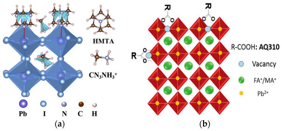
Figure 5.
Crystal structure of perovskite passivated by (a) hexamethylenetetramine (HMTA) [46] and (b) AQ310 [48].
Table 2.
Summary of research about improving the PCE of PSC by passivating grain boundaries (GBs).
3.3. Modification of Interface
The reasonable design of the device structure, in order to obtain great properties such as energy level matching, is also one of the crucial factors affecting the performance of PSCs, apart from passivating the GBs, to achieve a certain morphology and coverage of the perovskite film. PSCs are composed of perovskite layer, carrier transport layer, and electrode, in which many interfaces exist between the different layers. There are some factors that decrease the efficiency and other properties of PSCs in these interfaces, for example, the barrier hindering the transportation of electrons or holes, the recombination center caused by surface defects, and insufficient contact between perovskite layer and the carrier transport layer. Consequently, these problems can be solved through surface and interface engineering, thereby producing a better efficiency of PSCs.
PSCs have usually employed TiO2 as a mesoporous layer, owing to its wide band gap, good chemical stability, and high light transmittance [53]. Meanwhile, TiO2 with a mesoporous structure has a large specific surface area which can effectively contain perovskite materials, ensuring sufficient contact between the perovskite layer and the mesoporous layer, thereby improving the efficiency of collecting the electrons. Unfortunately, abundant oxygen vacancies, high density of electronic trap states, and low electron mobility of TiO2 might cause undesirable charge accumulation and recombination, degrading the PCE of PSCs [54].
Metal oxides are often utilized as interface modification layers in PSCs. In 2017, Wang et al. reported an efficient PSC engineering by inserting Al2O3/NiO layers in between the ETL and absorber layer [55], and the device structure is illustrated in Figure 6a. From the device structure, we can see that the presence of NiO accelerates the transporting of hole, and insulating Al2O3 limits the electrons within the perovskite layer, so that the transporting of electrons can be quite effective. Additionally, the Al2O3/NiO interfacial engineering improves the crystalline quality of perovskite films, and effectively suppresses carrier recombination. The devices showed a maximum PCE of 18.14% and remarkable long-term air-stability, retaining ~86% of PCE over 210 days under an ambient environment. Shaikh et al. employed ZnS as an interfacial modifier between mesoporous TiO2 and a MAPbI3 absorber layer, via the successive ionic layer adsorption and reaction method (SILAR) [56]. The ZnS-modified layer helps in suppressing the backflow of electrons, effectively reducing interfacial charge recombination and facilitating electron transfer. Wang et al. modify the TiO2/MAPbI3 interface by introducing 3-aminopropyltrimethoxysilane (APMS) [57]. APMS hydrolysate can enhance the wettability of perovskite precursor on the TiO2 surface, forming a perfect MAPbI3 film, and increasing the recombination resistance at the interface.
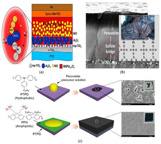
Figure 6.
(a) Schematic of device configuration of PSC with Al2O3/NiO interlayer and carrier working paths [55]; (b) Schematic illustration of alkali-TFSI salt-doped mesoporous layer, and the surface states bonding with electron transport layer (ETL) and perovskite [60]; (c) Schematic illustrations of perovskite film formation on organic hole transport layer (HTLs) with and without the interfacial compatibilizer PFN, and corresponding photographs and SEM images [62].
The interface between perovskite and HTL is also a vital issue because of energy level matching and recombination of the charge carrier. Lu et al. achieved the modification of the interface between the perovskite and HTL with commercially available para-substituted benzenethiol molecules, with both improved efficiency and stability [58]. The interlayer modulates the band alignment at the perovskite/HTL interface, which could assist charge extraction and suppress carrier recombination. These effects create a high efficiency of more than 20%. During the process of preparing a perovskite film, there will frequently be non-uniformity and pinholes, with the exception of surface defects. With the aim of overcoming this problem, Wang et al. reported the improvement of the photovoltaic performance and stability of PSCs through the insertion of a solution-processed poly(methyl methacrylate) (PMMA) layer between perovskite and HTL [59]. It can be seen that the perovskite layer, without a PMMA layer, exhibited greater roughness than that with a PMMA layer. The PCE of this PSC increased to 18.1%, and the stability decreased by only about 5% during 20 days of exposure in moisture ambient conditions.
Post treatment and some additives can also effectively control the carrier’s behavior of the perovskite layer/carrier transport layer interface. Singh et al. reported the incorporation of alkali metal dopants in mesoporous TiO2, which can effectively modulate electronic conductivity and improve the charge extraction process by counterbalancing oxygen vacancies acting as nonradiative recombination centers [60]. Sulfate bridges (SO42−), from the alkali-bis(trifluoromethanesulfonyl)imide (alkali-TFSI) salts grafted on the surface of mesoporous TiO2, provide a seamless integration of absorber and electron-transporting layers that accelerates the overall transport kinetics, resulting in a high efficiency of 21.1%; the schematic illustration can be seen in Figure 6b. Zheng et al. employed crosslinkable radical copolymer poly (2,2,6,6-tetramethylpiperidinyloxy-4-yl methacrylate)-co-(4-benzoylphenyl methacrylate) (PTMA–BP) to engineer the surface of the poly(3,4-ethylenedioxythiophene): polystyrene sulfonate (PEDOT: PSS) HTL layer [61]. They found that PTMA–BP can induce better band alignment between HTL and perovskite, reduce the interfacial charge carrier recombination, and improve crystallization of perovskite hybrids that are cast on top of the HTL. Lee et al. introduced amphiphilic conjugated polyelectrolyte poly[(9,9-bis(3′-(N,N-dimethylamino)propyl)-2,7-fluorene)-alt-2,7-(9,9-dioctylfluorene)] (PFN) as an interfacial compatibilizer, constructing uniform perovskite films on large-area substrates; a schematic illustration of perovskite film formation is shown in Figure 6c [62]. Remarkably, they obtained the best PCE of 17%, which is the highest value for printable PSCs with a total active area larger than 1 cm2. The literature on interfacial modifications, cited above, are summarized in Table 3.
Table 3.
Summary of research about improving the PCE of PSC by interfacial engineering.
4. Analysis and Recent Progress of Stable PSCs
The efficiency of PSCs has been raised from 3.8% to 23.3% in just nine years, which is quite impressive compared to other thin-film solar cells that have been developed for decades. However, the stability of PSCs still remains a troublesome problem that has not been solved well, and most high-stability PSCs have a short lifetime of just around one year [63], which is a primary obstacle for the commercialization of PSCs [23]. The injection of moisture and oxygen is the main reason for the instability of PSCs, followed by thermal and ultraviolet (UV) stress. Hybrid perovskite materials may degrade in humid conditions, and suffer phase transition and thermal decomposition under fluctuation of temperature. The irradiation of UV not only reduces the stability of the perovskite materials, but also causes photocatalysis at the interface of TiO2 when it is used as ETL. In this section, we will elaborate upon the instability of PSCs caused by ambient air, temperature, and UV irradiation, and summarize recent progress in improving the stability of PSCs. Some studies about PSC stability, cited below, are summarized in Table 4.
Table 4.
Summary of literatures about stability of PSC.
4.1. Moisture and Oxygen Stability
When the typical perovskite material MAPbI3 is exposed to ambient conditions, the reactions will occur as follows [64]:
CH3NH3PbI3 (s) → CH3NH3I (aq) + PbI2 (s),
CH3NH3I (aq) → CH3NH2 (aq) + HI (aq),
4HI (aq) + O2 (g) → 2I2 (s) + 2H2O,
2HI (aq) → H2 (g) + I2 (g).
MAPbI3 is highly sensitive to the environment, moisture and oxygen from ambient conditions, thermal stress, and even residual solvents, which can cause the decomposition of perovskite. MAPbI3 degrades in the presence H2O, as illustrated in Equation (2). The equilibrium of Equation (3) results in the coexistence of HI, CH3NH2, and CH3NH3I in the film. There are two ways for HI to degrade for the next step. One is the redox reaction, in the presence of oxygen, stated in Equation (4). Another consists of the photochemical reaction, whereby HI decomposes in the presence of UV radiation into I2 and H2, which is demonstrated in Equation (5). The consumption of HI drives the whole degradation process to move forward. We can observe, from the reactions mentioned above, that moisture and oxygen are destructive to perovskite materials and, thus, the majority of the fabrication processes must be carried out in a glove box under an inert atmosphere [65]. The performance of PSCs shows a sharp decline as the perovskite decomposes, which is a huge challenge for the application of PSCs.
Modification of the halide composition of perovskite materials was reported to be an effective way to improve the stability of the materials. The mixture of multiple halogen elements in perovskite materials brings many positive effects, including an improvement in carrier transport and regulation of band gap. Lee et al. reported that the stability of air-processed MAPbI3−xClx was significantly improved compared with air-processed MAPbI3 [4]. Jeon demonstrated that the incorporation of Br into MAPbI3 can effectively enhance its stability performance [66]. Zhu et al. employed a facile halide exchange route to incorporate Br into MAPbI3 to form MAPbI3−xBrx, yielding a maximum PCE of 14.25%, and 93% of the original efficiency was retained after exposure to ambient air for 14 days without encapsulation [67].
The stability of the perovskite film has been improved with incorporating mixed halides, but halide segregation still remains a problem for the long-term stability of the PSCs [68]. As a result, cation substitution in PSCs was proposed as a further enhancement for improved device stability. It has been mentioned above that mixed cations result in a great improvement in optoelectronic properties. Actually, the incorporation of FA+ and Cs+ has some benefits for stability. FAPbI3 has a larger tolerance factor and a more stable crystal structure than conventional MAPbI3, such that many reports have introduced perovskite of FA+ and MA+ hybrid cations to lift the stability of devices [69,70]. Mixed-cation materials, such as Cs/MA, Cs/FA, and Cs/MA/FA, could also improve the stability as affected by humidity and oxygen [20,22,28]. Additionally, perovskite materials based on Cs+ with triple halide also have a remarkable stability against moisture and oxygen stress [71,72].
In order to lessen the effect of ambient air on the stability of the PSCs, some studies have introduced a waterproof tunnel layer in the PSCs. Wang et al. employed polystyrene (PS), Teflon, and polyvinylidene–trifluoroethylene copolymer (PVDF–TrFE) as tunneling materials [73]. They demonstrated that the tunneling layer can serve as an encapsulation layer to prevent perovskite film from damage caused by water. Inserting a tunneling layer between perovskite and ETL could also significantly increase device performance by suppressing carrier recombination at the point of cathode contact. Additionally, Zr acetylacetonates (ZrAcac) [74], benzylamine (BA) [75], and (N4,N4′-Di(naphthalen-1-yl)-N4,N4′-bis(4-vinylphenyl)biphenyl-4,4′-diamine) (VNPB) [76] were recently utilized as an isolated layer, to improve the stability of PSCs against ambient air.
4.2. Thermal Stability
Thermal stability also raises a lot of concerns, due to the impact on performance of PSCs. Operating temperatures of deployed solar cells can vary from −40 °C to 85 °C and, depending on their location, solar cells must have the ability to work under high-temperature conditions, in particular. Conings et al. employed X-ray diffraction (XRD), X-ray photoelectron spectroscopy (XPS), PL, and AFM measurements to convincingly demonstrate that MAPbI3 does degrade at 85 °C, even in inert conditions, indicating the poor stability under thermal stress [69]. MAPbI3 has a low thermal conductivity [77], and the heat caused by light irradiation cannot be removed easily, thus making thermal stability worse for PSCs. The decomposition resulting from high temperature is simply due to evolution of the organic components, such as HI and CH3NH2, leaving behind PbI2. This process is more intense when the PSCs are exposed to ambient air. Therefore, MAPbI3 cannot be considered as a promising compound for long term operation at elevated temperatures. Snaith and co-workers successfully made PSCs using CsPbI2Br, which exhibited greatly enhanced thermal stability, not decomposing even at 180 °C over 30 min (Figure 7a,b), a temperature at which MAPbI3 decomposed within 5 min [78]. However, the crystal structure of inorganic perovskite materials is highly sensitive to variations of temperature, and the performance is not eligible because inorganic perovskite materials cannot form a stable black phase with good optoelectronic properties at room temperature. Replacing MA+ with the larger and heavier FA+ is another option for raising the thermal stability of PSCs. Eperon et al. compared films of MAPbI3 and FAPbI3 heated at 150 °C in air, to show that the FAPbI3 did not degrade over 60 min, while the MAPbI3 had almost completely converted to PbI2 (Figure 7c) [79]. In addition, mixed cations with FA+ and Cs+ also showed an outstanding thermal stability [80].
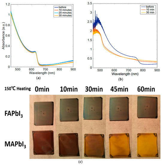
Figure 7.
Absorption spectra for CsPbI2Br (a) and MAPbI3 (b) after heating at 180 °C [78]; (c) Thermal degradation of MAPbI3 and FAPbI3, when bare spin-coated films of each perovskite are heated in air at 150 °C for the times indicated [79].
The fluctuation of temperature also affects crystal structure of perovskite and, thereby, performance of PSCs. Conventional MAPbI3 exists in a perovskite phase with tetragonal distortion at room temperature. The symmetry is further reduced at lower temperatures, as the material enters an orthorhombic phase, while it is increased with higher temperatures about 60 °C as it transitions to the cubic phase [81]. Considering the operating temperature of the solar cells, the crystal structure of MAPbI3 is basically maintained on the tetragonal and cubic phase, and the lattice distortion has little harmful effect on PSCs based on MAPbI3. Due to the decomposition of MAPbI3 up to 85 °C, researchers pay more attention to crystal structure stability of FAPbI3 and CsPbI3, which are not easily decomposed at high temperatures. The larger size of the FA+, however, means that FAPbI3 does not form a black, cubic, or tetragonal perovskite phase at room temperature, but exists as a yellow film consisting of a hexagonal non-perovskite phase. Annealing at temperatures above the tetragonal phase transition (150 °C) allows a black perovskite phase to be formed, which is retained after cooling to room temperature [79]. In order to lower the tolerance factor and prevent the appearance of a hexagonal phase, double cation perovskite with MA+ and FA+ can be employed, leading to an effective tolerance factor close to 1, allowing a black cubic perovskite phase to be easily formed at low temperatures, and to be stable at room temperature. Inorganic CsPbI3 does not form a stable perovskite phase at room temperature, but exists in a yellow orthorhombic phase which has an extremely low photovoltaic effect. The crystal structure of CsPbI3 is very sensitive to temperature, and needs to be annealed at a high temperature, up to 300 °C, to form a cubic phase. CsPbBr3 can be prepared and is structurally stable at room temperature, but has an unsuitably high band gap over 2.3 eV. Mixing both I and Br, and reducing the size of the metal halide octahedral, is an approach to stabilize CsPbX3 structures with appropriate band gaps. Beal et al. made a fully inorganic perovskite with incorporation of Br above 20%, that exists in the cubic phase at room temperature after annealing, exhibits excellent thermal stability, and has band gaps (1.7–1.9 eV) suitable for perovskite–silicon or perovskite–perovskite tandems [78]. Swarnkar et al. fabricated phase-stable CsPbI3 quantum dots, highlighting the link between structural and atmospheric stability [82].
Th widely used HTL material, spiro-OMeTAD, is another reason for poor thermal stability of PSCs. Spiro-OMeTAD is prone to crystallization, which affects the contact between the absorber and the HTL inside the pores, or on the interface, as the temperature elevates [83]. On the other hand, spiro-OMeTAD requires two other additives, namely, bis(trifluoromethane) sulfonamide lithium salt (Li-TFSI) and 4-tert-butylpyridine (TBP), to process. TBP will cause degradation of the perovskite layer due to the corrosive effect [84]. For the purpose of solving the thermal stability problem caused by spiro-OMeTAD, inorganic hole-transporting material [85], or other kind of additives, could be used [86].
Low dimensional perovskite materials have been the subject of wide attention in recent years, owing to their stable crystal structure, high formation energy [87], low self-doping concentrations [88], and suppressed ion migration [89]. The low dimensional perovskite structure can be visualized to cut the three dimensional (3D) perovskite structure along the <100> orientation, building BX42− octahedral layers, followed by inserting bulkier organic molecules that replace the position of small molecules such as MA+, forming two dimensional (2D) perovskite with a sheet structure, due to the increase in the distance between the layers (Figure 8) [90]. Bulkier organic molecules and inorganic layers are combined with van Der Waals forces. This self-assembly process results in a significant increase in the formation energy, thereby enhancing the stability of perovskite. Furthermore, hydrophobic bulkier organic molecules form a natural encapsulation layer, excluding water or oxygen from the atmosphere. Therefore, low dimensional perovskite is of great significance for stable PSCs.
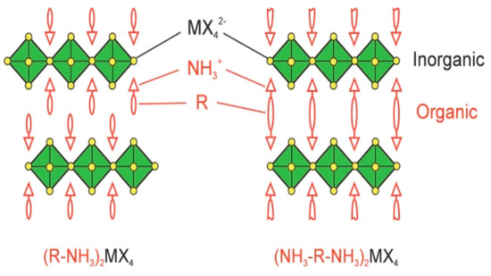
Figure 8.
Schematic representation of low dimensional perovskite [90].
The number of layers of low dimensional perovskite varies by adjusting the ratio of the reactants in the precursor, and low dimensional perovskite can be easily prepared through simple one-step spin-coating. However, these layers have a large band gap [91], and bulkier organic molecules could reduce the mobility of electrons and holes [92]. These problems restrict the performance of PSCs with low dimensional materials, such that the original low dimensional PSC only achieved an efficiency of 4.37% [93]. Finding an optimum number of inorganic layers, choosing appropriate organic amine molecules, and exploring the vertical growth of low dimensional perovskite crystals can create PSCs with a stable crystal structure and high efficiency.
4.3. UV Stability
In the PSCs, TiO2 is frequently used as electron transport material, due to its good chemical stability, resistance to corrosion, non-toxicity, and low cost. Unfortunately, because of the redox property and band gap of 3.2 eV, TiO2 can also serve as a photocatalytic material, oxidizing water or some organic materials to produce OH radical [94]. Leijtens et al. demonstrated that the TiO2 layer in PSCs is susceptible to UV-induced degradation [95]. Ito et al. found that, after exposure to light, MAPbI3 transformed to PbI2, due to the contact between perovskite and TiO2 [96]. The degradation in the film, caused by exposure to UV light, has been explained as follows [64]:
2I− → I2 + 2e−,
3CH3NH3+ → 3CH3NH2 + 3H+,
I− + I2 + 3H+ + 2e− → 3HI.
TiO2 extracts the electron from I−, and then breaks the perovskite structure, creating the production of I2, as explained by Equation (6). CH3NH3+ decomposes and releases gases of CH3NH2 and H+ (Equation (7)). I− react with I2 and H+, producing HI. The incessant elimination of HI and evaporation of CH3NH2 move Equation (6) and (7) forward, finally leading to decomposition of perovskite.
In order to overcome difficulty inducing by UV light, Snaith and co-workers replaced mesoporous TiO2 with insulating mesoporous Al2O3 scaffold, showing a better stability of 1000 h with AM 1.5 illumination at 40 °C with no UV cutoff filter [95]. However, there is some initial deterioration in the FF and VOC of the cells over the first 200 h of exposure. Roose et al. employed Ga-doped mesoporous SnO2 as a scaffold layer [97]. Gallium severely decreases the trap state density in SnO2, leading to a lower recombination rate and a stabilized PCE of 16.4%. PSCs based on mesoporous TiO2 absorbed more UV light compared to Ga–SnO2, which can be seen in the UV/visible absorption spectra, implying a better UV stability. Some novel electron transport materials can be utilized as substitution of TiO2. Yin et al. applied 2D-TiS2 as an effective electron transport layer in planar PSCs [98]. TiS2 has similar properties to TiO2, including the ability of electron transportation and band alignment, ensuring high efficiency of devices. The results of Figure 9 manifest that PSCs with TiO2 showed a strong photocatalysis, whereas PSCs with TiS2 did not show the same phenomenon. The efficiencies of PSCs with TiS2 were decayed by only about 10% from its maximum value after continuous illumination under UV light for 50 h. Unlike the replacement of the TiO2 ETL, Tsai et al. introduced biaxially-extended octithiophene-based conjugated polymers which could filter UV light in inverted PSCs, in other words, the irradiation of UV light could be blocked by HTL [99]. There are some other reports that used down-conversion materials and a UV-blocking layer in PSCs to improve stability in UV light [100,101].
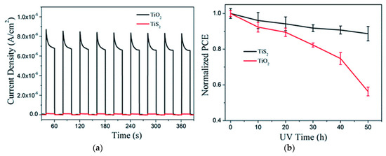
Figure 9.
(a) Ultraviolet photocatalytic activity for decomposition of water in Na2SO4 solution by using TiO2 and on TiS2 film on FTO glass as photoanodes; (b) Long-term UV light stability of the PSCs with TiO2 or TiS2 film as the ETLs [98].
5. Routes toward Low-Cost PSCs
The trade-off between cost and efficiency is still a major obstacle for commercialization of PSCs. Although silicon solar cells that are commercialized already have an abundance of silica as raw materials, complicated manufacturing process, and efficiencies ranging between 21% and 25%, are the major drawbacks. Evolved PSCs can be prepared through a simple and low-cost solution process, making PSCs a promising substitute of silicon solar cells. The organic solid hole-transporting materials, such as spiro-OMeTAD [3], poly[bis(4-phenyl)(2,4,6-trimethylphenyl)amine] (PTAA) [102], and poly(3-hexylthiophene-2,5-diyl) (P3HT) [103], were employed because of degradation caused by liquid electrolyte, however, bring the problem of high cost to the fabrication of PSCs. It has been reported that organic HTL precursor and processing alone covers 33.9% of the device cost, due to the complicated synthesis processes (Figure 10) [104]. In the pursuit of low-cost PSCs, the inorganic hole transport materials (HTM), like CuI [105], CuSCN [106], and NiO [107,108,109,110,], have been applied to replace expensive organic materials.
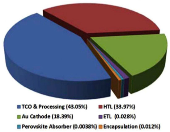
Figure 10.
Price sharing of precursors of each layer of a conventional PSC [104].
5.1. Replacement of Costly Organic Hole-Transporting Materials and Hole-Conductor-Free PSCs
Materials of HTL can be divided into inorganic, organic, and hybrid materials, while organic materials can be further subdivided into small molecule and polymer [111]. Following on from the experience of solid state dye-sensitized solar cells, of the organic materials currently used to make the best devices, spiro-OMeTAD has long been the benchmark HTM against which other materials have been compared. However, its cost is about 5 or 6 times higher than the gold, so low-cost HTM is in great demand. The development in inorganic HTMs has been rather slow compared to organic HTMs, and only a limited number of inorganic materials have been tested. Copper salts, like CuI, Cu2O, and CuSCN, and NiO, which is most widely-studied inorganic HTM, are relatively inexpensive and stable under ambient conditions; the copper salts do not require doping to achieve good hole mobilities, and the devices show good stability. Nevertheless, PSCs using inorganic HTMs cannot gain a sufficient PCE compared with PSCs based on organic HTMs, and the solvents used for inorganic HTMs can partially dissolve the active layer, thus causing device instability. Moreover, some materials, while inexpensive, must be deposited by more expensive methods, such as sputtering, and the extra fabrication costs are likely to cancel out any advantages in price of materials.
Perovskite materials offer an electrically conductive path for both p-type and n-type charge carriers [112,113,114], and electrons and holes both have a long diffusion length inside the perovskite [115,116], which means the perovskite layer can transport holes effectively, even if without HTL. From the view of band alignment, as long as electrode material satisfies matching the conditions of energy level and work function, that is, the HOMO is higher than the valence band of the perovskite (~5.3 eV), the holes can be effectively transported, and the band alignment of hole-conductor-free device-based Au electrode is shown in Figure 11a. Therefore, it is theoretically feasible to remove the HTL directly.
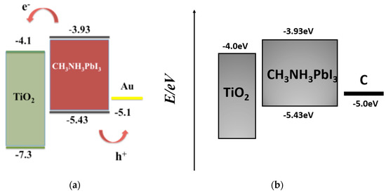
Figure 11.
Band alignment of hole-conductor-free device-based (a) Au electrode [117] and (b) C electrode.
In 2012, Grätzel and co-workers reported PSC without HTL for the first time, and exhibited a promising PCE of 5.5% [117]. The synthesis of MAPbI3 and deposition on the mesoporous TiO2 film was carried out by spin-coating, and then Au was deposited directly onto the perovskite layer by thermal evaporation. Etgar et al. prepared hole-conductor-free PSCs, and further enhanced the efficiency to 10.85% [118]. Ma et al. fabricated a hole-conductor-free PSC based on CsPbIBr2, achieving a PCE of 4.7% and excellent thermal stability [119].
Metal–semiconductor contact is formed in PSCs due to the removal of HTL, which is detrimental to the separation of electrons and holes in the interface. The direct contact between the perovskite layer and Au electrode leads to an energy barrier of about 0.24 eV, as well as a depleted region over 60 nm existing in the back contact region [120], causing a reversed effect in transportation of carriers and low internal quantum efficiency (IQE) in the long-wavelength region. Furthermore, interface recombination, caused by defects, also affects the performance of hole-conductor-free PSCs. Homogeneous perovskite film and thicker mesoporous layers are always required so as to form better metal–semiconductor contact and avoid short circuits. Shi et al. increased the concentration of PbI2 in spin-coating precursors, reduced the spin-coating speed, and then prepared a uniform film with appropriate thickness. The metal electrode was directly evaporated onto perovskite, achieving a PCE of 10.47% [120].
The introduction of isolated layers can overcome recombination in the interface between electrode and perovskite. Wei et al. introduced ultrathin insulator AlOx film into the MAPbI3/Au interface by atomic layer deposition (ALD) technology, and the ALD deposition cycles were further optimized [121]. The average PCE of the cell has been enhanced from 8.61% to 10.07%, with the highest PCE of 11.10%. The presence of AlOx significantly enhanced the IQE of the cell in the long wavelength region, leading to the increase in photocurrent. Xu et al. employed N,N,N′,N′-tetraphenyl-benzidine (TPB) by spin-coating to engineer the metal–semiconductor interface in the hole-conductor-free PSCs [122], and the thin TPB layer increased recombination resistance, resulting in a lower recombination rate in the interface.
5.2. Carbon Electrode for PSCs
Another bottleneck in PSC is the high cost and complexity involved in the Au or Ag back electrode deposition. Noble metal and processing covers 18.3% of the device cost (Figure 10) [104]. The appropriate 5.0 eV work function, near to that of Au (5.1 eV), makes carbon an ideal candidate for PSCs’ back electrode, so, similar to the PSCs base on noble metal, hole-conductor-free PSCs using carbon as electrode can transport holes effectively without HTL (Figure 11b). Being abundantly available on the earth, carbon is also known for good conductivity, electrochemical activity, water resistance, high chemical stability, and flexibility in processing, leading to low-cost and high-efficiency PSCs [123]. Undoubtedly, carbon is an attractive choice for back electrode in hole-conductor-free PSCs.
To the best of our knowledge, the highest efficiency achieved by hole-conductor-free PSCs utilizing carbon as back electrode is 15.9% [124]. According to the different bonded patterns of carbon atoms and different dimensions of crystalline structures, there are several allotropes with very different chemical and physical properties, as shown in Figure 12. Carbon nanotubes (CNTs) have a particular 1D hollow tubular structure, which can be considered as the result of rolling up a monolayer graphite sheet, resulting in a strong ability charge absorption [125]. The CNTs have good conductivity and chemical stability, and the electrical properties can be adjusted by chemical doping [126]. Nanoscale CNTs can also be applied to flexible PSCs, building wearable photovoltaic devices, meanwhile, CNTs have a good transmittance of sunlight, causing more incident light for PSCs. Single-walled carbon nanotubes (SWCNTs) and multi-walled carbon nanotubes (MWCNTs) are the most common species of CNTs. Graphite is a soft and hexagonal laminated material, which has an outstanding thermal and electrical conductivity and high corrosion resistance, however, it is often mixed with amorphous carbon black with a large specific surface to form carbon paste, in order to contact effectively with perovskite layer. Graphene could be employed in all layers of PSCs, which is called a “universal material”. Apparently, graphene is a promising candidate for noble metals, owing to the good chemical and thermal stability and high carrier mobility.
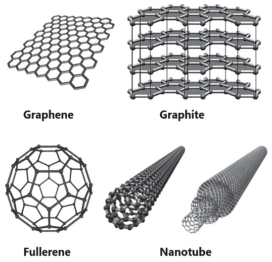
Figure 12.
Structure of various carbon materials [127].
Li et al. introduced CNTs in PSCs as back electrode, for the first time, in 2014 [126]. They applied the floating catalyst chemical vapor deposition method to fabricate laminated CNT networks, and then introduced it in hole-conductor-free PSCs, obtaining a PCE of 6.87%. By adding spiro-OMeTAD to form a composite electrode, the efficiency of this device can be further improved to 9.9%, due to the better enhanced hole-extraction and reduced charge recombination. Inspired by this work, plenty of studies mixed CNTs with hole transport materials [128,129,130,131], whereafter, some researchers utilized CNT alone as back electrode, by optimizing the device structure and preparation process [132,133,134].
In 2013, Han et al. established a hole-conductor-free MAPbI3/TiO2 heterojunction solar cell, which first introduced carbon black/spheroidal graphite as a back electrode to substitute the noble metallic electrode [13]. Mesoporous TiO2 and isolated ZrO2 with a thickness of 1 µm was screen-printed on the top of the TiO2 compact layer, then, the 10 µm carbon back electrode was deposited followed by dipping of MAPbI3 precursor on top of the mesoscopic carbon layer, creating a structure of FTO/TiO2 compact layer/TiO2 mesoporous layer/ZrO2 isolating layer/carbon back electrode. This kind of structure is a so-called monolithic structure, as shown in Figure 2c, with an impressive PCE, exceeding 6.64%, and the device showed a long-term stability in the dark after 840 h. The sufficient infiltration of the perovskite precursor [135], quality of the perovskite materials [136], the size of TiO2 particles [137], and the thickness of ZrO2 [138], all affect the performance of monolithic PSCs.
The mass ratio of the composite materials of graphite and carbon black significantly influences the contact between the back electrode and the perovskite layer and electrical conductivity of the electrode itself. Graphite has good electrical conductivity, and plays a major role in the process of carrier conduction, but excess content of graphite will cause insufficient internal contact, thereby increasing electrical resistivity. Therefore, a moderate amount of carbon black is employed to obtain a better contact between graphite flakes [139]. The perovskite materials are filled in the porous carbon electrode of monolithic PSCs mentioned above, and an appropriate pore size can also determine the performance of monolithic PSCs. Zhang et al. found that 8 µm graphite is suitable for PSC electrodes and the optimum electrodes have a smaller square resistance and, hence, help the PCE exceed 11% [140].
Graphite, carbon black, and binder additives can be mixed to fabricate the commercial conductive carbon pastes which are widely used in PSCs. Tao et al. reported a carbon back electrode assisted by polystyrene spheres (PS-spheres) as pore-forming agent to gain microporous structure, for a better permeability with an average efficiency enhancement of 22% [141]. Liu et al. applied low-temperature carbon back electrode in fabricating large-area hole-conductor-free PSCs, achieving a PCE of 3.3%, and with no obvious decay during a testing period of 624 h [142]. Zhang et al. fabricated a monolithic PSC using carbon as back electrodes and TiO2 nanosheet layers as photoanode. With the increasing thickness of TiO2 nanosheet layer, more MAPbI3 was adsorbed into the TiO2 nanosheet photoanode, and the interfacial recombination of electrons and holes at TiO2 nanosheet/perovskite interface was reduced, leading to the higher JSC and VOC [143]. Hari Bala and co-workers optimized the doping ratio of Br in perovskite, making the device retain 96.23% of the initial efficiency after being stored in the air for 56 days (1344 h) [144]. Li et al. prepared Ag/nano-TiO2 composites and introduced them into the compact film of conventional hole-conductor-free PSCs. The strong scattering effect and the surface plasmon resonance effect of the metallic Ag nanoparticles strengthened the optical absorption of the PSCs in the visible light region, and enhanced the efficiency of electron injection, resulting in a 30% enhancement in PCE [145].
In 2004, Novoselov et al. prepared graphene by mechanical exfoliation (repeated peeling) of small mesas of graphite [146]. At present, graphene is widely used in the fields of chemistry and materials science, and plays a more and more vital part in the photovoltaic field. Snaith and co-workers employed graphene to PSCs, firstly, and utilized nanocomposites of graphene and TiO2 nanoparticles as the electron collection layers in mesoporous PSCs, providing superior charge-collection ability [147]. Not only being used in the ETL, graphene can be a functional material of transparent electrodes [148,149,150] and HTL [151,152,153]. In terms of the back electrodes, Yan et al. synthesized single-layered graphene (SG) and multi-layered graphene (MG) from the reduction of their oxide at 1000 °C under an argon atmosphere, and then utilized these graphene materials as back electrodes [154]. After detailed investigation, they found that MG has higher hole extraction rates than SG. PSCs used MG as HTL yield about 11.5% PCE, with FF as high as 0.73, whereas SG devices yield 6.7% and 0.54. Wei et al. synthesized three-dimensional honeycomb-like structured graphene (3DHG) by the reaction of potassium with CO2, which is coated on a perovskite layer as a back electrode with the doctor-blade method [155]. The electrical conductivity of 3DHG can be enhanced through increasing synthesis time, thereby boosting the performance, and hysteresis was not observed for the PSCs with the 3DHG back electrode. Zhu et al. synthesized high specific surface area nitrogen-doped graphene frameworks by using a facile one-step fast pyrolysis [156]. The PCE of 10.32% is achieved, higher than devices with a purely graphene framework as back electrode. The enhancement can be attributed to the increased charge-extraction efficiency and transportation ability, which reduce charge-recombination losses. Additionally, the large light transmittance of graphene makes it an excellent electrode material for top cells of tandem photovoltaics [157,158,159].
5.3. Scalable Deposition Methods
High-performance PSCs are fabricated through solution processing, which has not been demonstrated for other photovoltaic technologies. This makes PSCs promising candidates for a high-performance, low-cost photovoltaic technology. Many researchers turn to large-area PSCs, and even perovskite modules, in recent years, to further accelerate the process of commercialization. A perovskite module with a certified PCE of 16% and an area larger than 16 cm2 has recently been demonstrated [160]. Apparently, PSCs with larger area are crucial for reducing the cost of perovskite modules. Spin-coating is the most common method for perovskite thin-film deposition. However, it is generally limited to a small scale of deposition, and a large portion (more than 90%) of the precursor ink is wasted in the process. In spin-coating, high-quality wet-solution perovskite films rely on the continuous centrifugal force from spinning, which is difficult to reproduce in scalable deposition processes, thus, a great deal of scalable coating methods have emerged.
5.3.1. Doctor-Blade Coating
The doctor-blade method uses a blade to spread precursor solution on substrates and form a wet thin film (Figure 13a). The film thickness and crystallization are generally controlled by the concentration of the precursor ink, the gap between the blade and substrate, and the speed at which the blade moves across the substrate. The fabrication process and equipment can be simplified by the doctor-blade method, and the ink waste is obviously reduced compared with spin-coating method. Many studies have employed the doctor-blade method to prepare large area PSCs [161,162,163,164,165] with optimized PCE greater than 19% [166].
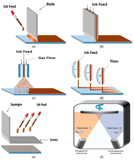
Figure 13.
Scalable deposition methods: (a) Doctor-blade coating; (b) Slot-die coating; (c) Spray coating; (d) Inkjet printing; (e) Screen printing; (f) Vapor-phase deposition [183].
5.3.2. Slot-Die Coating
Slot-die coating is similar to doctor-blade coating, and uses a die as ink reservoir to spread liquid through a slot (Figure 13b). Ink flow can be better controlled than doctor-blade coating, but this method normally requires larger quantities of ink to fill the ink reservoir and supply pipe and, thus, has been less explored and, at present, the PSCs prepared using a slot-die coating method have a much lower PCE than those fabricated through doctor-blade coating. However, the slot-die coating has been developed for many years, and is suitable for roll-to-roll deposition, which provides a better future for large-scale PSC fabrication [167,168,169]. Burkitt et al. achieved four slot-die coated layers including perovskite, HTL, ETL, and mesoporous layer, and the process is greatly simplified [170]. Kim et al. developed a single-step slot-die coating, and used gas quenching and substrate heating to achieve a defect-free dense perovskite layer, resulting in a PCE of 12.7% [171].
5.3.3. Spray Coating
Spray coating disperses tiny liquid droplets onto substrates through a nozzle (Figure 13c). According to different ways of dispersing the droplets, it can be further classified, such as pneumatic spraying (through fast gas flow), ultrasonic spraying (through ultrasonic vibration), or electrospraying (through electrical repulsion). Among these spray methods, ultrasonic spraying is commonly introduced to fabricate perovskite layer and ETL [172,173,174,175]. Several droplets need to overlap in a local area, in other words, multiple spraying needs to be carried out to ensure full coverage. The substrate should be kept at an elevated temperature during spraying, in order to increase the rate of solvent evaporation and suppress the redissolution of deposited material.
5.3.4. Inkjet Printing and Screen Printing
In inkjet printing process, nozzles with a piezo material are used to disperse the precursor ink, with fine control of the droplet size and pattern (Figure 13d). Inkjet printing can be applied to prepare mesoporous [176,177] and monolithic hole-conductor-free PSCs [178,179], which can be easily combined with a roll-to-roll process. Screen printing always needs a patterned mesh screen to hold and transfer ink to the substrate (Figure 13e). This method has good patterning ability, with a lateral resolution of around 75–100 µm [180]. Screen printing is usually used to deposit thicker films, thus, it is favored method to form mesoporous layers and carbon back electrodes [181,182].
5.3.5. Vapor-Phase Deposition
The vapor-phase method is common in solar cell fabrication, such as in the preparation of CuInGaSe2 (CIGS) and CdTe, which relies heavily on physical vapor deposition. Liu et al. employed vapor-phase method to the fabrication of perovskite film for the first time [183]. They use dual-source vapor deposition to create uniform flat films with high coverage, compared to films prepared through a solution process. The dual-source thermal evaporation system is shown in Figure 13f. Subsequently, a lot of reports combined solution-phase and vapor-phase method to form high-quality perovskite films without sophisticated vacuum equipment [184].
6. Summary and Future Outlook
PSCs have made great progress in the past nine years, thanks to the highlighted properties of organic–inorganic hybrid halide perovskite materials. Despite this rapid development, PSCs are still not comparable to other commercialized photovoltaics, such as crystalline silicon and CIGS, which we attributed to three aspects, and gave a detailed description. Firstly, there is still much room for improvement in the efficiency. Optimizing the chemical composition of the perovskite materials, introducing suitable additives to passivate the grain boundaries of the perovskite polycrystalline films, and modifying the interface by using some interlayers or passivator through interfacial engineering, can effectively improve the optoelectronic properties of perovskite materials and transportation of carriers in the interfaces, thereby enhancing the efficiency of PSCs. Secondly, the stability of PSCs has not been well solved. Moisture, oxygen, and thermal instability can be alleviated by adjusting the composition of the perovskite and, moreover, the application of low-dimensional perovskite materials is another solution toward these issues. Remarkably, the intrinsic moisture and oxygen problem can be overcome by application of some isolating layers and additives. The poor stability caused by UV light is generally due to the presence of TiO2, which can be settled by employing other kinds of ETL materials, and directly isolating the UV light. Finally, although perovskite has abundant low-cost raw materials, expensive organic hole transport materials and noble metals still make PSCs a high-cost photovoltaic device. For the HTL, inorganic materials can be an applicable replacement. The HTL can also be directly removed to fabricate hole-conductor-free PSCs. Regarding metal electrodes, a variety of carbon electrodes can be utilized to lower the cost of PSCs. When PSCs enter commercial large-scale production, a larger area of perovskite apparently increases productivity and reduces the cost of PSC modules. Therefore, we briefly overviewed common scalable deposition methods in which inkjet printing and screen printing represent well-developed technologies which can be easily introduced into a roll-to-roll process, making it the most promising method for large-scale production. PSCs can make a great step forward in commercialization on the condition that all the difficulties, described above, are completely resolved.
Author Contributions
All the authors participated in the completion of the article. Y.Z., X.Z. and L.W. conceived and designed the layout of the article. Y.S. and B.Z. conducted the literature collection and research. Y.Z. and H.Z. wrote the manuscript and supervised the whole study. G.H. and Y.L. reviewed the final paper.
Funding
This research was funded by National Natural Science Foundation of China, grant number 61274064.
Conflicts of Interest
The authors declare no conflict of interest.
References
- Kojima, A.; Teshima, K.; Shirai, Y.; Miyasaka, T. Organometal Halide Perovskites as Visible-Light Sensitizers for Photovoltaic Cells. J. Am. Chem. Soc. 2009, 131, 6050–6051. [Google Scholar] [CrossRef] [PubMed]
- Im, J.H.; Lee, C.R.; Lee, J.W.; Park, S.W.; Park, N.G. 6.5% Efficient Perovskite Quantum-Dot-Sensitized Solar Cell. Nanoscale 2011, 3, 4088–4093. [Google Scholar] [CrossRef] [PubMed]
- Kim, H.S.; Lee, C.R.; Im, J.H.; Lee, K.B.; Moehl, T.; Marchioro, A.; Moon, S.J.; Humphry-Baker, R.; Yum, J.H.; Moser, J.E.; et al. Lead Iodide Perovskite Sensitized All-Solid-State Submicron Thin Film Mesoscopic Solar Cell with Efficiency Exceeding 9%. Sci. Rep. 2012, 2, 591. [Google Scholar] [CrossRef] [PubMed]
- Lee, M.M.; Teuscher, J.; Miyasaka, T.; Murakami, T.N.; Snaith, H.J. Efficient Hybrid Solar Cells Based on Meso-Superstructured Organometal Halide Perovskites. Science 2012, 338, 643–647. [Google Scholar] [CrossRef] [PubMed]
- Yang, W.S.; Park, B.W.; Jung, E.H.; Jeon, N.J.; Kim, Y.C.; Lee, D.U.; Shin, S.S.; Seo, J.; Kim, E.K.; Noh, J.H.; et al. Iodide Management in Formamidinium-Lead-Halide-Based Perovskite Layers for Efficient Solar Cells. Science 2017, 356, 1376–1379. [Google Scholar] [CrossRef] [PubMed]
- NREL Chart. Available online: https://www.nrel.gov/pv/assets/pdfs/pv-efficiencies-07-17-2018.pdf (accessed on 17 July 2018).
- Ting, H.K.; Ni, L.; Ma, S.B.; Ma, Y.Z.; Xiao, L.X.; Chen, Z.J. Progress in Electron-Transport Materials in Application of Perovskite Solar Cells. Acta Phys. Sin. 2015, 64, 038802. [Google Scholar] [CrossRef]
- Ma, Y.Z.; Wang, S.F.; Zheng, L.L.; Lu, Z.L.; Zhang, D.F.; Bian, Z.Q.; Huang, C.H.; Xiao, L.X. Recent Research Developments of Perovskite Solar Cells. Chin. J. Chem. 2014, 32, 957–963. [Google Scholar] [CrossRef]
- De Wolf, S.; Holovsky, J.; Moon, S.J.; Loper, P.; Niesen, B.; Ledinsky, M.; Haug, F.J.; Yum, J.H.; Ballif, C. Organometallic Halide Perovskites: Sharp Optical Absorption Edge and Its Relation to Photovoltaic Performance. J. Phys. Chem. Lett. 2014, 5, 1035–1039. [Google Scholar] [CrossRef] [PubMed]
- Stranks, S.D.; Eperon, G.E.; Grancini, G.; Menelaou, C.; Alcocer, M.J.P.; Leijtens, T.; Herz, L.M.; Petrozza, A.; Snaith, H.J. Electron-Hole Diffusion Lengths Exceeding 1 Micrometer in An Organometal Trihalide Perovskite Absorber. Science 2013, 342, 341–344. [Google Scholar] [CrossRef] [PubMed]
- Valverde-Chavez, D.A.; Ponseca, C.S.; Stoumpos, C.C.; Yartsev, A.; Kanatzidis, M.G.; Sundstrom, V.; Cooke, D.G. Intrinsic Femtosecond Charge Generation Dynamics in Single Crystal CH3NH3PbI3. Energy Environ. Sci. 2015, 8, 3700–3707. [Google Scholar] [CrossRef]
- Miyata, A.; Mitioglu, A.; Plochocka, P.; Portugall, O.; Wang, J.T.W.; Stranks, S.D.; Snaith, H.J.; Nicholas, R.J. Direct Measurement of The Exciton Binding Energy and Effective Masses for Charge Carriers in Organic-Inorganic Tri-Halide Perovskites. Nat. Phys. 2015, 11, 582–588. [Google Scholar] [CrossRef]
- Ku, Z.L.; Rong, Y.G.; Xu, M.; Liu, T.F.; Han, H.W. Full Printable Processed Mesoscopic CH3NH3PbI3/TiO2 Heterojunction Solar Cells with Carbon Counter Electrode. Sci. Rep. 2013, 3, 3132. [Google Scholar] [CrossRef] [PubMed]
- Pellet, N.; Gao, P.; Gregori, G.; Yang, T.Y.; Nazeeruddin, M.K.; Maier, J.; Gratzel, M. Mixed-Organic-Cation Perovskite Photovoltaics for Enhanced Solar-Light Harvesting. Angew. Chem.-Int. Edit. 2014, 53, 3151–3157. [Google Scholar] [CrossRef] [PubMed]
- Yang, W.S.; Noh, J.H.; Jeon, N.J.; Kim, Y.C.; Ryu, S.; Seo, J.; Seok, S.I. High-Performance Photovoltaic Perovskite Layers Fabricated Through Intramolecular Exchange. Science 2015, 348, 1234–1237. [Google Scholar] [CrossRef] [PubMed]
- Ogomi, Y.; Morita, A.; Tsukamoto, S.; Saitho, T.; Fujikawa, N.; Shen, Q.; Toyoda, T.; Yoshino, K.; Pandey, S.S.; Ma, T.L.; et al. CH3NH3SnxPb(1−x)I3 Perovskite Solar Cells Covering up to 1060 nm. J. Phys. Chem. Lett. 2014, 5, 1004–1011. [Google Scholar] [CrossRef] [PubMed]
- Stoumpos, C.C.; Malliakas, C.D.; Kanatzidis, M.G. Semiconducting Tin and Lead Iodide Perovskites with Organic Cations: Phase Transitions, High Mobilities, and Near-infrared Photoluminescent Properties. Inorg. Chem. 2013, 52, 9019–9038. [Google Scholar] [CrossRef] [PubMed]
- Noh, J.H.; Im, S.H.; Heo, J.H.; Mandal, T.N.; Seok, S.I. Chemical Management for Colorful, Efficient, and Stable Inorganic-Organic Hybrid Nanostructured Solar Cells. Nano Lett. 2013, 13, 1764–1769. [Google Scholar] [CrossRef] [PubMed]
- Shockley, W.; Queisser, H.J. Detailed Balance Limit of Efficiency of p-n Junction Solar Cells. J. Appl. Phys. 1961, 32, 510–519. [Google Scholar] [CrossRef]
- Choi, H.; Jeong, J.; Kim, H.B.; Kim, S.; Walker, B.; Kim, G.H.; Kim, J.Y. Cesium-Doped Methylammonium Lead Iodide Perovskite Light Absorber for Hybrid Solar Cells. Nano Energy 2014, 7, 80–85. [Google Scholar] [CrossRef]
- Jeon, N.J.; Noh, J.H.; Yang, W.S.; Kim, Y.C.; Ryu, S.; Seo, J.; Seok, S.I. Compositional Engineering of Perovskite Materials for High-Performance Solar Cells. Nature 2015, 517, 476–480. [Google Scholar] [CrossRef] [PubMed]
- Li, Z.; Yang, M.J.; Park, J.S.; Wei, S.H.; Berry, J.J.; Zhu, K. Stabilizing Perovskite Structures by Tuning Tolerance Factor: Formation of Formamidinium and Cesium Lead Iodide Solid-State Alloys. Chem. Mat. 2015, 28, 284–292. [Google Scholar] [CrossRef]
- Lee, J.W.; Kim, D.H.; Kim, H.S.; Seo, S.W.; Cho, S.M.; Park, N.G. Formamidinium and Cesium Hybridization for Photo- and Moisture-Stable Perovskite Solar Cell. Adv. Energy Mater. 2015, 5, 1501310. [Google Scholar] [CrossRef]
- Yi, C.Y.; Luo, J.S.; Meloni, S.; Boziki, A.; Ashari-Astani, N.; Gratzel, C.; Zakeeruddin, S.M.; Rothlisberger, U.; Gratzel, M. Entropic Stabilization of Mixed A-Cation ABX3 Metal Halide Perovskites for High Performance Perovskite Solar Cells. Energy Environ. Sci. 2016, 9, 656–662. [Google Scholar] [CrossRef]
- Bi, D.Q.; Tress, W.; Dar, M.I.; Gao, P.; Luo, J.S.; Renevier, C.; Schenk, K.; Abate, A.; Giordano, F.; Baena, J.P.C.; et al. Efficient Luminescent Solar Cells Based on Tailored Mixed-Cation Perovskites. Sci. Adv. 2016, 2, e1501170. [Google Scholar] [CrossRef] [PubMed]
- Jeon, N.J.; Na, H.; Jung, E.H.; Yang, T.Y.; Lee, Y.G.; Kim, G.; Shin, H.W.; Seok, S.I.; Lee, J.; Seo, J. A Fluorene-Terminated Hole-Transporting Material for Highly Efficient and Stable Perovskite Solar Cells. Nat. Energy 2018, 3, 682–689. [Google Scholar] [CrossRef]
- Eperon, G.E.; Paterno, G.M.; Sutton, R.J.; Zampetti, A.; Haghighirad, A.A.; Cacialli, F.; Snaith, H.J. Inorganic Caesium Lead Iodide Perovskite Solar Cells. J. Mater. Chem. A 2015, 3, 19688–19695. [Google Scholar] [CrossRef]
- Saliba, M.; Matsui, T.; Seo, J.Y.; Domanski, K.; Correa-Baena, J.P.; Nazeeruddin, M.K.; Zakeeruddin, S.M.; Tress, W.; Abate, A.; Hagfeldt, A.; et al. Cesium-Containing Triple Cation Perovskite Solar Cells: Improved Stability, Reproducibility and High Efficiency. Energy Environ. Sci. 2016, 9, 1989–1997. [Google Scholar] [CrossRef] [PubMed]
- Peng, J.; Duong, T.; Zhou, X.Z.; Shen, H.P.; Wu, Y.L.; Mulmudi, H.K.; Wan, Y.M.; Zhong, D.Y.; Li, J.T.; Tsuzuki, T.; et al. Efficient Indium-Doped TiOx Electron Transport Layers for High-Performance Perovskite Solar Cells and Perovskite-Silicon Tandems. Adv. Energy Mater. 2016, 7, 1601768. [Google Scholar] [CrossRef]
- Saliba, M.; Matsui, T.; Domanski, K.; Seo, J.Y.; Ummadisingu, A.; Zakeeruddin, S.M.; Correa-Baena, J.P.; Tress, W.R.; Abate, A.; Hagfeldt, A.; et al. Incorporation of Rubidium Cations into Perovskite Solar Cells Improves Photovoltaic Performance. Science 2016, 354, 206–209. [Google Scholar] [CrossRef] [PubMed]
- Park, Y.H.; Jeong, I.; Bae, S.; Son, H.J.; Lee, P.; Lee, J.; Lee, C.H.; Ko, M.J. Inorganic Rubidium Cation as an Enhancer for Photovoltaic Performance and Moisture Stability of HC(NH2)2PbI3 Perovskite Solar Cells. Adv. Funct. Mater. 2017, 27, 1605988. [Google Scholar] [CrossRef]
- Hao, F.; Stoumpos, C.C.; Chang, R.P.H.; Kanatzidis, M.G. Anomalous Band Gap Behavior in Mixed Sn and Pb Perovskites Enables Broadening of Absorption Spectrum in Solar Cells. J. Am. Chem. Soc. 2014, 136, 8094–8099. [Google Scholar] [CrossRef] [PubMed]
- Kulkarni, S.A.; Baikie, T.; Boix, P.P.; Yantara, N.; Mathews, N.; Mhaisalkar, S. Band-Gap Tuning of Lead Halide Perovskites Using a Sequential Deposition Process. J. Mater. Chem. A 2014, 2, 9221–9225. [Google Scholar] [CrossRef]
- Rohatgi, A.; Kim, D.S.; Nakayashiki, K.; Yelundur, V.; Rounsaville, B. High-Efficiency Solar Cells on Edge-Defined Film-Fed Grown (18.2%) and String Ribbon (17.8%) Silicon by Rapid Thermal Processing. Appl. Phys. Lett. 2004, 84, 145–147. [Google Scholar] [CrossRef]
- Yan, Y.F.; Yin, W.J.; Wu, Y.L.; Shi, T.T.; Paudel, N.R.; Li, C.; Poplawsky, J.; Wang, Z.W.; Moseley, J.; Guthrey, H.; et al. Physics of Grain Boundaries in Polycrystalline Photovoltaic Semiconductors. J. Appl. Phys. 2015, 117, 112807. [Google Scholar] [CrossRef]
- Yan, Y.; Jiang, C.S.; Noufi, R.; Wei, S.H.; Moutinho, H.R.; Al-Jassim, MM. Electrically Benign Behavior of Grain Boundaries in Polycrystalline CuInSe2, Films. Phys. Rev. Lett. 2007, 99, 235504. [Google Scholar] [CrossRef] [PubMed]
- Guo, Y.G.; Wang, Q.; Saidi, W.A. Structural Stabilities and Electronic Properties of High-Angle Grain Boundaries in Perovskite Cesium Lead Halides. J. Phys. Chem. C 2017, 121, 1715–1722. [Google Scholar] [CrossRef]
- Lee, J.W.; Park, N.G. Two-Step Deposition Method for High-Efficiency Perovskite Solar Cells. MRS Bull. 2015, 40, 654–659. [Google Scholar] [CrossRef]
- Roldan-Carmona, C.; Gratia, P.; Zimmermann, I.; Grancini, G.; Gao, P.; Graetzel, M.; Nazeeruddin, M.K. High Efficiency Methylammonium Lead Triiodide Perovskite Solar Cells: The Relevance of Non-Stoichiometric Precursors. Energy Environ. Sci. 2015, 8, 3550–3556. [Google Scholar] [CrossRef]
- Kim, Y.C.; Jeon, N.J.; Noh, J.H.; Yang, W.S.; Seo, J.; Yun, J.S.; Ho-Baillie, A.; Huang, S.J.; Green, M.A.; Seidel, J.; et al. Beneficial Effects of PbI2 Incorporated in Organo-Lead Halide Perovskite Solar Cells. Adv. Energy Mater. 2016, 6, 1502104. [Google Scholar] [CrossRef]
- Wang, H.Y.; Hao, M.Y.; Han, J.; Yu, M.; Qin, Y.J.; Zhang, P.; Guo, Z.X.; Ai, X.C.; Zhang, J.P. The Adverse Effects of Excessively Remained PbI2 on Photovoltaic Performance, Charge Separation and Trap State Properties in Mesoporous Structured Perovskite Solar Cells. Chem.-Eur. J. 2017, 23, 3986–3992. [Google Scholar] [CrossRef] [PubMed]
- Hsu, H.Y.; Ji, L.; Du, M.S.; Zhao, J.; Yu, E.T.; Bard, A.J. Optimization of PbI2/MAPbI3 Perovskite Composites by Scanning Electrochemical Microscopy. J. Phys. Chem. C 2016, 120, 19890–19895. [Google Scholar] [CrossRef]
- Son, D.Y.; Lee, J.W.; Choi, Y.J.; Jang, I.H.; Lee, S.; Yoo, P.J.; Shin, H.; Ahn, N.; Choi, M.; Kim, D.; et al. Self-Formed Grain Boundary Healing Layer for Highly Efficient CH3NH3PbI3 Perovskite Solar Cells. Nat. Energy 2016, 67, 16081. [Google Scholar] [CrossRef]
- Li, X.; Bi, D.Q.; Yi, C.Y.; Decoppet, J.D.; Luo, J.S.; Zakeeruddin, S.M.; Hagfeldt, A.; Gratzel, M. A Vacuum Flash-Assisted Solution Process for High-Efficiency Large-Area Perovskite Solar Cells. Science 2016, 353, 58–62. [Google Scholar] [CrossRef] [PubMed]
- Saliba, M.; Orlandi, S.; Matsui, T.; Aghazada, S.; Cavazzini, M.; Correa-Baena, J.P.; Gao, P.; Scopelliti, R.; Mosconi, E.; Dahmen, K.H.; et al. A Molecularly Engineered Hole-Transporting Material for Efficient Perovskite Solar Cells. Nat. Energy 2016, 1, 15017. [Google Scholar] [CrossRef]
- Zheng, Y.Z.; Li, X.T.; Zhao, E.F.; Lv, X.D.; Meng, F.L.; Peng, C.; Lai, X.S.; Huang, M.L.; Cao, G.Z.; Tao, X.; et al. Hexamethylenetetramine-Mediated Growth of Grain-Boundary-Passivation CH3NH3PbI3 for Highly Reproducible and Stable Perovskite Solar Cells. J. Power Sources 2017, 377, 103–109. [Google Scholar] [CrossRef]
- Tong, Y.H.; Liu, Y.C.; Dong, L.; Zhao, D.X.; Zhang, J.Y.; Lu, Y.M.; Shen, D.Z.; Fan, X.W. Growth of ZnO Nanostructures with Different Morphologies by Using Hydrothermal Technique. J. Phys. Chem. B 2006, 110, 20263–20267. [Google Scholar] [CrossRef] [PubMed]
- Li, X.; Chen, C.C.; Cai, M.L.; Hua, X.; Xie, F.X.; Liu, X.; Hua, J.L.; Long, Y.T.; Tian, H.; Han, L.Y. Efficient Passivation of Hybrid Perovskite Solar Cells Using Organic Dyes with -COOH Functional Group. Adv. Energy Mater. 2018, 8, 1800715. [Google Scholar] [CrossRef]
- Ooyama, Y.; Harima, Y. Photophysical and Electrochemical Properties, and Molecular Structures of Organic Dyes for Dye-Sensitized Solar Cells. ChemPhysChem 2013, 13, 4032–4080. [Google Scholar] [CrossRef] [PubMed]
- Park, C.; Ko, H.; Sin, D.H.; Song, K.C.; Cho, K. Organometal Halide Perovskite Solar Cells with Improved Thermal Stability via Grain Boundary Passivation Using a Molecular Additive. Adv. Funct. Mater. 2017, 27, 1703546. [Google Scholar] [CrossRef]
- Lee, D.; Yun, J.S.; Kim, J.; Soufiani, A.M.; Chen, S.; Cho, Y.; Deng, X.F.; Seidel, J.; Lim, S.; Huang, S.J.; et al. Passivation of Grain Boundaries by Phenethylammonium in Formamidinium-Methylammonium Lead Halide Perovskite Solar Cells. ACS Energy Lett. 2018, 3, 647–654. [Google Scholar] [CrossRef]
- Wang, Y.F.; Zhang, J.; Chen, S.H.; Zhang, H.Y.; Li, L.G.; Fu, Z.Y. Surface Passivation with Nitrogen-Doped Carbon Dots for Improved Perovskite Solar Cell Performance. J. Mater. Sci. 2018, 53, 9180–9190. [Google Scholar] [CrossRef]
- Liu, L.F.; Mei, A.Y.; Liu, T.F.; Jiang, P.; Sheng, Y.S.; Zhang, L.J.; Han, H.W. Fully Printable Mesoscopic Perovskite Solar Cells with Organic Silane Self-Assembled Monolayer. J. Am. Chem. Soc. 2015, 137, 1790–1793. [Google Scholar] [CrossRef] [PubMed]
- Rao, S.S.; Punnoose, D.; Tulasivarma, C.V.; Kumar, C.H.S.S.P.; Gopi, C.V.V.M.; Kim, S.K.; Kim, H.J. A Strategy to Enhance the Efficiency of Dye-Sensitized Solar Cells by the Highly Efficient TiO2/ZnS Photoanode. Dalton Trans. 2015, 44, 2447–2455. [Google Scholar] [CrossRef]
- Wang, Y.; Mahmoudi, T.; Rho, W.Y.; Yang, H.Y.; Seo, S.; Bhat, K.S.; Ahmad, R.; Hahn, Y.B. Ambient-Air-Solution-Processed Efficient and Highly Stable Perovskite Solar Cells Based on CH3NH3PbI3−xClx-NiO Composite with Al2O3/NiO Interfacial Engineering. Nano Energy 2017, 40, 408–417. [Google Scholar] [CrossRef]
- Shaikh, S.F.; Kwon, H.C.; Yang, W.; Mane, R.S.; Moon, J. Performance Enhancement of Mesoporous TiO2-Based Perovskite Solar Cells by ZnS Ultrathin-Interfacial Modification Layer. J. Alloys Compd. 2017, 738, 405–414. [Google Scholar] [CrossRef]
- Wang, Y.Q.; Xu, S.B.; Deng, J.G.; Gao, L.Z. Enhancing the Efficiency of Planar Heterojunction Perovskite Solar Cells via Interfacial Engineering with 3-aminopropyl Trimethoxy Silane Hydrolysate. R. Soc. Open Sci. 2017, 4, 170980. [Google Scholar] [CrossRef] [PubMed]
- Lu, J.F.; Lin, X.F.; Jiao, X.C.; Gengenbach, T.; Scully, A.D.; Jiang, L.C.; Tan, B.; Sun, J.S.; Li, B.; Pai, N.; et al. Interfacial Benzenethiol Modification Facilitates Charge Transfer and Improves Stability of cm-sized Metal Halide Perovskite Solar Cells with up to 20% Efficiency. Energy Environ. Sci. 2018, 11, 1880–1889. [Google Scholar] [CrossRef]
- Wang, F.J.; Shirnazaki, A.; Yang, F.J.; Kanahashi, K.; Matsuldi, K.; Miyauchi, Y.; Takenobu, T.; Wakamiya, A.; Murata, Y.; Matsuda, K. Highly Efficient and Stable Perovskite Solar Cells by Interfacial Engineering Using Solution-Processed Polymer Layer. J. Phys. Chem. C 2017, 121, 1562–1568. [Google Scholar] [CrossRef]
- Singh, T.; Oz, S.; Sasinska, A.; Frohnhoven, R.; Mathur, S.; Miyasaka, T. Sulfate-Assisted Interfacial Engineering for High Yield and Efficiency of Triple Cation Perovskite Solar Cells with Alkali-Doped TiO2 Electron-Transporting Layers. Adv. Funct. Mater. 2018, 28, 1706287. [Google Scholar] [CrossRef]
- Zheng, L.Y.; Mukherjee, S.; Wang, K.; Hay, M.E.; Boudouris, B.W.; Gong, X. Radical Polymers as Interfacial Layers in Inverted Hybrid Perovskite Solar Cells. J. Mater. Chem. A 2017, 5, 23831–23839. [Google Scholar] [CrossRef]
- Lee, J.; Kang, H.; Kim, G.; Back, H.; Kim, J.; Hong, S.; Park, B.; Lee, E.; Lee, K. Achieving Large-Area Planar Perovskite Solar Cells by Introducing an Interfacial Compatibilizer. Adv. Mater. 2017, 29, 1606363. [Google Scholar] [CrossRef] [PubMed]
- Grancini, G.; Roldan-Carmona, C.; Zimmermann, I.; Mosconi, E.; Lee, X.; Martineau, D.; Narbey, S.; Oswald, F.; De Angelis, F.; Graetzel, M.; et al. One-Year Stable Perovskite Solar Cells by 2D/3D Interface Engineering. Nat. Commun. 2017, 8, 15684. [Google Scholar] [CrossRef] [PubMed]
- Niu, G.D.; Guo, X.D.; Wang, L.D. Review of Recent Progress in Chemical Stability of Perovskite Solar Cells. J. Mater. Chem. A 2014, 3, 8970–8980. [Google Scholar] [CrossRef]
- O’Mahony, F.T.F.; Lee, Y.H.; Jellett, C.; Dmitrov, S.; Bryant, D.T.J.; Durrant, J.R.; O’Regan, B.C.; Graetzel, M.; Nazeeruddin, M.K.; Haque, S.A. Improved Environmental Stability of Organic Lead Trihalide Perovskite-Based Photoactive-Layers in the Presence of Mesoporous TiO2. J. Mater. Chem. A 2015, 3, 7219–7223. [Google Scholar] [CrossRef]
- Jeon, N.J.; Noh, J.H.; Kim, Y.C.; Yang, W.S.; Ryu, S.; Seok, S.I. Solvent Engineering for High-Performance Inorganic-Organic Hybrid Perovskite Solar Cells. Nat. Mater. 2014, 13, 897–903. [Google Scholar] [CrossRef] [PubMed]
- Zhu, W.D.; Bao, C.X.; Li, F.M.; Yu, T.; Gao, H.; Yi, Y.; Yang, J.; Fu, G.; Zhou, X.X.; Zou, Z.G. A Halide Exchange Engineering for CH3NH3PbI3−xBrx, Perovskite Solar Cells with High Performance and Stability. Nano Energy 2016, 19, 17–26. [Google Scholar] [CrossRef]
- Hoke, E.T.; Slotcavage, D.J.; Dohner, E.R.; Bowring, A.R.; Karunadasa, H.I.; McGehee, M.D. Reversible Photo-Induced Trap Formation in Mixed-Halide Hybrid Perovskites for Photovoltaics. Chem. Sci. 2014, 6, 613–617. [Google Scholar] [CrossRef] [PubMed]
- Conings, B.; Drijkoningen, J.; Gauquelin, N.; Babayigit, A.; D’Haen, J.; D’Olieslaeger, L.; Ethirajan, A.; Verbeeck, J.; Manca, J.; Mosconi, E.; et al. Intrinsic Thermal Instability of Methylammonium Lead Trihalide Perovskite. Adv. Energy Mater. 2015, 5, 1500477. [Google Scholar] [CrossRef]
- Lee, J.W.; Seol, D.J.; Cho, A.N.; Park, N.G. High-Efficiency Perovskite Solar Cells Based on the Black Polymorph of HC(NH2)2 PbI3. Adv. Mater. 2014, 26, 4991–4998. [Google Scholar] [CrossRef] [PubMed]
- Liang, J.; Wang, C.X.; Wang, Y.R.; Xu, Z.R.; Lu, Z.P.; Ma, Y.; Zhu, H.F.; Hu, Y.; Xiao, C.C.; Yi, X.; et al. All-Inorganic Perovskite Solar Cells. J. Am. Chem. Soc. 2016, 138, 15829–15832. [Google Scholar] [CrossRef] [PubMed]
- Frolova, L.A.; Anokhin, D.V.; Piryazev, A.A.; Luchkin, S.Y.; Dremova, N.N.; Stevenson, K.J.; Troshin, P.A. Highly Efficient All-Inorganic Planar Heterojunction Perovskite Solar Cells Produced by Thermal Coevaporation of CsI and PbI2. J. Phys. Chem. Lett. 2016, 8, 67–72. [Google Scholar] [CrossRef] [PubMed]
- Wang, Q.; Dong, Q.F.; Li, T.; Gruverman, A.; Huang, J.S. Thin Insulating Tunneling Contacts for Efficient and Water-Resistant Perovskite Solar Cells. Adv. Mater. 2016, 28, 6734–6739. [Google Scholar] [CrossRef] [PubMed]
- Chen, W.; Xu, L.M.; Feng, X.Y.; Jie, J.S.; He, Z. Metal Acetylacetonate Series in Interface Engineering for Full Low-Temperature-Processed, High-Performance, and Stable Planar Perovskite Solar Cells with Conversion Efficiency over 16% on 1 cm2 Scale. Adv. Mater. 2017, 29, 1603923. [Google Scholar] [CrossRef] [PubMed]
- Wang, F.; Geng, W.; Zhou, Y.; Fang, H.H.; Tong, C.J.; Loi, M.A.; Liu, L.M.; Zhao, N. Phenylalkylamine Passivation of Organolead Halide Perovskites Enabling High-Efficiency and Air-Stable Photovoltaic Cells. Adv. Mater. 2016, 28, 9986–9992. [Google Scholar] [CrossRef] [PubMed]
- Xu, J.X.; Voznyy, O.; Comin, R.; Gong, X.W.; Walters, G.; Liu, M.; Kanjanaboos, P.; Lan, X.Z.; Sargent, E.H. Crosslinked Remote-Doped Hole-Extracting Contacts Enhance Stability under Accelerated Lifetime Testing in Perovskite Solar Cells. Adv. Mater. 2016, 28, 2807–2815. [Google Scholar] [CrossRef] [PubMed]
- Pisoni, A.; Jacimovic, J.; Barisic, O.S.; Spina, M.; Gaal, R.; Forro, L.; Horvath, E. Ultra-Low Thermal Conductivity in Organic-Inorganic Hybrid Perovskite CH3NH3PbI3. J. Phys. Chem. Lett. 2014, 5, 2488–2492. [Google Scholar] [CrossRef] [PubMed]
- Beal, R.E.; Slotcavage, D.J.; Leijtens, T.; Bowring, A.R.; Belisle, R.A.; Nguyen, W.H.; Burkhard, G.F.; Hoke, E.T.; McGehee, M.D. Cesium Lead Halide Perovskites with Improved Stability for Tandem Solar Cells. J. Phys. Chem. Lett. 2016, 7, 746–751. [Google Scholar] [CrossRef] [PubMed]
- Eperon, G.E.; Stranks, S.D.; Menelaou, C.; Johnston, M.B.; Herz, L.M.; Snaith, H.J. Formamidinium Lead Trihalide: A Broadly Tunable Perovskite for Efficient Planar Heterojunction Solar Cells. Energy Environ. Sci. 2014, 7, 982–988. [Google Scholar] [CrossRef]
- McMeekin, D.P.; Sadoughi, G.; Rehman, W.; Eperon, G.E.; Saliba, M.; Horantner, M.T.; Haghighirad, A.; Sakai, N.; Korte, L.; Rech, B.; et al. A Mixed-Cation Lead Mixed-Halide Perovskite Absorber for Tandem Solar Cells. Science 2016, 351, 151–155. [Google Scholar] [CrossRef] [PubMed]
- Baikie, T.; Fang, Y.N.; Kadro, J.M.; Schreyer, M.; Wei, F.X.; Mhaisalkar, S.G.; Graetzel, M.; White, T.J. Synthesis and Crystal Chemistry of the Hybrid Perovskite CH3NH3PbI3 for Solid-State Sensitised Solar Cell Applications. J. Mater. Chem. A 2013, 1, 5628–5641. [Google Scholar] [CrossRef]
- Swarnkar, A.; Marshall, A.R.; Sanehira, E.M.; Chernomordik, B.D.; Moore, D.T.; Christians, J.A.; Chakrabarti, T.; Luther, J.M. Quantum Dot-Induced Phase Stabilization of α-CsPbI3 Perovskite for High-Efficiency Photovoltaics. Science 2016, 354, 92–95. [Google Scholar] [CrossRef] [PubMed]
- Malinauskas, T.; Tomkute-Luksiene, D.; Sens, R.; Daskeviciene, M.; Send, R.; Wonneberger, H.; Jankauskas, V.; Bruder, I.; Getautis, V. Enhancing Thermal Stability and Lifetime of Solid-State Dye-Sensitized Solar Cells via Molecular Engineering of the Hole Transporting Material spiro-OMeTAD. ACS Appl. Mater. Interfaces 2015, 7, 11107–11116. [Google Scholar] [CrossRef] [PubMed]
- Li, W.Z.; Dong, H.P.; Wang, L.D.; Li, N.; Guo, X.D.; Li, J.W.; Qiu, Y. Montmorillonite as Bifunctional Buffer Layer Material for Hybrid Perovskite Solar Cells with Protection from Corrosion and Retarding Recombination. J. Mater. Chem. A 2014, 2, 13587–13592. [Google Scholar] [CrossRef]
- Zhang, J.B.; Zhang, T.; Jiang, L.C.; Bach, U.; Cheng, Y.B. 4-tert-Butylpyridine Free Hole Transport Materials for Efficient Perovskite Solar Cells: A New Strategy to Enhance the Environmental and Thermal Stability. ACS Energy Lett. 2018, 3, 1677–1682. [Google Scholar] [CrossRef]
- Zhao, X.; Kim, H.S.; Seo, J.Y.; Park, N.G. Effect of Selective Contacts on the Thermal Stability of Perovskite Solar Cells. ACS Appl. Mater. Interfaces 2017, 9, 7148–7153. [Google Scholar] [CrossRef] [PubMed]
- Quan, L.N.; Yuan, M.J.; Comin, R.; Voznyy, O.; Beauregard, E.M.; Hoogland, S.; Buin, A.; Kirmani, A.R.; Zhao, K.; Amassian, A.; et al. Ligand-Stabilized Reduced-Dimensionality Perovskites. J. Am. Chem. Soc. 2016, 138, 2649–2655. [Google Scholar] [CrossRef] [PubMed]
- Peng, W.; Yin, J.; Ho, K.T.; Ouellette, O.; De Bastiani, M.; Murali, B.; El Tall, O.; Shen, C.; Miao, X.H.; Pan, J.; et al. Ultralow Self-Doping in 2D Hybrid Perovskite Single Crystals. Nano Lett. 2017, 17, 4759–4767. [Google Scholar] [CrossRef] [PubMed]
- Lin, Y.; Bai, Y.; Fang, Y.J.; Wang, Q.; Deng, Y.H.; Huang, J.S. Suppressed Ion Migration in Low Dimensional Perovskites. ACS Energy Lett. 2017, 2, 1571–1572. [Google Scholar] [CrossRef]
- Mitzi, D.B. Templating and Structural Engineering in Organic–Inorganic Perovskites. J. Chem. Soc. Dalton 2000, 1, 1–12. [Google Scholar] [CrossRef]
- Kamminga, M.E.; Fang, H.H.; Filip, M.R.; Giustino, F.; Baas, J.; Blake, G.R.; Loi, M.A.; Palstra, T.T.M. Confinement Effects in Low-Dimensional Lead Iodide Perovskite Hybrids. Chem. Mater. 2016, 28, 4554–4562. [Google Scholar] [CrossRef]
- Muljarov, E.A.; Tikhodeev, S.G.; Gippius, N.A. Excitons in Self-Organized Semiconductor/Insulator Superlattices: PbI-Based Perovskite Compounds. Phys. Rev. B 1995, 51, 14370–14378. [Google Scholar] [CrossRef]
- Smith, I.C.; Hoke, E.T.; Solis-Ibarra, D.; McGehee, M.D.; Karunadasa, H.I. A Layered Hybrid Perovskite Solar-Cell Absorber with Enhanced Moisture Stability. Angew. Chem.-Int. Ed. 2015, 126, 11232–11235. [Google Scholar] [CrossRef]
- Shayegan, Z.; Lee, C.S.; Haghighat, F. TiO2 Photocatalyst for Removal of Volatile Organic Compounds in Gas Phase—A Review. Chem. Eng. J. 2018, 334, 2408–2439. [Google Scholar] [CrossRef]
- Leijtens, T.; Eperon, G.E.; Pathak, S.; Abate, A.; Lee, M.M.; Snaith, H.J. Overcoming Ultraviolet Light Instability of Sensitized TiO2 with Meso-Superstructured Organometal Tri-Halide Perovskite Solar Cells. Nat. Commun. 2013, 4, 2885. [Google Scholar] [CrossRef] [PubMed]
- Ito, S.; Tanaka, S.; Manabe, K.; Nishino, H. Effects of Surface Blocking Layer of Sb2S3 on Nanocrystalline TiO2 for CH3NH3PbI3 Perovskite Solar Cells. J. Phys. Chem. C 2014, 118, 16995–17000. [Google Scholar] [CrossRef]
- Roose, B.; Johansen, C.M.; Dupraz, K.; Jaouen, T.; Aebi, P.; Steiner, U.; Abate, A. Ga-Doped SnO2 Mesoporous Contact for UV Stable Highly Efficient Perovskite Solar Cells. J. Mater. Chem. A 2017, 6, 1850–1857. [Google Scholar] [CrossRef]
- Yin, G.N.; Zhao, H.; Feng, J.S.; Sun, J.; Yan, J.Q.; Liu, Z.K.; Lin, S.H.; Liu, S.Z. A Low-Temperature and Facile Solution-Processed Two-Dimensional TiS2 as an Effective Electron Transport Layer for UV-Stable Planar Perovskite solar cell. J. Mater. Chem. A 2018, 6, 9132–9138. [Google Scholar] [CrossRef]
- Tsai, C.H.; Li, N.; Lee, C.C.; Wu, H.C.; Zhu, Z.L.; Wang, L.D.; Chen, W.C.; Yan, H.; Chueh, C.C. Efficient and UV-Stable Perovskite Solar Cells Enabled by Side Chain-Engineered Polymeric Hole-Transporting Layers. J. Mater. Chem. A 2018, 6, 12999–13004. [Google Scholar] [CrossRef]
- Cao, J.; Lv, X.D.; Zhang, P.; Chuong, T.T.; Wu, B.H.; Feng, X.X.; Shan, C.F.; Liu, J.C.; Tang, Y. Plant Sunscreen and Co(II)/(III) Porphyrins for UV-Resistant and Thermally Stable Perovskite Solar Cells: From Natural to Artificial. Adv. Mater. 2018, 30, 1800568. [Google Scholar] [CrossRef] [PubMed]
- Roh, H.S.; Han, G.S.; Lee, S.; Kim, S.; Choi, S.; Yoon, C.; Lee, J.K. New Down-Converter for UV-Stable Perovskite Solar Cells: Phosphor-in-Glass. J. Power Sources 2018, 389, 135–139. [Google Scholar] [CrossRef]
- Heo, J.H.; Im, S.H.; Noh, J.H.; Mandal, T.N.; Lim, C.S.; Chang, J.A.; Lee, Y.H.; Kim, H.J.; Sarkar, A.; Nazeeruddin, M.K.; et al. Efficient Inorganic-Organic Hybrid Heterojunction Solar Cells Containing Perovskite Compound and Polymeric Hole Conductors. Nat. Photonics 2013, 7, 487–492. [Google Scholar] [CrossRef]
- Wang, H.; Liu, G.H.; Li, X.; Xiang, P.; Ku, Z.L.; Rong, Y.G.; Xu, M.; Liu, L.F.; Hu, M.; Yang, Y.; et al. Highly Efficient poly(3-hexylthiophene) Based Monolithic Dye-Sensitized Solar Cells with Carbon Counter Electrode. Energy Environ. Sci. 2011, 4, 2025–2029. [Google Scholar] [CrossRef]
- Maniarasu, S.; Korukonda, T.B.; Manjunath, V.; Ramasamy, E.; Ramesh, M.; Veerappan, G. Recent Advancement in Metal Cathode and Hole-Conductor-Free Perovskite Solar Cells for Low-Cost and High Stability: A Route Towards Commercialization. Renew. Sustain. Energy Rev. 2018, 82, 845–857. [Google Scholar] [CrossRef]
- Sun, W.H.; Ye, S.Y.; Rao, H.X.; Li, Y.L.; Liu, Z.W.; Xiao, L.X.; Chen, Z.J.; Bian, Z.Q.; Huang, C.H. Room-Temperature and Solution-Processed Copper Iodide as the Hole Transport Layer for Inverted Planar Perovskite Solar Cells. Nanoscale 2016, 8, 15954–15960. [Google Scholar] [CrossRef] [PubMed]
- Ye, S.Y.; Rao, H.X.; Yan, W.B.; Li, Y.L.; Sun, W.H.; Peng, H.T.; Liu, Z.W.; Bian, Z.Q.; Li, Y.F.; Huang, C.H. A Strategy to Simplify the Preparation Process of Perovskite Solar Cells by Co-deposition of a Hole-Conductor and a Perovskite Layer. Adv. Mater. 2016, 28, 9648–9654. [Google Scholar] [CrossRef] [PubMed]
- Liu, Z.H.; Zhu, A.L.; Cai, F.S.; Tao, L.M.; Zhou, Y.H.; Zhao, Z.X.; Chen, Q.; Cheng, Y.B.; Zhou, H.P. Nickel Oxide Nanoparticles for Efficient Hole Transport in p-i-n and n-i-p Perovskite Solar Cells. J. Mater. Chem. A 2017, 5, 6597–6605. [Google Scholar] [CrossRef]
- Kwon, U.; Kim, B.G.; Nguyen, D.C.; Park, J.H.; Ha, N.Y.; Kim, S.J.; Ko, S.H.; Lee, S.; Lee, D.; Park, H.J. Solution-Processible Crystalline NiO Nanoparticles for High-Performance Planar Perovskite Photovoltaic Cells. Sci. Rep. 2016, 6, 30759. [Google Scholar] [CrossRef] [PubMed]
- Zhu, Z.L.; Bai, Y.; Zhang, T.; Liu, Z.K.; Long, X.; Wei, Z.H.; Wang, Z.L.; Zhang, L.X.; Wang, J.N.; Yan, F.; et al. High-Performance Hole-Extraction Layer of Sol-Gel-Processed NiO Nanocrystals for Inverted Planar Perovskite Solar Cells. Angew. Chem.-Int. Ed. 2015, 53, 12571–12575. [Google Scholar] [CrossRef]
- Cui, J.; Meng, F.P.; Zhang, H.; Cao, K.; Yuan, H.L.; Cheng, Y.B.; Huang, F.; Wang, M.K. CH3NH3PbI3-Based Planar Solar Cells with Magnetron Sputtered Nickel Oxide. ACS Appl. Mater. Interfaces 2014, 6, 22862–22870. [Google Scholar] [CrossRef] [PubMed]
- Vivo, P.; Salunke, J.K.; Priimagi, A. Hole-Transporting Materials for Printable Perovskite Solar Cells. Materials 2017, 10, 1087. [Google Scholar] [CrossRef] [PubMed]
- Giorgi, G.; Yamashita, K. Organic-Inorganic Halide Perovskites: An Ambipolar Class of Materials with Enhanced Photovoltaic Performances. J. Mater. Chem. A 2015, 3, 8981–8991. [Google Scholar] [CrossRef]
- Stamplecoskie, K.G.; Manser, J.S.; Kamat, P.V. Dual Nature of the Excited State in Organic-Inorganic Lead Halide Perovskites. Energy Environ. Sci. 2014, 8, 208–215. [Google Scholar] [CrossRef]
- Edri, E.; Kirmayer, S.; Mukhopadhyay, S.; Gartsman, K.; Hodes, G.; Cahen, D. Elucidating the Charge Carrier Separation and Working Mechanism of CH3NH3PbI3−xClx Perovskite Solar Cells. Nat. Commun. 2014, 5, 3461. [Google Scholar] [CrossRef] [PubMed]
- Xing, G.C.; Mathews, N.; Sun, S.Y.; Lim, S.S.; Lam, Y.M.; Gratzel, M.; Mhaisalkar, S.; Sum, T.C. Long-Range Balanced Electron- and Hole-Transport Lengths in Organic-Inorganic CH3NH3PbI3. Science 2013, 342, 344–347. [Google Scholar] [CrossRef] [PubMed]
- Li, Y.; Yan, W.B.; Li, Y.L.; Wang, S.F.; Wang, W.; Bian, Z.Q.; Xiao, L.X.; Gong, Q.H. Direct Observation of Long Electron-Hole Diffusion Distance in CH3NH3PbI3 Perovskite Thin Film. Sci. Rep. 2015, 5, 14485. [Google Scholar] [CrossRef] [PubMed]
- Etgar, L.; Gao, P.; Xue, Z.S.; Peng, Q.; Chandiran, A.K.; Liu, B.; Nazeeruddin, M.K.; Gratzel, M. Mesoscopic CH3NH3PbI3/TiO2 Heterojunction Solar Cells. J. Am. Chem. Soc. 2012, 134, 17396–17399. [Google Scholar] [CrossRef] [PubMed]
- Aharon, S.; Gamliel, S.; El Cohen, B.; Etgar, L. Depletion Region Effect of Highly Efficient Hole Conductor Free CH3NH3PbI3 Perovskite Solar Cells. Phys. Chem. Chem. Phys. 2014, 16, 10512–10518. [Google Scholar] [CrossRef] [PubMed]
- Ma, Q.S.; Huang, S.J.; Wen, X.M.; Green, M.A.; Ho-Baillie, A.W.Y. Hole Transport Layer Free Inorganic CsPbIBr2 Perovskite Solar Cell by Dual Source Thermal Evaporation. Adv. Energy Mater. 2016, 6, 1502202. [Google Scholar] [CrossRef]
- Shi, J.J.; Luo, Y.H.; Wei, H.Y.; Luo, J.H.; Dong, J.; Lv, S.T.; Xiao, J.Y.; Xu, Y.Z.; Zhu, L.F.; Xu, X.; et al. Modified Two-Step Deposition Method for High-Efficiency TiO2/CH3NH3PbI3 Heterojunction Solar Cells. ACS Appl. Mater. Interfaces 2014, 6, 9711–9718. [Google Scholar] [CrossRef] [PubMed]
- Wei, H.Y.; Shi, J.J.; Xu, X.; Xiao, J.Y.; Luo, J.H.; Dong, J.; Lv, S.T.; Zhu, L.F.; Wu, H.J.; Li, D.M.; et al. Enhanced Charge Collection with Ultrathin AlOx Electron Blocking Layer for Hole-Transporting Material-Free Perovskite Solar Cell. Phys. Chem. Chem. Phys. 2015, 17, 4937–4944. [Google Scholar] [CrossRef] [PubMed]
- Xu, Y.Z.; Shi, J.J.; Lv, S.T.; Zhu, L.F.; Dong, J.; Wu, H.J.; Xiao, Y.; Luo, Y.H.; Wang, S.R.; Li, D.M.; et al. Simple Way to Engineer Metal-Semiconductor Interface for Enhanced Performance of Perovskite Organic Lead Iodide Solar Cells. ACS Appl. Mater. Interfaces 2014, 6, 5651–5656. [Google Scholar] [CrossRef] [PubMed]
- Zhang, F.Q.; Yang, X.C.; Wang, H.X.; Cheng, M.; Zhao, J.H.; Sun, L.C. Structure Engineering of Hole-Conductor Free Perovskite-Based Solar Cells with Low-Temperature-Processed Commercial Carbon Paste as Cathode. ACS Appl. Mater. Interfaces 2014, 6, 16140–16146. [Google Scholar] [CrossRef] [PubMed]
- Zhang, H.; Wang, H.; Williams, S.T.; Xiong, D.H.; Zhang, W.J.; Chueh, C.C.; Chen, W.; Jen, A.K.Y. SrCl2 Derived Perovskite Facilitating a High Efficiency of 16% in Hole-Conductor-Free Fully Printable Mesoscopic Perovskite Solar Cells. Adv. Mater. 2017, 29, 1606608. [Google Scholar] [CrossRef] [PubMed]
- Qiu, L.B.; Deng, J.; Lu, X.; Yang, Z.B.; Peng, H.S. Integrating Perovskite Solar Cells into a Flexible Fiber. Angew. Chem.-Int. Ed. 2015, 53, 10425–10428. [Google Scholar] [CrossRef] [PubMed]
- Li, Z.; Kulkarni, S.A.; Boix, P.P.; Shi, E.Z.; Cao, A.Y.; Fu, K.W.; Batabyal, S.K.; Zhang, J.; Xiong, Q.H.; Wong, L.H.; et al. Laminated Carbon Nanotube Networks for Metal Electrode-Free Efficient Perovskite Solar Cells. ACS Nano 2014, 8, 6797–6804. [Google Scholar] [CrossRef] [PubMed]
- Cai, Y.; Liang, L.S.; Gao, P. Promise of Commercialization: Carbon Materials for Low-Cost Perovskite Solar Cells. Chin. Phys. B 2018, 27, 27. [Google Scholar] [CrossRef]
- Lee, J.; Menamparambath, M.M.; Hwang, J.Y.; Baik, S. Hierarchically Structured Hole Transport Layers of Spiro-OMeTAD and Multiwalled Carbon Nanotubes for Perovskite Solar Cells. ChemSusChem 2015, 8, 2358–2362. [Google Scholar] [CrossRef] [PubMed]
- Habisreutinger, S.N.; Leijtens, T.; Eperon, G.E.; Stranks, S.D.; Nicholas, R.J.; Snaith, H.J. Carbon Nanotube/Polymer Composites as a Highly Stable Hole Collection Layer in Perovskite Solar Cells. Nano Lett. 2014, 14, 5561–5568. [Google Scholar] [CrossRef] [PubMed]
- Yang, Y.L.; Chen, H.N.; Zheng, X.L.; Meng, X.Y.; Zhang, T.; Hu, C.; Bai, Y.; Xiao, S.; Yang, S.H. Ultrasound-Spray Deposition of Multi-Walled Carbon Nanotubes on NiO Nanoparticles-Embedded Perovskite Layers for High-Performance Carbon-Based Perovskite Solar Cells. Nano Energy 2017, 42, 322–333. [Google Scholar] [CrossRef]
- Yoon, S.; Ha, T.J.; Kang, D.W. Improving the Performance and Reliability of Inverted Planar Perovskite Solar Cells with a Carbon Nanotubes/PEDOT:PSS Hybrid Hole Collector. Nanoscale 2017, 9, 9754–9761. [Google Scholar] [CrossRef] [PubMed]
- Li, F.R.; Xu, Y.; Chen, W.; Xie, S.H.; Li, J.Y. Nanotube Enhanced Carbon Grids as Top Electrode for Fully Printable Mesoscopic Semitransparent Perovskite Solar Cells. J. Mater. Chem. A 2017, 5, 10374–10379. [Google Scholar] [CrossRef]
- Li, H.; Cao, K.; Cui, J.; Liu, S.S.; Qiao, X.F.; Shen, Y.; Wang, M.K. 14.7% Efficient Mesoscopic Perovskite Solar Cells Using Single Walled Carbon Nanotubes/Carbon Composite Counter Electrodes. Nanoscale 2016, 8, 6379–6385. [Google Scholar] [CrossRef] [PubMed]
- Ryu, J.; Lee, K.; Yun, J.; Yu, H.; Lee, J.; Jang, J. Paintable Carbon-Based Perovskite Solar Cells with Engineered Perovskite/Carbon Interface Using Carbon Nanotubes Dripping Method. Small 2017, 13, 1701225. [Google Scholar] [CrossRef] [PubMed]
- Chen, J.Z.; Xiong, Y.L.; Rong, Y.G.; Mei, A.Y.; Sheng, Y.S.; Jiang, P.; Hu, Y.; Li, X.; Han, H.W. Solvent Effect on the Hole-Conductor-Free Fully Printable Perovskite Solar Cells. Nano Energy 2016, 27, 130–137. [Google Scholar] [CrossRef]
- Mei, A.Y.; Li, X.; Liu, L.F.; Ku, Z.L.; Liu, T.F.; Rong, Y.G.; Xu, M.; Hu, M.; Chen, J.Z.; Yang, Y.; et al. A Hole-Conductor-Free, Fully Printable Mesoscopic Perovskite Solar Cell with High Stability. Science 2014, 345, 295–298. [Google Scholar] [CrossRef] [PubMed]
- Yang, Y.; Ri, K.; Mei, A.Y.; Liu, L.F.; Hu, M.; Liu, T.F.; Li, X.; Han, H.W. The Size Effect of TiO2 Nanoparticles on the Printable Mesoscopic Perovskite Solar Cell. J. Mater. Chem. A 2015, 3, 9103–9107. [Google Scholar] [CrossRef]
- Liu, T.F.; Liu, L.F.; Hu, M.; Yang, Y.; Zhang, L.J.; Mei, A.Y.; Han, H.W. Critical Parameters in TiO2/ZrO2/Carbon-Based Mesoscopic Perovskite Solar Cell. J. Power Sources 2015, 293, 533–538. [Google Scholar] [CrossRef]
- Wei, H.Y.; Xiao, J.Y.; Yang, Y.Y.; Lv, S.T.; Shi, J.J.; Xu, X.; Dong, J.; Luo, Y.H.; Li, D.M.; Meng, Q.B. Free-Standing Flexible Carbon Electrode for Highly Efficient Hole-Conductor-Free Perovskite Solar Cells. Carbon 2015, 93, 861–868. [Google Scholar] [CrossRef]
- Zhang, L.J.; Liu, T.F.; Liu, L.F.; Hu, M.; Yang, Y.; Mei, A.Y.; Han, H.W. The Effect of Carbon Counter Electrode on Fully Printable Mesoscopic Perovskite Solar Cell. J. Mater. Chem. A 2015, 3, 9165–9170. [Google Scholar] [CrossRef]
- Tao, H.J.; Li, Y.T.; Zhang, C.X.; Wang, K.; Wang, J.Y.; Tan, B.; Han, L.X.; Tao, J. High Permeable Microporous Structured Carbon Counter Electrode Assisted by Polystyrene Sphere for Fully Printable Perovskite Solar Cells. Solid State Commun. 2018, 271, 71–75. [Google Scholar] [CrossRef]
- Liu, Z.Y.; Shi, T.L.; Tang, Z.R.; Liao, G.L. A Large-Area Hole-Conductor-Free Perovskite Solar Cell Based on a Low-Temperature Carbon Counter Electrode. Mater. Res. Bull. 2017, 96, 196–200. [Google Scholar] [CrossRef]
- Zhang, J.J.; Meng, Z.; Guo, D.P.; Zou, H.Y.; Yu, J.G.; Fan, K. Hole-Conductor-Free Perovskite Solar Cells Prepared with Carbon Counter Electrode. Appl. Surf. Sci. 2017, 430, 531–538. [Google Scholar] [CrossRef]
- Zong, B.B.; Fu, W.Y.; Liu, H.J.; Huang, L.W.; Bala, H.; Wang, X.D.; Sun, G.; Cao, J.L.; Zhang, Z.Y. Highly Stable Hole-Conductor-Free CH3NH3Pb(I1−xBrx)3 Perovskite Solar Cells with Carbon Counter Electrode. J. Alloys Compd. 2018, 748, 1006–1012. [Google Scholar] [CrossRef]
- Li, S.H.; Hu, J.H.; Yang, Y.P.; Zhao, L.; Qiao, Y.; Liu, W.H.; Liu, P.H.; Chen, M.W. Ag/Nano-TiO2 Composite Compact Film for Enhanced Performance of Perovskite Solar Cells Based on Carbon Counter Electrodes. Appl. Phys. A Mater. Sci. Process. 2017, 123, 628. [Google Scholar] [CrossRef]
- Novoselov, K.S.; Geim, A.K.; Morozov, S.V.; Jiang, D.; Zhang, Y.; Dubonos, S.V.; Grigorieva, I.V.; Firsov, A.A. Electric Field Effect in Atomically Thin Carbon Films. Science 2004, 306, 666–669. [Google Scholar] [CrossRef] [PubMed]
- Wang, J.T.W.; Ball, J.M.; Barea, E.M.; Abate, A.; Alexander-Webber, J.A.; Huang, J.; Saliba, M.; Mora-Sero, I.; Bisquert, J.; Snaith, H.J.; et al. Low-Temperature Processed Electron Collection Layers of Graphene/TiO2 Nanocomposites in Thin Film Perovskite Solar Cells. Nano Lett. 2014, 14, 724–730. [Google Scholar] [CrossRef] [PubMed]
- Liu, Z.K.; You, P.; Xie, C.; Tang, G.Q.; Yan, F. Ultrathin and Flexible Perovskite Solar Cells with Graphene Transparent Electrodes. Nano Energy 2016, 28, 151–157. [Google Scholar] [CrossRef]
- Sung, H.; Ahn, N.; Jang, M.S.; Lee, J.K.; Yoon, H.; Park, N.G.; Choi, M. Transparent Conductive Oxide-Free Graphene-Based Perovskite Solar Cells with over 17% Efficiency. Adv. Energy Mater. 2016, 6, 1501873. [Google Scholar] [CrossRef]
- Yoon, J.; Sung, H.; Lee, G.; Cho, W.; Ahn, N.; Jung, H.S.; Choi, M. Super Flexible, High-efficiency Perovskite Solar Cells Employing Graphene Electrodes: Toward Future Foldable Power Sources. Energy Environ. Sci. 2017, 10, 337–345. [Google Scholar] [CrossRef]
- Wu, Z.W.; Bai, S.; Xiang, J.; Yuan, Z.C.; Yang, Y.G.; Cui, W.; Gao, X.Y.; Liu, Z.; Jin, Y.Z.; Sun, B.Q. Efficient Planar Heterojunction Perovskite Solar Cells Employing Graphene Oxide as Hole Conductor. Nanoscale 2014, 6, 10505–10510. [Google Scholar] [CrossRef] [PubMed]
- Giuri, A.; Masi, S.; Colella, S.; Listorti, A.; Rizzo, A.; Gigli, G.; Liscio, A.; Treossi, E.; Palermo, V.; Rella, S.; et al. UV Reduced Graphene Oxide PEDOT: PSS Nanocomposite for Perovskite Solar Cells. IEEE Trans. Nanotechnol. 2016, 15, 725–730. [Google Scholar] [CrossRef]
- Li, D.; Cui, J.; Li, H.; Huang, D.K.; Wang, M.K.; Shen, Y. Graphene Oxide Modified Hole Transport Layer for CH3NH3PbI3 Planar Heterojunction Solar Cells. Sol. Energy 2016, 131, 176–182. [Google Scholar] [CrossRef]
- Yan, K.Y.; Wei, Z.H.; Li, J.K.; Chen, H.N.; Yi, Y.; Zheng, X.L.; Long, X.; Wang, Z.L.; Wang, J.N.; Xu, J.B. High-Performance Graphene-Based Hole Conductor-Free Perovskite Solar Cells: Schottky Junction Enhanced Hole Extraction and Electron Blocking. Small 2015, 11, 2269–2274. [Google Scholar] [CrossRef] [PubMed]
- Wei, W.; Hu, B.Y.; Jin, F.M.; Jing, Z.Z.; Li, Y.X.; Blanco, A.A.G.; Stacchiola, D.J.; Hu, Y.H. Potassium-Chemical Synthesis of 3D Graphene from CO2 and its Excellent Performance in HTM-Free Perovskite Solar Cells. J. Mater. Chem. A 2017, 5, 7749–7752. [Google Scholar] [CrossRef]
- Zhu, Y.Y.; Jia, S.P.; Zheng, J.F.; Lin, Y.L.; Wu, Y.R.; Wang, J. Facile Synthesis of Nitrogen-Doped Graphene Frameworks for Enhanced Performance of Hole-Transport Material-Free Perovskite Solar Cells. J. Mater. Chem. C 2018, 6, 3097–3103. [Google Scholar] [CrossRef]
- Lang, F.; Gluba, M.A.; Albrecht, S.; Rappich, J.; Korte, L.; Rech, B.; Nickel, N.H. Perovskite Solar Cells with Large-Area CVD-Graphene for Tandem Solar Cells. J. Phys. Chem. Lett. 2015, 6, 2745–2750. [Google Scholar] [CrossRef] [PubMed]
- Zhou, J.X.; Ren, Z.W.; Li, S.H.; Liang, Z.C.; Surya, C.; Shen, H. Semi-Transparent Cl-Doped Perovskite Solar Cells with Graphene Electrodes for Tandem Application. Mater. Lett. 2018, 220, 80–85. [Google Scholar] [CrossRef]
- Selvakumar, D.; Murugadoss, G.; Alsalme, A.; Alkathiri, A.M.; Jayavel, R. Heteroatom Doped Reduced Graphene Oxide Paper for Large Area Perovskite Solar Cells. Sol. Energy 2018, 163, 564–569. [Google Scholar] [CrossRef]
- Green, M.A.; Hishikawa, Y.; Warta, W.; Dunlop, E.D.; Levi, D.H.; Hohl-Ebinger, J.; Ho-Baillie, A.W.Y. Solar Cell Efficiency Tables (Version 50). Prog. Photovoltaics 2017, 25, 668–676. [Google Scholar] [CrossRef]
- Deng, Y.H.; Peng, E.; Shao, Y.C.; Xiao, Z.G.; Dong, Q.F.; Huang, J.S. Scalable Fabrication of Efficient Organolead Trihalide Perovskite Solar Cells with Doctor-Bladed Active Layers. Energy Environ. Sci. 2015, 8, 1544–1550. [Google Scholar] [CrossRef]
- Wu, H.; Zhang, C.J.; Ding, K.X.; Wang, L.J.; Gao, Y.L.; Yang, J.L. Efficient Planar Heterojunction Perovskite Solar Cells Fabricated by In-Situ, Thermal-Annealing Doctor Blading in Ambient Condition. Org. Electron. 2017, 45, 302–307. [Google Scholar] [CrossRef]
- Back, H.; Kim, J.; Kim, G.; Kim, T.K.; Kang, H.; Kong, J.; Lee, S.H.; Lee, K. Interfacial Modification of Hole Transport Layers for Efficient Large-Area Perovskite Solar Cells Achieved via Blade-Coating. Sol. Energy Mater. Sol. Cells 2016, 144, 309–315. [Google Scholar] [CrossRef]
- Zhong, Y.F.; Munir, R.; Li, J.B.; Tang, M.C.; Niazi, M.R.; Smilgies, D.M.; Zhao, K.; Arnassian, A. Blade-Coated Hybrid Perovskite Solar Cells with Efficiency >17%: An In Situ Investigation. ACS Energy Lett. 2018, 3, 1078–1085. [Google Scholar] [CrossRef]
- Kong, W.G.; Wang, G.L.; Zheng, J.M.; Hu, H.; Chen, H.; Li, Y.L.; Hu, M.M.; Zhou, X.Y.; Liu, C.; Chandrashekar, B.N.; et al. Fabricating High-Efficient Blade-Coated Perovskite Solar Cells under Ambient Condition Using Lead Acetate Trihydrate. Sol. RRL 2018, 2, 1770153. [Google Scholar] [CrossRef]
- Tang, S.; Deng, Y.H.; Zheng, X.P.; Bai, Y.; Fang, Y.J.; Dong, Q.F.; Wei, H.T.; Huang, J.S. Composition Engineering in Doctor-Blading of Perovskite Solar Cells. Adv. Energy Mater. 2017, 7, 1700302. [Google Scholar] [CrossRef]
- Hwang, K.; Jung, Y.S.; Heo, Y.J.; Scholes, F.H.; Watkins, S.E.; Subbiah, J.; Jones, D.J.; Kim, D.Y.; Vak, D. Toward Large Scale Roll-to-Roll Production of Fully Printed Perovskite Solar Cells. Adv. Mater. 2015, 27, 1241–1247. [Google Scholar] [CrossRef] [PubMed]
- Gu, Z.W.; Zuo, L.J.; Larsen-Olsen, T.T.; Ye, T.; Wu, G.; Krebs, F.C.; Chen, H.Z. Interfacial Engineering of Self-Assembling Monolayer Modified Semi-Roll-to-Roll Planar Heterojunction Mixed Halide Perovskite Solar Cells on Flexible Substrates. J. Mater. Chem. A 2015, 3, 24254–24260. [Google Scholar] [CrossRef]
- Lee, D.; Jung, Y.S.; Heo, Y.J.; Lee, S.; Hwang, K.; Jeon, Y.J.; Kim, J.E.; Park, J.; Jung, G.Y.; Kim, D.Y. Slot-Die Coated Perovskite Films Using Mixed Lead Precursors for Highly Reproducible and Large-Area Solar Cells. ACS Appl. Mater. Interfaces 2018, 10, 16133–16139. [Google Scholar] [CrossRef] [PubMed]
- Burkitt, D.; Searle, J.; Watson, T. Perovskite Solar Cells in N-I-P Structure with Four Slot-Die-Coated Layers. R. Soc. Open Sci. 2018, 5, 172158. [Google Scholar] [CrossRef] [PubMed]
- Kim, J.E.; Jung, Y.S.; Heo, Y.J.; Hwang, K.; Qin, T.S.; Kim, D.Y.; Vak, D. Slot Die Coated Planar Perovskite Solar Cells via Blowing and Heating Assisted One Step Deposition. Sol. Energy Mater. Sol. Cells 2018, 179, 80–86. [Google Scholar] [CrossRef]
- Hsieh, H.C.; Yu, J.F.; Rwei, S.P.; Lin, K.F.; Shih, Y.C.; Wang, L.Y. Ultra-Compact Titanium Oxide Prepared by Ultrasonic Spray Pyrolysis Method for Planar Heterojunction Perovskite Hybrid Solar Cells. Thin Solid Films 2018, 659, 41–47. [Google Scholar] [CrossRef]
- Kumari, N.; Patel, S.R.; Gohel, J.V. Optical and Structural Properties of ZnO Thin Films Prepared by Spray Pyrolysis for Enhanced Efficiency Perovskite Solar Cell Application. Opt. Quantum Electron. 2018, 50, 180. [Google Scholar] [CrossRef]
- Chang, W.C.; Lan, D.H.; Lee, K.M.; Wang, X.F.; Liu, C.L. Controlled Deposition and Performance Optimization of Perovskite Solar Cells Using Ultrasonic Spray-Coating Photoactive Layers. ChemSusChem 2016, 10, 1405–1412. [Google Scholar] [CrossRef] [PubMed]
- Chai, G.D.; Wang, S.Z.; Xia, Z.G.; Luo, S.Q.; Teng, C.; Yang, T.B.; Nie, Z.X.; Meng, T.J.; Zhou, H. PbI2 Platelets for Inverted Planar Organolead Halide Perovskite Solar Cells via Ultrasonic Spray Deposition. Semicond. Sci. Technol. 2017, 32, 074003. [Google Scholar] [CrossRef]
- Li, S.G.; Jiang, K.J.; Su, M.J.; Cui, X.P.; Huang, J.H.; Zhang, Q.Q.; Zhou, X.Q.; Yang, L.M.; Song, Y.L. Inkjet Printing of CH3NH3PbI3 on a Mesoscopic TiO2 Film for Highly Efficient Perovskite Solar Cells. J. Mater. Chem. A 2015, 3, 9092–9097. [Google Scholar] [CrossRef]
- Peng, X.J.; Yuan, J.; Shen, S.; Gao, M.; Chesman, A.S.R.; Yin, H.; Cheng, J.S.; Zhang, Q.; Angmo, D. Perovskite and Organic Solar Cells Fabricated by Inkjet Printing: Progress and Prospects. Adv. Funct. Mater. 2017, 27, 1703704. [Google Scholar] [CrossRef]
- Hashmi, S.G.; Tiihonen, A.; Martineau, D.; Ozkan, M.; Vivo, P.; Kaunisto, K.; Ulla, V.; Zakeeruddin, S.M.; Gratzel, M. Long Term Stability of Air Processed Inkjet Infiltrated Carbon-Based Printed Perovskite Solar Cells under Intense Ultra-Violet Light Soaking. J. Mater. Chem. A 2017, 5, 4797–4802. [Google Scholar] [CrossRef]
- Hashmi, S.G.; Martineau, D.; Li, X.; Ozkan, M.; Tiihonen, A.; Dar, M.I.; Sarikka, T.; Zakeeruddin, S.M.; Paltakari, J.; Lund, P.D.; et al. Air Processed Inkjet Infiltrated Carbon Based Printed Perovskite Solar Cells with High Stability and Reproducibility. Adv. Mater. Technol. 2017, 2, 1600183. [Google Scholar] [CrossRef]
- Bao, Z.N.; Rogers, J.A.; Katz, H.E. Printable Organic and Polymeric Semiconducting Materials and Devices. J. Mater. Chem. 1999, 9, 1895–1904. [Google Scholar] [CrossRef]
- Raminafshar, C.; Dracopoulos, V.; Mohammadi, M.R.; Lianos, P. Carbon Based Perovskite Solar Cells Constructed by Screen-Printed Components. Electrochim. Acta 2018, 276, 261–267. [Google Scholar] [CrossRef]
- Cao, K.; Zuo, Z.X.; Cui, J.; Shen, Y.; Moehl, T.; Zakeeruddin, S.M.; Grazel, M.; Wang, M.K. Efficient Screen Printed Perovskite Solar Cells Based on Mesoscopic TiO2/Al2O3/NiO/carbon Architecture. Nano Energy 2015, 17, 171–179. [Google Scholar] [CrossRef]
- Liu, M.Z.; Johnston, M.B.; Snaith, H.J. Efficient Planar Heterojunction Perovskite Solar Cells by Vapour Deposition. Nature 2013, 501, 395–398. [Google Scholar] [CrossRef] [PubMed]
- Chen, Q.; Zhou, H.P.; Hong, Z.R.; Luo, S.; Duan, H.S.; Wang, H.H.; Liu, Y.S.; Li, G.; Yang, Y. Planar Heterojunction Perovskite Solar Cells via Vapor-Assisted Solution Process. J. Am. Chem. Soc. 2014, 136, 622–625. [Google Scholar] [CrossRef] [PubMed]
© 2018 by the authors. Licensee MDPI, Basel, Switzerland. This article is an open access article distributed under the terms and conditions of the Creative Commons Attribution (CC BY) license (http://creativecommons.org/licenses/by/4.0/).