Article

Hard Copper with Good Electrical Conductivity Fabricated by Accumulative Roll-Bonding to Ultrahigh Strains

1
School of Power and Mechanical Engineering, Wuhan University, Wuhan 430072, China
2
School of Mechanical Engineering, Wuhan Polytechnic University, Wuhan 430023, China
*
Author to whom correspondence should be addressed.
Metals 2016, 6(5), 115; https://doi.org/10.3390/met6050115
Submission received: 1 April 2016 / Revised: 22 April 2016 / Accepted: 11 May 2016 / Published: 17 May 2016

Abstract

:
By modifying the accumulative roll-bonding (ARB) procedures, accumulative roll-bonding (ARB) processing up to 30 cycles (N) with a 50% thickness reduction per cycle (equivalent strain = 24) at room temperature was conducted on pure copper. The bonding condition, microhardness and electrical conductivity of the ARBed Cu were studied. Results showed that good bonding condition of the samples was achieved. As N increases, the microhardness of ARBed Cu increases, reaching ~2.9 times that of annealed Cu for N = 30. The electrical conductivity of ARBed Cu decreases slightly but with periodic fluctuations for N > 10, with a minimum of 90.4% IACS for N = 30. Our study indicated that ARB can be an effective way to produce high-hardness and high-conductivity pure copper better than or comparable to Cu alloys and Cu based composites as reported.

Graphical Abstract

1. Introduction

High-strength and high-conductivity materials are highly needed in industries for manufacturing lead frames, electric resistance welding electrodes, contact wires, etc., among which copper alloys are the most widely used [1,2,3]. While element alloying can increase the strength of copper effectively, great sacrifices in electrical conductivity are also induced [4].
Accumulative roll-bonding (ARB) has been an effective method to induce significant microstructural refinement and material strengthening by deforming metals and alloys to very large plastic strains [5]. It was reported that the hardness of tough pitch copper (99.9%) processed by eight cycles (N) of ARB was 2.7 times that before ARB [6]. The reduction in electrical conductivity of ARBed Cu-0.02%P and Cu-0.15%Fe-0.02%P with an equivalent strain of 8.9 was less than 10% IACS (International Annealed Copper Standard) [7]. However, in previous studies, the ARB process applied to pure copper mostly had less than 10 cycles (equivalent strain < 9) because of the initiation of large cracks in samples at large strains [8,9]. The properties of Cu subjected to ultrahigh strains remain therefore unclear based on previous studies. Therefore, it is of great interest to investigate the properties of pure copper deformed by ARB to ultrahigh strains.
In this study, we successfully conducted up to 30 cycles of ARB with a 50% thickness reduction per cycle (equivalent strain = 24, far beyond those in previous studies) on pure copper by modified ARB procedures. The bonding condition, microhardness and electrical conductivity of the ARBed Cu were investigated. The importance of this study is to validate the capability of the modified ARB processing of Cu to vary high N, and to check the variation of properties of ARBed Cu with N up to 30.

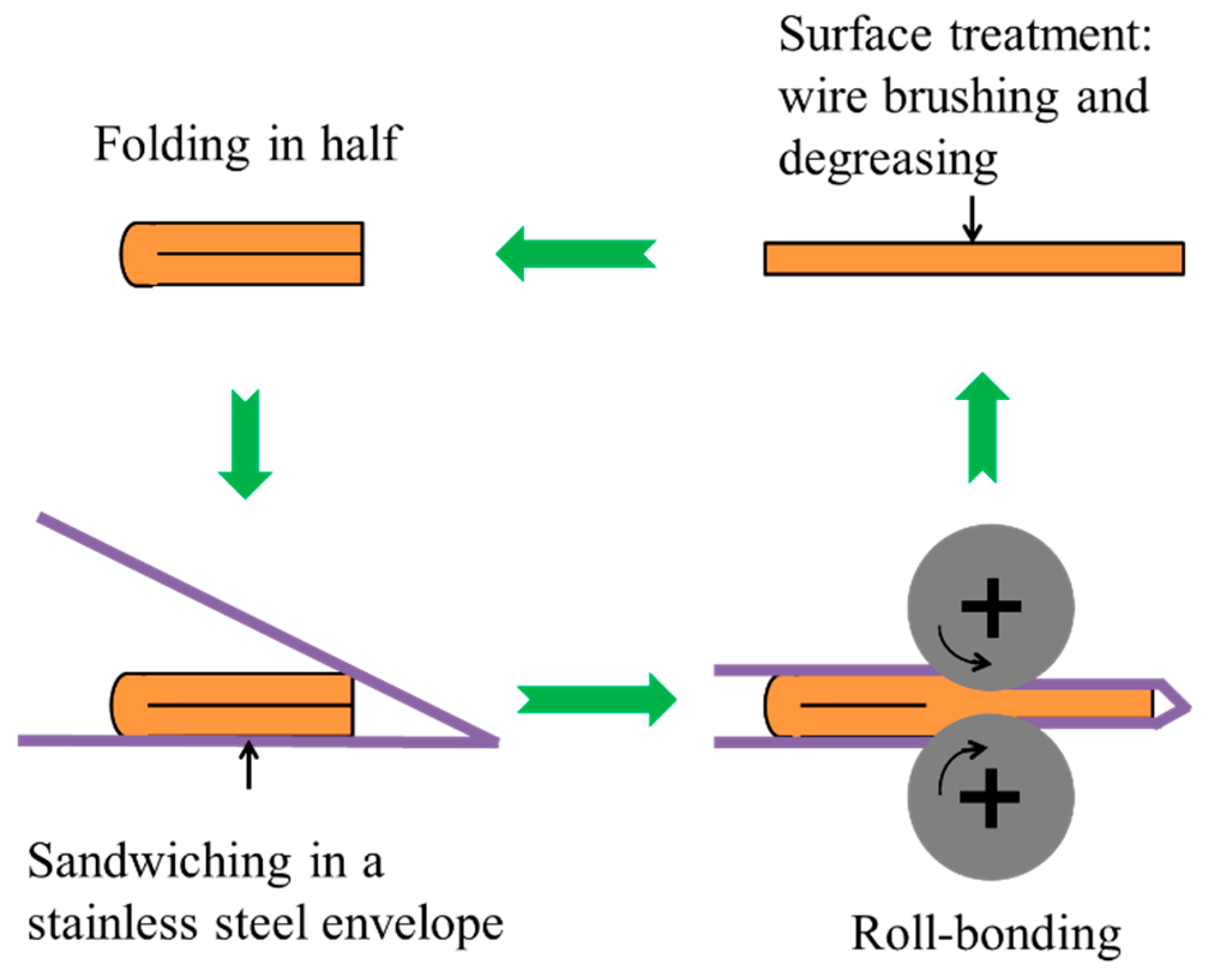
2. Experimental Procedure

Pure Cu (99.97%) sheets (Luoyang Copper Co., Ltd., Luoyang, China) with 1 mm in thickness were used in this study. As-received sheets were annealed in Ar atmosphere at 600 °C for 2 h before being cut into strips with dimensions of 200 mmL × 10 mmW × 1 mmT. The schematic of the modified ARB process is shown in Figure 1. As shown in Figure 1, the top surface of the Cu strip was wire-brushed and degreased by acetone. Unlike prior ARB procedures in literature, the Cu strip was folded in half by pliers instead of being cut in half, and then sandwiched in a stainless steel envelope. The envelope was made by folding a stainless steel plate with dimensions of 400 mmL × 100 mmW × 0.5 mmT in half and then rolling it with no thickness reduction. The sample in the envelope was then roll-bonded with a 50% reduction in thickness at room temperature without lubrication, at a rolling speed of 187 mm/min using a two-high rolling mill. The above procedures were repeated to the intended N and ARBed Cu samples with N = 1–30 were fabricated respectively. The equivalent strain imposed on samples was calculated as approximately 0.8 N [8].
To investigate the bonding condition of the ARBed samples, the rolling direction-normal direction (RD-ND) plane of each sample was observed. Microhardness of the samples was measured on the rolling direction-transverse direction (RD-TD) plane of each sample with a load of 100 gf and a duration of 10 s using a HXS-1000A microhardness tester (Shangguang Microscope Co., Ltd., Shanghai, China). Each data represents an average of ten randomly selected points. Electrical conductivity was measured on the RD-TD plane by an eddy-current electrical conductivity meter (FQR7501A, Xingsha Instrument Co., Ltd., Xiamen, China). Each piece of data represents an average of three measurements.

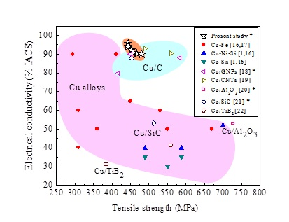
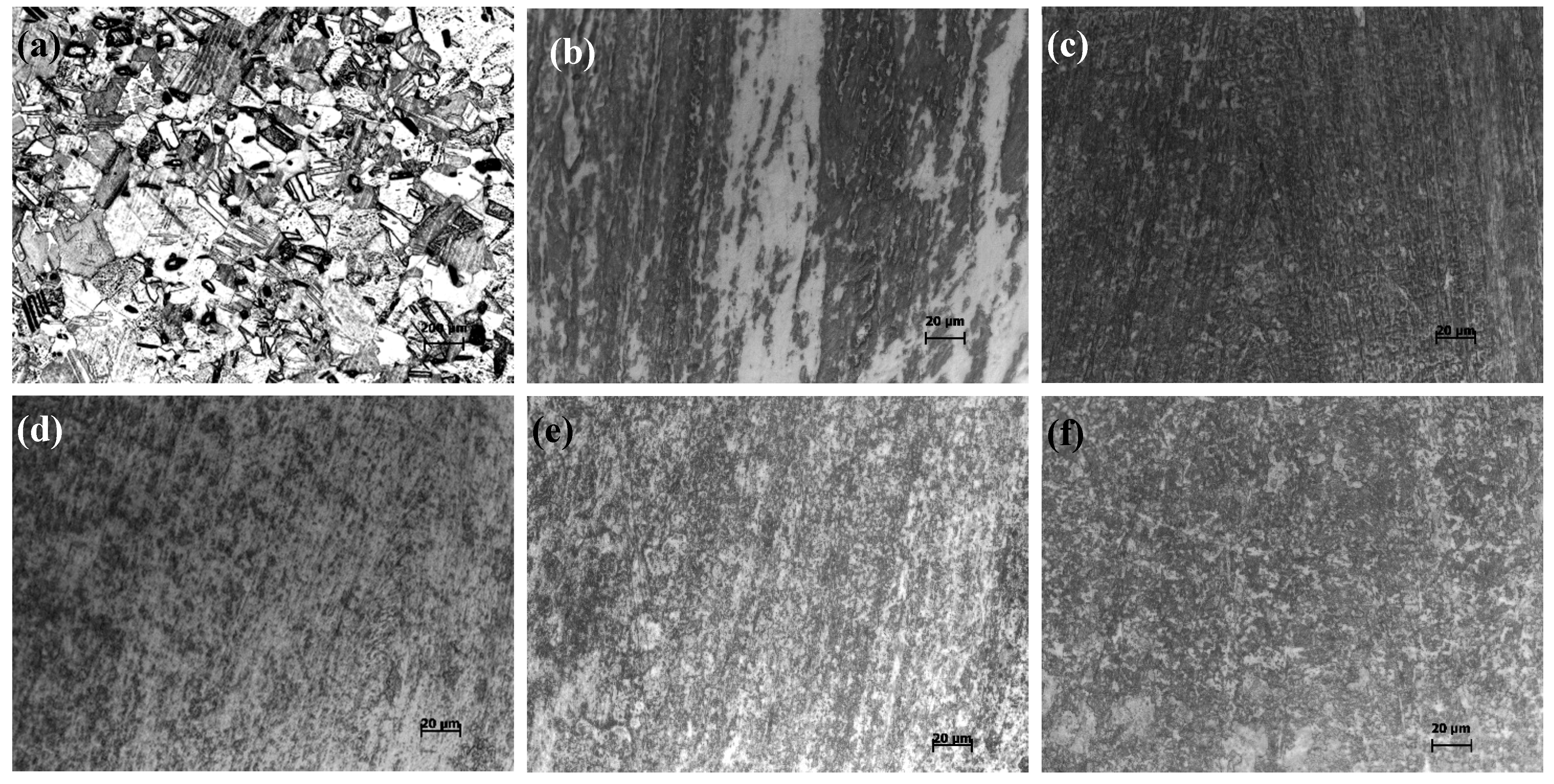
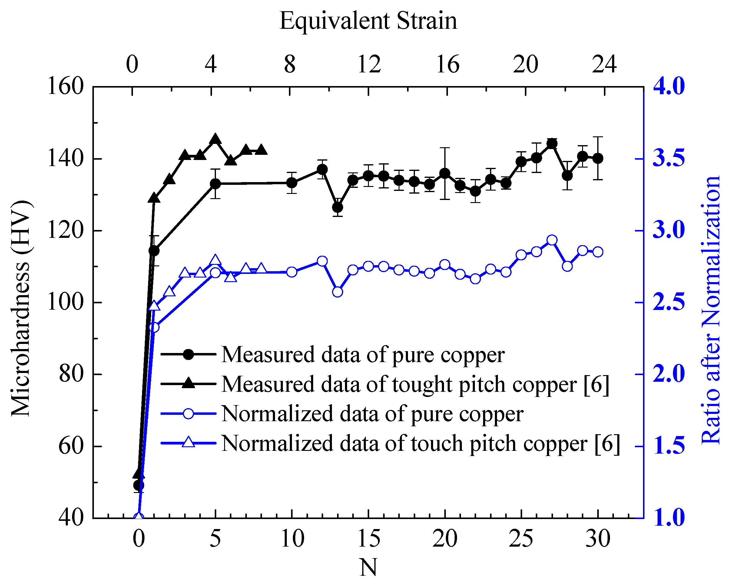
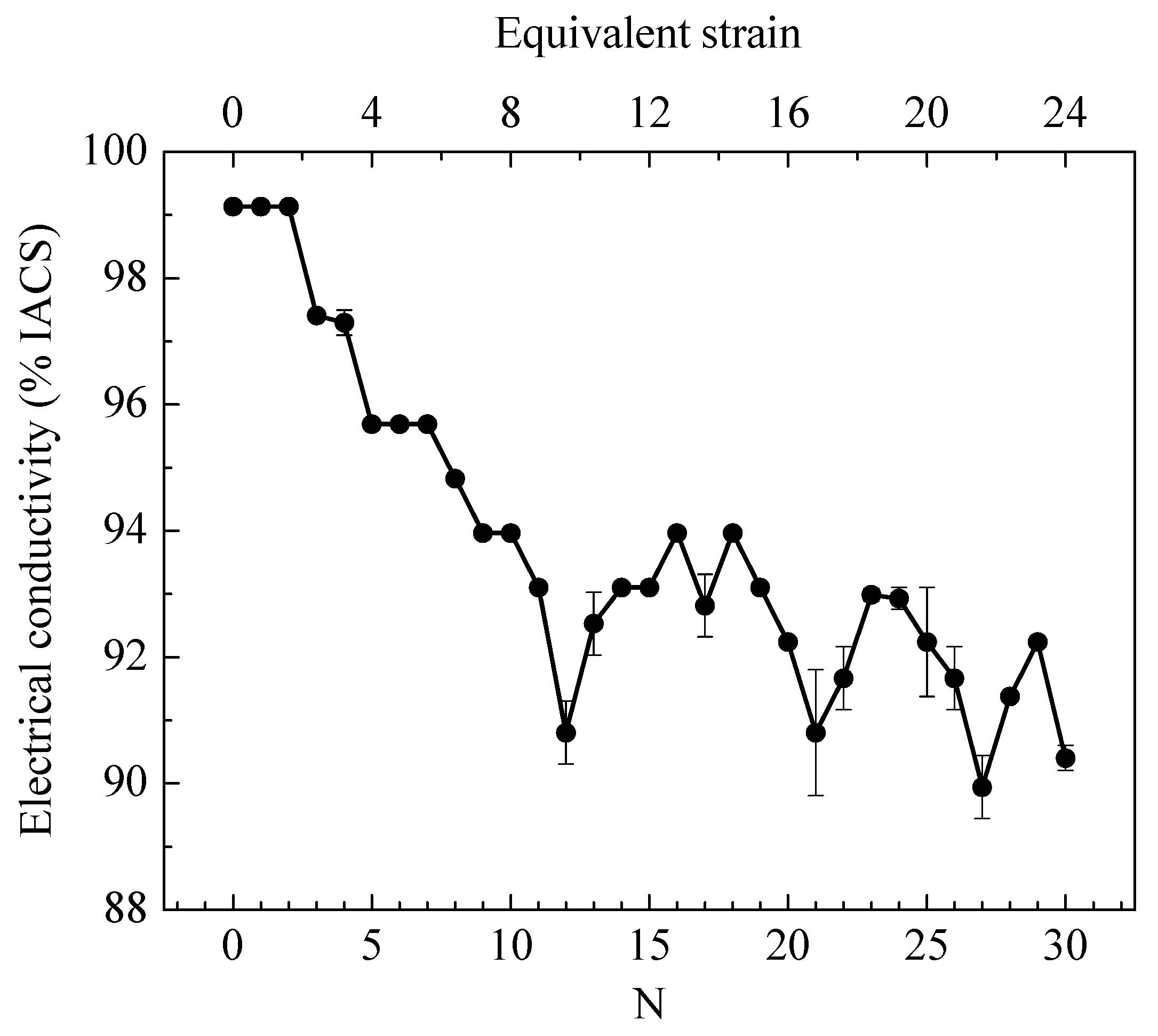
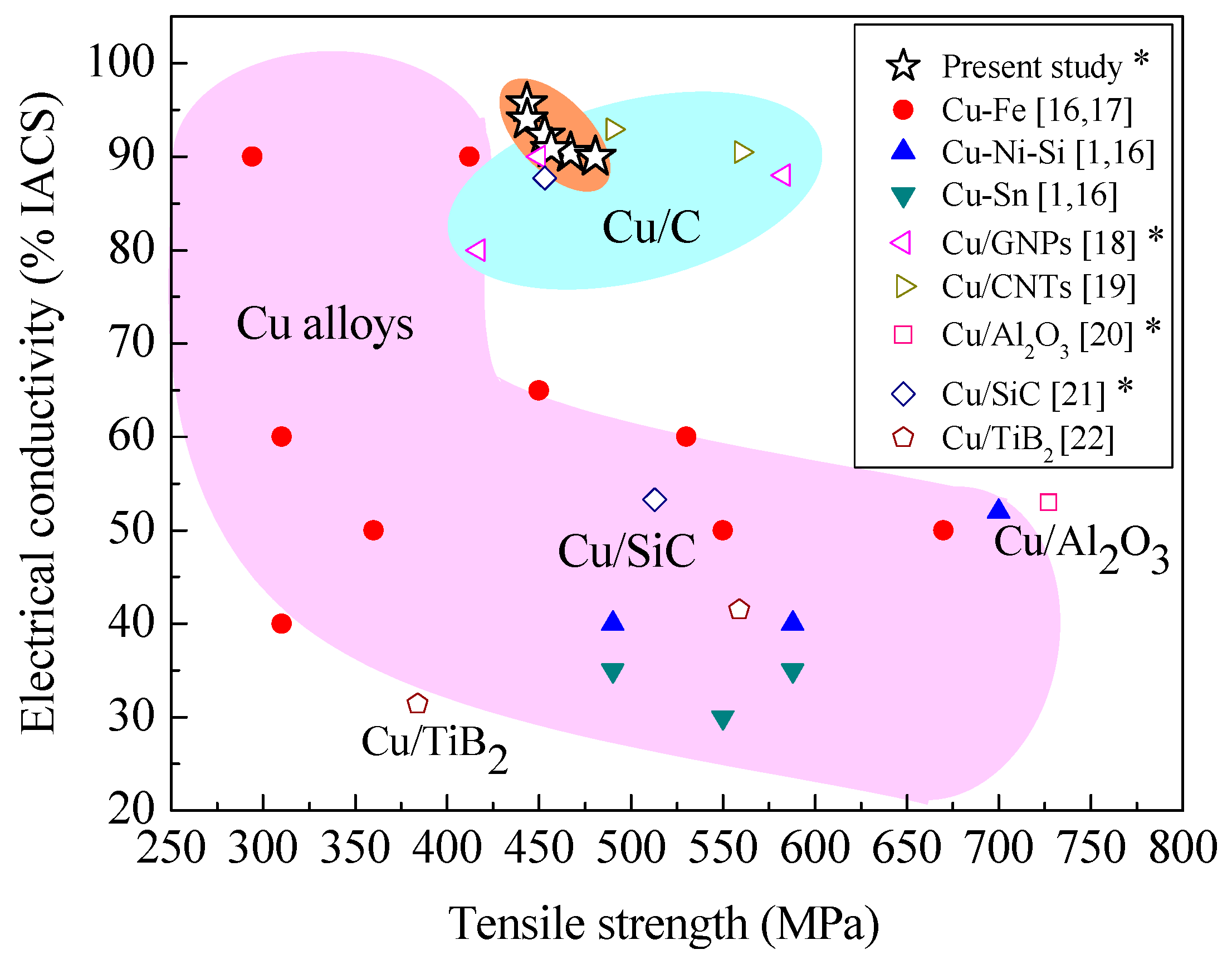
3. Results and Discussion

In the conventional ARB process, the roll-bonded sample is cut in half, stacked after surface treatment, and then rolled [5]. However, the independent upper layer and lower layer of the stacked sample can move freely during rolling, which will make the two layers diverge. The overlapping part and non-overlapping part of the two layers thus have different deformations, which facilitate the initiation and propagation of cracks in the sample, leading to the failure of the sample. To overcome this problem, fastening the four corners or two ends of the sample by wires was used in some studies [8,10]. The maximum cycle that can be performed was still limited as the large force during rolling could easily overcome the fastening. In this study, the Cu strip was folded as a whole for rolling. The folding end of the sample greatly limited the relative movement of the upper and lower layers of the sample during rolling. The stainless steel envelope further fixed the sample and homogenized the force during rolling. As a result, the crack of samples was inhibited and up to 30 cycles of ARB with a 50% thickness reduction per cycle (equivalent strain = 24) were successfully conducted on a copper sample at room temperature without intermediate annealing.
Microstructures of the RD-ND planes of samples with various N (N = 1, 5, 10, 20 and 30) and annealed Cu before ARB (N = 0) are shown in Figure 2. In contrast to the clear grain boundaries in Figure 2a, it is difficult to recognize the individual grains in Figure 2b–f as the grains have been severely deformed and significantly refined by ARB [5]. According to previous studies, the grains of ARBed Cu have been significantly refined, with an average grain size of ~260 nm–300 nm for N = 6–8 [5,11]. In this study, the optical micrographs are used to illustrate the bonding condition of ARBed samples on a relatively large scale, which is crucial for bulk structural materials. For ARBed samples, the theoretical number of interfaces between Cu layers is 2N − 1 (for N = 30, the theoretical number of interfaces is as large as 109). In Figure 2, no interfaces between the un-bonded layers can be seen, indicating the excellent bonding condition of the ARBed Cu samples.
The microhardness of the ARBed Cu as functions of both N and corresponding equivalent strain is shown in Figure 3. As shown in Figure 3, the microhardness of ARBed Cu increases with increasing N, but with a reduced rate accompanied by fluctuations from N = 5 to N = 30. Microhardness of the ARBed Cu sample with N = 30 is 140.1 HV, ~2.9 times that of initial annealed Cu. The evident increase of the microhardness of ARBed Cu mainly results from the strengthening effect due to accumulation of lattice defects and significant grain refinement at ultrahigh strains [6,12,13]. The reduced rate of the increase of microhardness of ARBed Cu with increasing strain can be attributed to the balance of the strengthening effect of strain hardening, fine grain boundary hardening and the softening effect of dynamic recovery [7,14,15].
Variation in microhardness of tough pitch copper (99.9%) processed by eight-cycle ARB reported by Shaarbaf et al. [6] is also shown in Figure 3 for comparison. The normalized hardness (ratio of the final microhardness to initial microhardness) of ARBed tough pitch copper with N = 8 is 2.7. The same ratio is obtained for ARBed Cu with N = 5 in the present study, and the ratio for ARBed Cu with N = 30 is 2.9. We found that the most evident increase in the microhardness of ARBed Cu occurred for N ≤ 5 in present study. Further deformation by ARB to N = 30 only brought slight increase in microhardness, which clearly indicates that the strengthening effect on pure copper induced by ARB has an upper limit. Meanwhile, the continuous increase of microhardness up to N = 30, although with much less evidently for N = 5–30, indicates the good bonding condition and intactness of the ARBed Cu samples with very high N since possible debonding and cracking in samples can induce significant decrease of hardness and electrical conductivity when N is very large.
Ductility is critical, especially for metals prepared by high-strain deformation. As for the ductility of ARBed Cu, Shaarbaf et al. [6] reported that the elongation of ARBed tough pitch copper (99.9%) decreases from ~50% to ~2% in the 1st cycle and then increases up to ~6% with N = 8. Jang et al. [11] reported a similar phenomenon that the elongation of ARBed Cu decreases greatly in the 1st cycle and then shows a gradual increase in following cycles, suggesting that the strain hardening alone can not explain this phenomenon. The effect of ultrahigh strains on the ductility of ARBed Cu is two-fold, i.e., it can induce loss in ductility due to strain hardening and induce increase in ductility due to dynamic recovery. However, further study is needed to clarify this point. On the other hand, for applicants that require a combination of high microhardness and electrical conductivity, e.g., lead frames and welding electrodes, the ductility may not be a main requirement. For example, the elongations of C19400, NK-120 and C70250 used for lead frames are 4%–5%, 5% and 2%–6% respectively [1,16]. Thus, the ARBed Cu in the present study can be a potential candidate for these applications despite the reduced ductility.
Figure 4 illustrates the electrical conductivity (σ) of the ARBed Cu versus N as well as corresponding equivalent strain. As shown in Figure 4 σ decreases only slightly with increasing N. For N = 30, σ of the ARBed Cu is still 90.4% IACS, only 8.7% IACS smaller than initial annealed Cu (N = 0). Most interestingly, we observed evident periodic fluctuations in the σ of ARBed Cu for N > 10. Such fluctuations are believed to be associated with alternating accumulation and annihilation of lattice defects. When Cu is deformed by ARB to high strains, accumulation of lattice defects (e.g., dislocations) can induce a decrease in the electrical conductivity. Meanwhile, dynamic recovery can induce an increase in the electrical conductivity due to annihilation of defects. Usually, dynamic recovery is driven by the increase of strain energy to a critical level. After dynamic recovery, the strain energy in the sample is released and then further accumulation of lattice defects is possible. This may lead to the alternating decrease and increase of lattice defects during the deformation of the sample, which will induce the alternating decrease and increase of the electrical conductivity. Nevertheless, further study, e.g., a direct characterization of the lattice defects is needed to clarify this point.
The above results show that the ARBed Cu has a good combination of hardness and electrical conductivity. Figure 5 presents the electrical conductivity-strength relationships of the ARBed Cu samples in the present study (N = 5, 10, 12, 20, 27, 30), and high-strength, high-conductivity Cu alloys [1,16,17] used for lead frames and Cu based composites (including Cu/GNPs (graphene nanoplatelets) [18], Cu/CNTs (carbon nanotubes) [19], Cu/Al2O3 [20], Cu/SiC [21], Cu/TiB2 [22]) are also included for comparison. The strength of the ARBed Cu, Cu/GNPs, Cu/Al2O3 and Cu/SiC was calculated as H/3 [23,24], where H is the microhardness of the material. As shown in Figure 5, the ARBed Cu samples have a better combination of strength and electrical conductivity than most high-strength, high-conductivity Cu alloys, Cu/Al2O3, Cu/SiC, Cu/TiB2, and are similar to Cu/C composites (including Cu/GNPs and Cu/CNTs). Obviously, our results indicate the effectiveness of ARB for producing high-strength and high-electrical-conductivity Cu.

4. Conclusions

By modifying the ARB procedures, we successfully conducted ARB processing up to 30 cycles with a 50% thickness reduction per cycle (equivalent strain = 24) at room temperature on pure copper. We found that good bonding condition was achieved for the ARBed samples. The microhardness of ARBed Cu samples increases rapidly at first and then is almost saturated from the 5th cycle to the 30th cycle, ~2.9 times that of the annealed pure copper for N = 30. The electrical conductivity decreases with increasing N, all larger than 90% IACS for various N. The variations of microhardness and electrical conductivity with ARB strains can be understood considering the strengthening effects due to accumulation of lattice defects and significant grain refinement and the softening effect due to dynamic recovery. The ARBed Cu has a better combination of strength and electrical conductivity than common Cu alloys, and is even comparable to Cu matrix composites reinforced by GNPs or CNTs. Our study indicates the effectiveness of ARB processing for fabrication of high-strength and high-conductivity pure copper.

Acknowledgements

This work was financially supported by the National Natural Science Foundation of China (grant 51371128) and the research foundation of Wuhan University.

Author Contributions

Q.S.M. and J.L. conceived and designed the experiments; G.Y., C.L., Y.M. and F.C. performed the experiments; G.Y. and Q.S.M. analyzed the data; G.Z. and B.Y. contributed analysis tools and discussion of results; G.Y. and Q.S.M. wrote the paper.

Conflicts of Interest

The authors declare no conflicts of interest.

References

  1. Tomioka, Y.; Miyake, J. A copper alloy development for leadframe. In Proceedings of 1995 Electronic Manufacturing Technology Symposium, Omiya, Japan, 4–6 December 1995; pp. 433–436.
  2. Suzuki, S.; Shibutani, N.; Mimura, K.; Isshiki, M.; Waseda, Y. Improvement in strength and electrical conductivity of Cu–Ni–Si alloys by aging and cold rolling. J. Alloy. Compd. 2006, 417, 116–120. [Google Scholar] [CrossRef]
  3. Lu, D.P.; Wang, J.; Zeng, W.J.; Liu, Y.; Lu, L.; Sun, B.D. Study on high-strength and high-conductivity Cu-Fe-P alloys. Mater. Sci. Eng. A 2006, 421, 254–259. [Google Scholar] [CrossRef]
  4. Ghosh, G.; Miyake, J.; Fine, M.E. The systems-based design of high-strength, high-conductivity alloys. JOM 1997, 49, 56–60. [Google Scholar] [CrossRef]
  5. Tsuji, N.; Saito, Y.; Lee, S.H.; Minamino, Y. ARB (Accumulative Roll-Bonding) and other new Techniques to Produce Bulk Ultrafine Grained Materials. Adv. Eng. Mater. 2003, 5, 338–344. [Google Scholar] [CrossRef]
  6. Shaarbaf, M.; Toroghinejad, M.R. Nano-grained copper strip produced by accumulative roll bonding process. Mater. Sci. Eng. A 2008, 473, 28–33. [Google Scholar] [CrossRef]
  7. Jang, Y.; Kim, S.; Han, S.; Lim, C.; Goto, M. Tensile behavior of commercially pure copper sheet fabricated by 2- and 3-layered accumulative roll bonding (ARB) process. Met. Mater. Int. 2008, 14, 171–175. [Google Scholar] [CrossRef]
  8. Saito, Y.; Utsunomiya, H.; Tsuji, N.; Sakai, T. Novel ultra-high straining process for bulk materials—Development of the accumulative roll-bonding (ARB) process. Acta Mater. 1999, 47, 579–583. [Google Scholar] [CrossRef]
  9. Kunimine, T.; Fujii, T.; Onaka, S.; Tsuji, N.; Kato, M. Effects of Si addition on mechanical properties of copper severely deformed by accumulative roll-bonding. J. Mater. Sci. 2011, 46, 4290–4295. [Google Scholar] [CrossRef]
  10. Suresh, K.S.; Sinha, S.; Chaudhary, A.; Suwas, S. Development of microstructure and texture in Copper during warm accumulative roll bonding. Mater. Charact. 2012, 70, 74–82. [Google Scholar] [CrossRef]
  11. Jang, Y.H.; Kim, S.S.; Han, S.Z.; Lim, C.Y.; Kim, C.J.; Goto, M. Effect of trace phosphorous on tensile behavior of accumulative roll bonded oxygen-free copper. Scr. Mater. 2005, 52, 21–24. [Google Scholar] [CrossRef]
  12. Jamaati, R.; Toroghinejad, M.R. Application of ARB process for manufacturing high-strength, finely dispersed and highly uniform Cu/Al2O3 composite. Mater. Sci. Eng. A 2010, 527, 7430–7435. [Google Scholar] [CrossRef]
  13. Xing, Z.P.; Kang, S.B.; Kim, H.W. Structure and properties of AA3003 alloy produced by accumulative roll bonding process. J. Mater. Sci. 2002, 37, 717–722. [Google Scholar] [CrossRef]
  14. Eizadjou, M.; Manesh, H.D.; Janghorban, K. Microstructure and mechanical properties of ultra-fine grains (UFGs) aluminum strips produced by ARB process. J. Alloy. Compd. 2009, 474, 406–415. [Google Scholar] [CrossRef]
  15. Shih, M.H.; Yu, C.Y.; Kao, P.W.; Chang, C.P. Microstructure and flow stress of copper deformed to large plastic strains. Scr. Mater. 2001, 45, 793–799. [Google Scholar] [CrossRef]
  16. Ma, J.S.; Huang, F.X.; Huang, L.; Geng, Z.T.; Ning, H.L.; Han, Z.Y. Trends and development of copper alloys for lead frame. J. Funct. Mater. 2002, 33, 1–4. [Google Scholar]
  17. ASM handbook committee. Metals Handbook Volume 2, 9th ed.; ASM: Metals Park, OH, USA, 1979; pp. 310–313. [Google Scholar]
  18. Chen, F.; Ying, J.; Wang, Y.; Du, S.; Liu, Z.; Huang, Q. Effects of graphene content on the microstructure and properties of copper matrix composites. Carbon 2016, 96, 836–842. [Google Scholar] [CrossRef]
  19. Arnaud, C.; Lecouturier, F.; Mesguich, D.; Ferreira, N.; Chevallier, G.; Estournès, C.; Weibel, A.; Laurent, C. High strength–High conductivity double-walled carbon nanotube–Copper composite wires. Carbon 2016, 96, 212–215. [Google Scholar] [CrossRef]
  20. Rajkovic, V.; Bozic, D.; Stasic, J.; Wang, H.; Jovanovic, M.T. Processing, characterization and properties of copper-based composites strengthened by low amount of alumina particles. Powder Technol. 2014, 268, 392–400. [Google Scholar] [CrossRef]
  21. Efe, G.C.; Yener, T.; Altinsoy, I.; Ipek, M.; Zeytin, S.; Bindal, C. The effect of sintering temperature on some properties of Cu-SiC composite. J. Alloy. Compd. 2011, 509, 6036–6042. [Google Scholar]
  22. López, M.; Corredor, D.; Camurri, C.; Vergara, V.; Jiménez, J. Performance and characterization of dispersion strengthened Cu-TiB2 composite for electrical use. Mater. Charact. 2005, 55, 252–262. [Google Scholar] [CrossRef]
  23. Zhang, P.; Li, S.X.; Zhang, Z.F. General relationship between strength and hardness. Mater. Sci. Eng. A 2011, 529, 62–73. [Google Scholar] [CrossRef]
  24. Cahoon, J.R.; Broughton, W.H.; Kutzak, A.R. The determination of yield strength from hardness measurements. Metall. Trans. 1971, 2, 1979–1983. [Google Scholar]
Figure 1. Schematic of the modified ARB process.
Metals 06 00115 g001
Figure 2. Micrographs of (a) annealed Cu before ARB, RD-ND planes of ARBed Cu samples with N = (b) 1, (c) 5, (d) 10, (e) 20 and (f) 30.
Metals 06 00115 g002
Figure 3. Microhardness of ARBed Cu in the present study and ARBed tough pitch copper [6] as functions of N and corresponding equivalent strain, before and after normalization.
Metals 06 00115 g003
Figure 4. Electrical conductivity of ARBed Cu versus N and equivalent strain.
Metals 06 00115 g004
Figure 5. Electrical conductivity versus tensile strength of ARBed Cu (N = 5, 10, 12, 20, 27, 30) in this study, high-strength, high-conductivity Cu alloys [1,16,17] and common Cu based composites [18,19,20,21,22]. * tensile strength is calculated as H/3 [23,24].
Metals 06 00115 g005

