
Picosecond Laser Shock Peening of Nimonic 263 at 1064 nm and 532 nm Wavelength

Abstract
:
1. Introduction
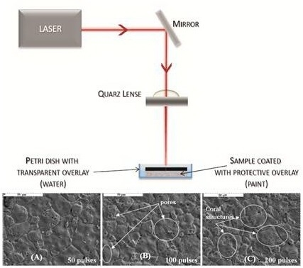
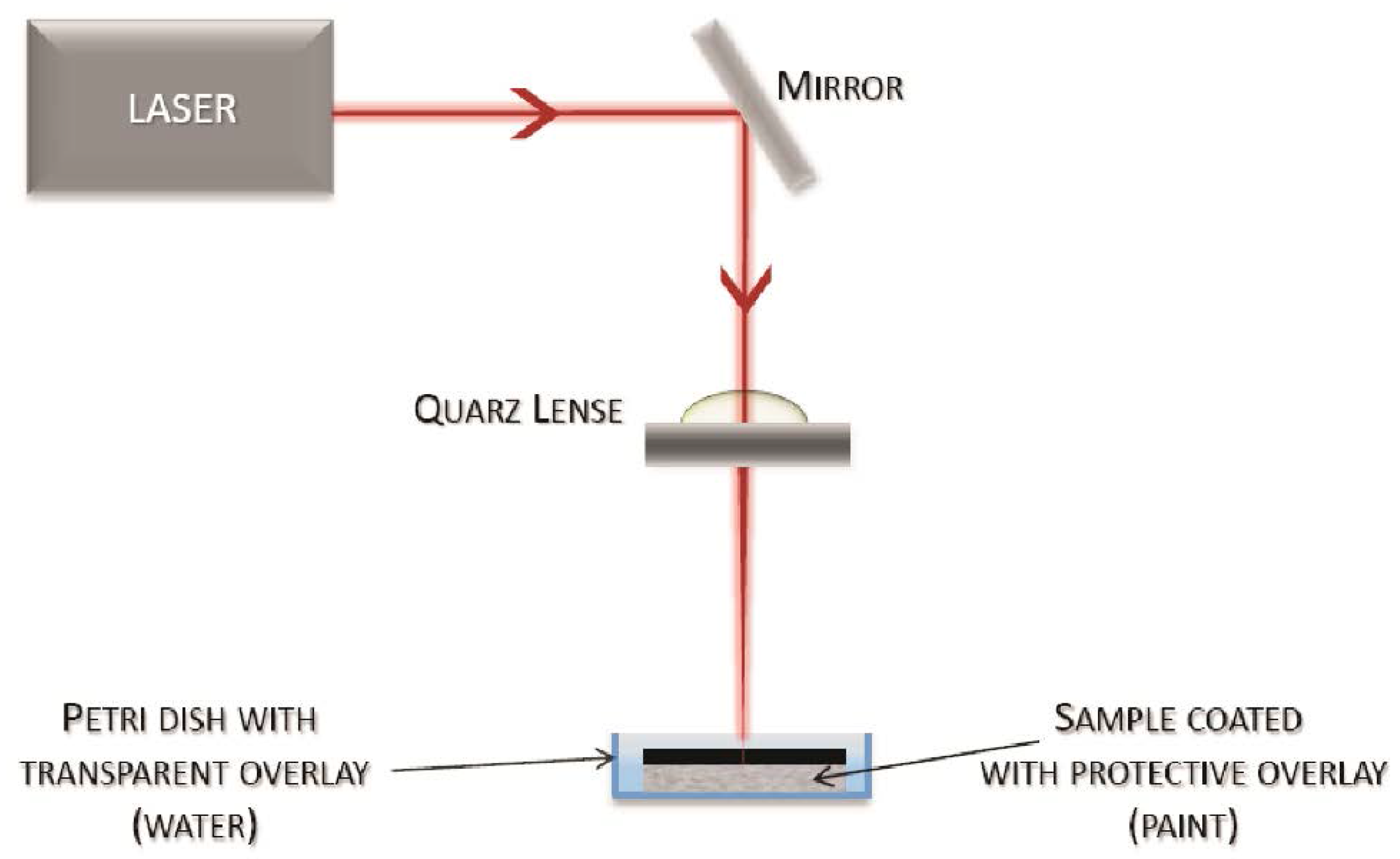
2. Experimental Section
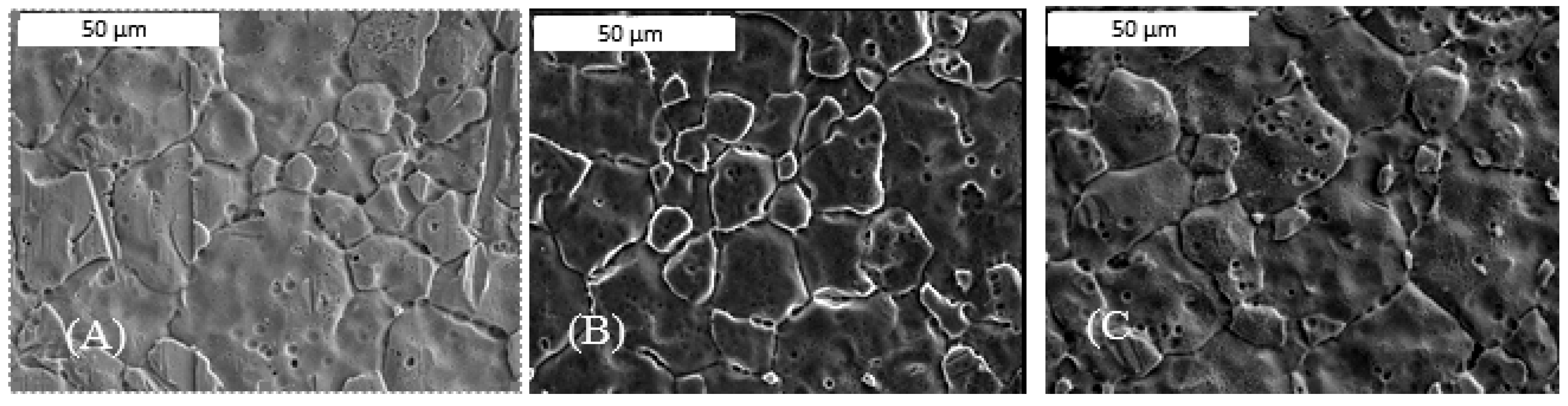
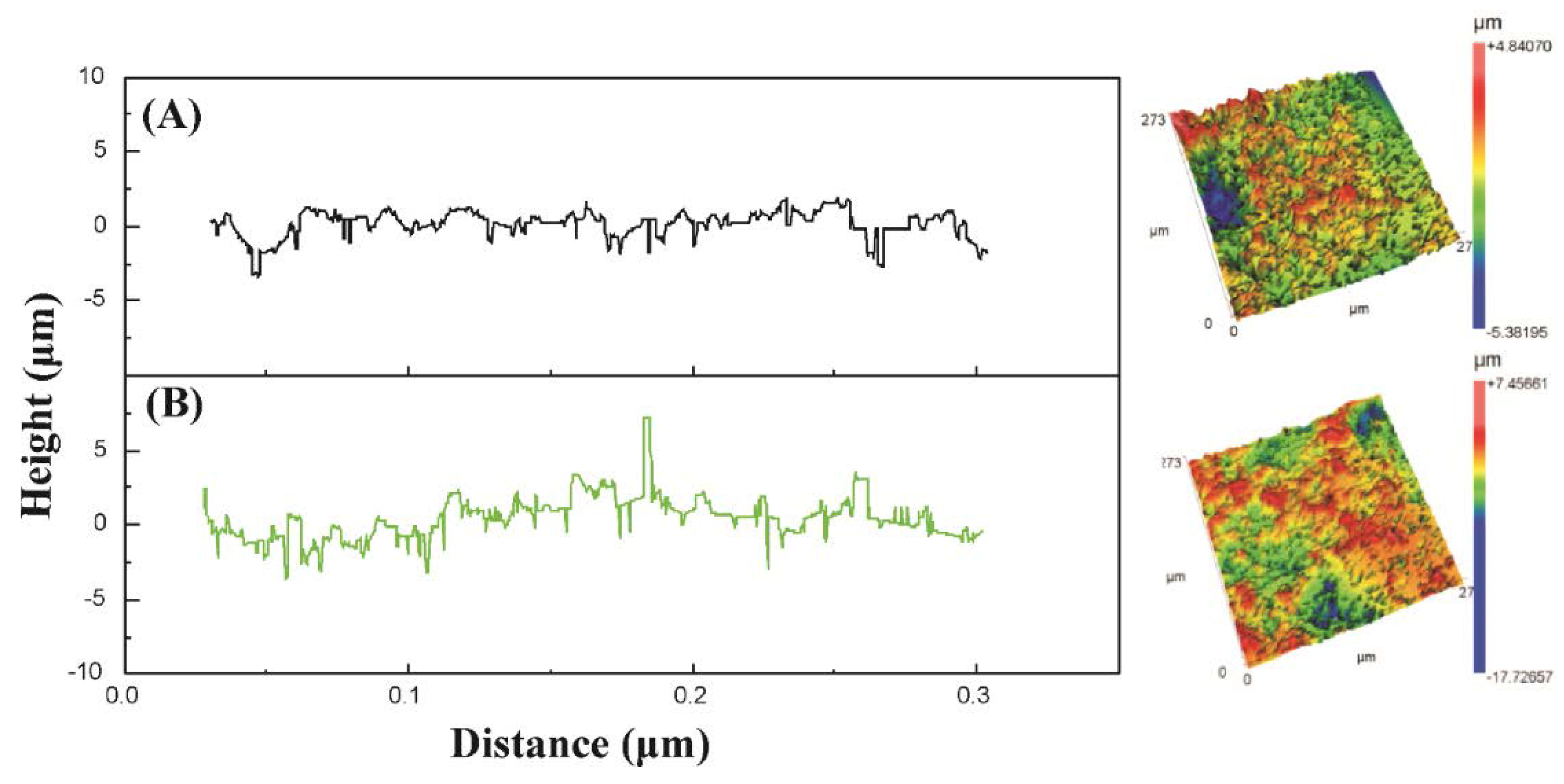
3. Results and Discussion
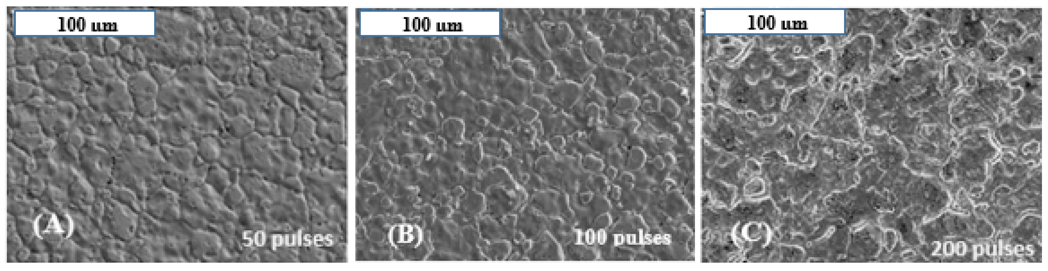
3.1. Laser Shock Peening of Nimonic 263 at 1064 nm Wavelength
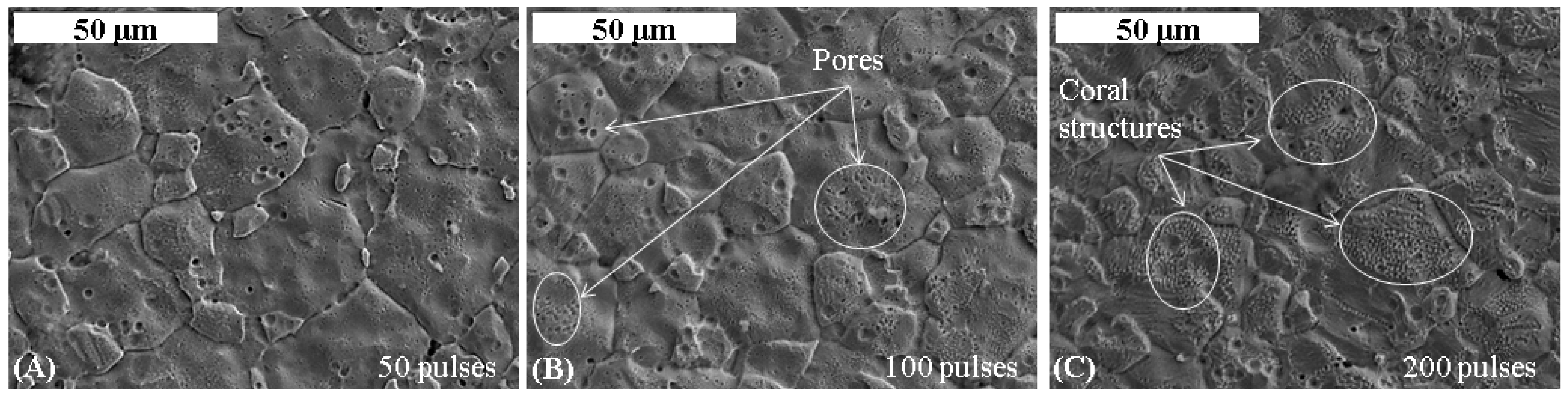
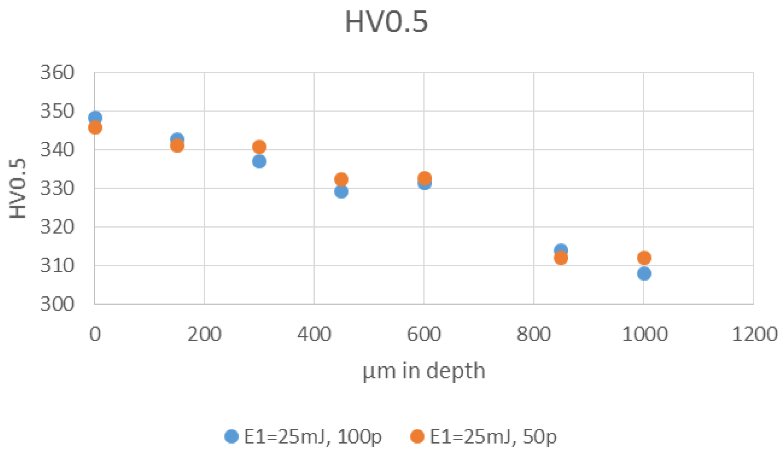
3.2. Laser Shock Peening of Nimonic 263 at 532 nm Wavelength
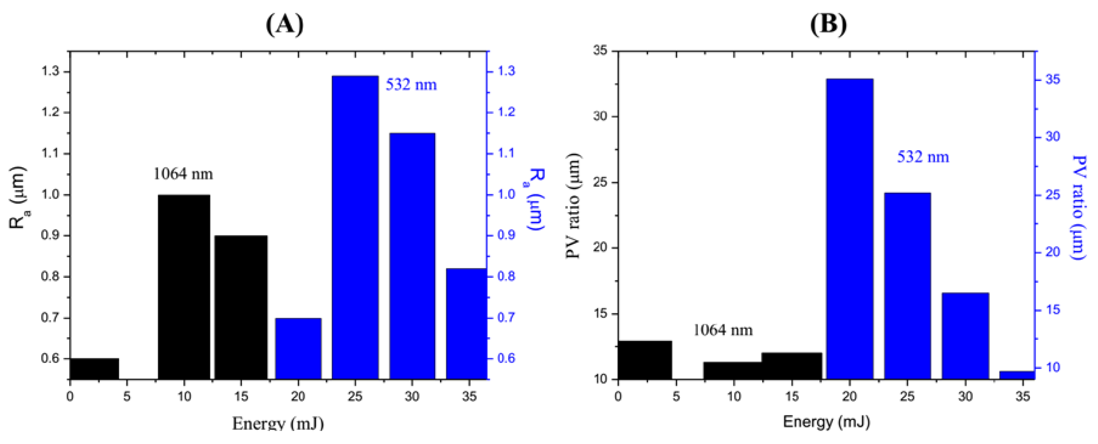
3.3. Comparison of Results Obtained by Laser Operating at 1064 nm and 532 nm
4. Conclusions
Acknowledgments
Author Contributions
Conflicts of Interest
References
- Pollock, M.T.; Tin, S. Nickel-Based Superalloys for Advanced Turbine Engines: Chemistry, Microstructure, and Properties. J. Propuls. Power 2006, 22, 361–374. [Google Scholar] [CrossRef]
- Shahriari, D.; Sadeghi, M.H.; Akbarzadeh, A.; Cheraghzade, M. The influence of heat treatment and hot deformation conditions on γ′ precipitate dissolution of Nimonic 115 superalloy. J. Adv. Manuf. Technol. 2009, 45, 841–850. [Google Scholar] [CrossRef]
- Singh, P.N.; Singh, V. Influence of ageing treatment on work hardening behavior of Ni-base superalloy. Scr. Mater. 1996, 34, 1861–1865. [Google Scholar] [CrossRef]
- Park, N.K.; Kim, I.S.; Na, Y.S.; Yeom, J.T. Hot forging of a nickel-base superalloy. J Mater. Process. Technol. 2001, 111, 98–102. [Google Scholar] [CrossRef]
- Milovanovic, D.S.; Radak, B.B.; Gakovic, B.M.; Batani, D.; Momcilovic, M.D.; Trtica, M.S. Surface morphology modifications of titanium based implant induced by 40 picosecond laser pulses at 266 nm. J. Alloy Compd. 2010, 501, 89–92. [Google Scholar] [CrossRef]
- Petronic, S.; Milovanovic, D.; Milosavljevic, A.; Momcilovic, M.; Petrusko, D. Influence of picosecond laser irradiation on nickel-based superalloy surface microstructure. Phys Scr. 2012. [Google Scholar] [CrossRef]
- Yilbas, B.S.; Shuja, S.Z.; Arif, A.; Gondal, M.A. Laser-shock processing of steel. J. Mater. Proc. Technol. 2003, 135, 6–17. [Google Scholar] [CrossRef]
- Peyre, P.; Fabbro, R. Laser shock processing: A review of the physics and applications. Opt. Quantum Electr. 1995, 27, 1213–1229. [Google Scholar]
- Devaux, D.; Fabbro, R.; Tollier, L.; Bartnicki, E. Generation of shock waves by laser-induced plasma in confined geometry. J. Appl. Phys. 1993, 74, 2268–2273. [Google Scholar] [CrossRef]
- Peyre, P.; Fabbro, R.; Berthe, L.; Dubouchet, C. Laser shock processing of materials, physical processes involved and examples of application. J. Laser Appl. 1996, 8, 135–141. [Google Scholar] [CrossRef]
- Zhong, H.; Yu, C. Laser shock processing of 2024-T62 aluminum alloy. Mater. Sci. Eng. A 1998, 257, 322–327. [Google Scholar]
- Clauer, A.H.; Holbrook, J.H.; Fairand, B.P. Effects of laser induced shock waves. In Shock Waves and High-Strain, Phenomena in Metals; Meyers, M.A., Murr, L.E., Eds.; Plenum Press: New York, NY, USA, 1981; pp. 675–703. [Google Scholar]
- Amarchinta, H.K.; Grandhi, R.V.; Clauer, A.H.; Langer, K.; Stargel, D.S. Simulation of residual stress induced by a laser peening process through inverse optimization of material models. J. Mater. Process. Technol. 2010, 210, 1997–2006. [Google Scholar] [CrossRef]
- Peyre, P.; Chaieb, I.; Braham, C. FEM calculation of residual stresses induced by laser shock processing in stainless steels. Model. Simul. Mater. Sci. Eng. 2007, 15, 205–221. [Google Scholar] [CrossRef]
- Sibalija, T.; Petronic, S.; Majstorovic, V.; Milosavljevic, A. Modelling and optimisation of laser shock peening using an integrated simulated annealing-based method. Int. J. Adv. Manuf. Technol. 2014, 73, 1141–1158. [Google Scholar] [CrossRef]
- Ding, K.; Ye, L. Laser Shock Peening, Performance and Process Simulation; Woodhead Publishing Limited: Cambridge, UK, 2006; pp. 50–53. [Google Scholar]
- Schijve, J. Fatigue of Structures and Materials; Kluwer Academic Publisher: Dordrecth, The Netherlands, 2001; pp. 71–78. [Google Scholar]
- Lee, D. Feasibility Study on Laser Microwelding and Laser Shock Peening Using Femtosecond Laser Pulses. Ph.D. Thesis, University of Michigen, Ann Arbor, MI, USA, 2008. [Google Scholar]
- Semaltianos, N.G.; Perrie, W.; French, P.; Sharp, M.; Dearden, G.; Logothetidis, S.; Watkins, K.G. Femtosecond laser ablation characteristics of nickel-based superalloy C263. Appl. Phys. A 2009, 94, 999–1009. [Google Scholar] [CrossRef]
- Gomez-Rosas, G.; Rubio-Gonzalez, C.; Ocaña, J.L.; Molpeceres, C.; Porro, J.A.; Morales, M.; Casillas, F.J. Laser Shock Processing of 6061-T6 Al alloy with 1064 nm and 532 nm wavelengths. Appl. Surf. Sci. 2010, 256, 5828–5831. [Google Scholar] [CrossRef]
- Schumann, H. Metallographie; Deutscher Verlag fuer Grundstoffindustrie: Leipzig, Germany, 1974; p. 15. [Google Scholar]
- Petronic, S.; Burzic, M.; Milovanovic, D.; Colic, K.; Radovanovic, Z. Picosecond laser shock peening of base material Nimonic 263 material and laser welded Nimonic 263 alloy. Weld. Weld. Struct. 2015, 60, 149–155. [Google Scholar]
- Petronic, S.; Kovacevic, A.G.; Milosavljevic, A.; Sedmak, A. Microstructural changes of Nimonic 263 superalloy caused by laser beam action. Phys. Scr. 2012. [Google Scholar] [CrossRef]
- Bauerle, D. Laser Processing and Chemistry; Springer Verlag: Berlin, Germany, 2003; pp. 13–256. [Google Scholar]
- Peyre, P.; Berthe, L.; Scherpereel, X.; Fabbro, R.; Bartniki, E. Experimental Study of Laser-Driven Shock Waves in Stainless Steels. J. Appl. Phys. 1998, 84, 5985–5992. [Google Scholar] [CrossRef]
- Niehofff, H.S.; Vollertsen, F. Laser induced shock waves in deformation processing. J. Metall. 2005, 11, 183–194. [Google Scholar]
- Berthe, L.; Fabbro, R.; Peyre, P.; Tollier, L.; Bartnicki, E. Shock waves from a water-confined laser-generated plasma. J. Appl. Phys. 1997, 82, 2826–2832. [Google Scholar] [CrossRef]
- Drobnjak. Physical metallurgy; Faculty of Technology and Metallurgy, University of Belgrade: Belgrade, Serbia, 1981; pp. 75–77. [Google Scholar]
- Matijasevic, B.; Kinder, J.; Radovic, N.A.; Volkov-Husovic, T. Shot-peening induced twinning in ship-building steel. Metalurgija 2002, 8, 149–155. [Google Scholar]
- Zhang, Y.K.; Lu, J.Z.; Ren, X.D.; Yao, H.B.; Yao, H.X. Effect of laser shock processing on the mechanical properties and fatigue lives of the turbojet engine blades manufactured by LY2 aluminum alloy. Mater. Des. 2009, 30, 1697–1703. [Google Scholar] [CrossRef]
- Schneider, M.S.; Kad, B.; Kalantar, D.H.; Remington, B.A.; Kenik, E.; Jarmakani, H.; Meyers, M.A. Laser shock compression of copper and copper-aluminum alloys. Int. J. Impact Eng. 2005, 32, 473–507. [Google Scholar] [CrossRef]
- Reed, R. The Superalloys—Fundamentals and Applications; Cambridge University Press: New York, NY, USA, 2006. [Google Scholar]
- Chena, C.Y.; Yena, H.W.; Kaoa, F.H.; Li, W.C.; Huang, C.Y.; Yanga, J.R.; Wang, S.H. Precipitation hardening of high-strength low-alloy steels by nanometer-sized carbides. Mater. Sci. Eng. A 2009, 499, 162–166. [Google Scholar] [CrossRef]
- Jang, J.H.; Lee, C.H.; Heo, Y.U.; Suh, D.H. Stability of (Ti, M)C (M = Nb, V, Mo and W) Carbide in Steels using First-Principles Calculations. Acta Mater. 2012, 60, 208–217. [Google Scholar] [CrossRef]
- Ren, X.D.; Zhang, Y.K.; Zhang, T.; Jiang, D.W.; Yongzhuo, H.F.; Jiang, Y.F.; Chen, K.M. Comparison of the simulation and experimental fatigue crack behaviours in the nanoseconds laser shocked aluminum alloy. Mater. Des. 2011, 32, 1138–1143. [Google Scholar] [CrossRef]
- Warren, A.W.; Guo, Y.B.; Chen, S.C. Massive parallel laser shock peening: Simulation, analysis, and validation. Int. J. Fatigue 2008, 30, 188–197. [Google Scholar] [CrossRef]
- Fabbro, R.; Fournier, J.; Ballard, P.; Devaux, D.; Virmont, J. Physical study of laser-produced plasma in confined geometry. J. Appl. Phys. 1990. [Google Scholar] [CrossRef]
- Grinspan, A.S.; Gnanamoorthy, R. Surface modification by oil jet peening in Al alloys, AA6063-T6 and AA6061-T4 Part 2: Surface morphology, erosion, and mass loss. Appl. Surf. Sci. 2006, 253, 997–1005. [Google Scholar] [CrossRef]


| Element | C | Si | Mn | Al | Co | Cr | Cu | Fe | Mo | Ti | Ni |
|---|---|---|---|---|---|---|---|---|---|---|---|
| % | 0.06 | 0.3 | 0.5 | 0.5 | 20 | 20 | 0.1 | 0.5 | 5.9 | 2.2 | 49.94 |
| Laser | Nd:YAG |
|---|---|
| Wavelenght | 532 nm, 1064 nm |
| Pulse duration | 150 ps |
| Mode | about TEM00 |
| Repetition rate | 10 Hz |
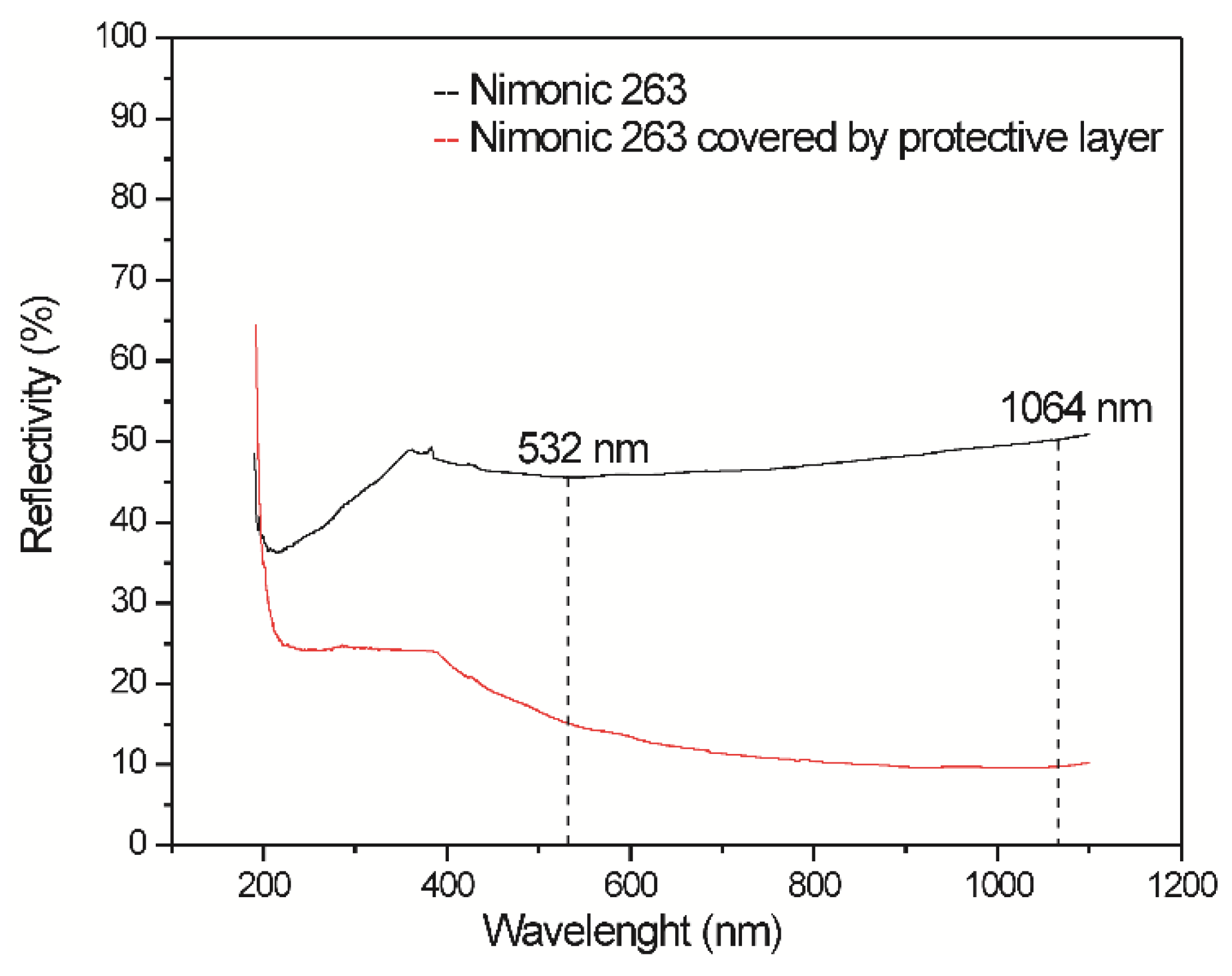
| Wavelength (nm) | Reflectivity (%) | |
|---|---|---|
| Nimonic 263 | Nimonic 263 with protective layer | |
| 532 | 45.6 | 15.0 |
| 1064 | 50.2 | 9.8 |
| Spectrum | C | Al | Si | Ti | Cr | Mn | Fe | Co | Ni | Mo |
|---|---|---|---|---|---|---|---|---|---|---|
| Spectrum 1 | 11.79 | 0.11 | 0.15 | 49.87 | 6.96 | 0.20 | 0.19 | 7.41 | 18.79 | 4.52 |
| Spectrum 2 | 14.56 | 0.13 | 0.19 | 13.36 | 11.56 | 1.00 | 0.33 | 13.22 | 34.04 | 12.19 |
| Spectrum 3 | 12.84 | 0.25 | 0.20 | 4.67 | 14.25 | 0.54 | 0.30 | 16.82 | 44.75 | 5.38 |
| Spectrum 4 | 18.29 | 1.02 | 0.94 | 21.59 | 9.62 | 0.35 | 0.24 | 10.67 | 27.73 | 9.54 |
| Spectrum | C | O | Al | Si | Ti | Cr | Mn | Fe | Co | Ni | Mo |
|---|---|---|---|---|---|---|---|---|---|---|---|
| Figure 7a | 11.49 | 6.92 | 0.28 | 0.23 | 1.58 | 15.59 | 0.45 | 0.43 | 16.69 | 41.79 | 4.57 |
| Spectrum 1 | 13.25 | - | 0.13 | 0.2 | 25.94 | 9.66 | 0.34 | 0.24 | 8.82 | 21.98 | 19.45 |
| Spectrum 2 | 12.96 | - | 0.18 | 0.25 | 20.15 | 11.50 | 0.37 | 0.29 | 11.12 | 27.43 | 15.77 |
| Wavelength (nm) | 532 | 1064 | ||||
|---|---|---|---|---|---|---|
| Pulse energy (mJ) | 25 | 30 | 35 | 2 | 10 | 15 |
| Power density(GW/cm2) | 0.6 | 3.3 | 5.0 | 1.9 | 2.4 | 2.8 |
| Peak pressure (GPa) | 2.2 | 2.4 | 2.7 | 1.3 | 2.9 | 3.6 |
© 2016 by the authors; licensee MDPI, Basel, Switzerland. This article is an open access article distributed under the terms and conditions of the Creative Commons by Attribution (CC-BY) license (http://creativecommons.org/licenses/by/4.0/).
Share and Cite
Petronic, S.; Sibalija, T.; Burzic, M.; Polic, S.; Colic, K.; Milovanovic, D. Picosecond Laser Shock Peening of Nimonic 263 at 1064 nm and 532 nm Wavelength. Metals 2016, 6, 41. https://doi.org/10.3390/met6030041
Petronic S, Sibalija T, Burzic M, Polic S, Colic K, Milovanovic D. Picosecond Laser Shock Peening of Nimonic 263 at 1064 nm and 532 nm Wavelength. Metals. 2016; 6(3):41. https://doi.org/10.3390/met6030041
Chicago/Turabian StylePetronic, Sanja, Tatjana Sibalija, Meri Burzic, Suzana Polic, Katarina Colic, and Dubravka Milovanovic. 2016. "Picosecond Laser Shock Peening of Nimonic 263 at 1064 nm and 532 nm Wavelength" Metals 6, no. 3: 41. https://doi.org/10.3390/met6030041
APA StylePetronic, S., Sibalija, T., Burzic, M., Polic, S., Colic, K., & Milovanovic, D. (2016). Picosecond Laser Shock Peening of Nimonic 263 at 1064 nm and 532 nm Wavelength. Metals, 6(3), 41. https://doi.org/10.3390/met6030041