Article

Effects of Electroshock Treatment on Residual Stress and the Geometric Dimensions of Components Fabricated with Wire Arc Additive Manufacturing

1
School of Automotive Engineering, Wuhan University of Technology, Wuhan 430074, China
2
Hubei Key Laboratory of Advanced Technology for Automotive Components, Wuhan 430070, China
*
Author to whom correspondence should be addressed.
Metals 2022, 12(9), 1434; https://doi.org/10.3390/met12091434
Submission received: 10 July 2022 / Revised: 26 August 2022 / Accepted: 26 August 2022 / Published: 29 August 2022

Abstract

:
In wire arc additive manufacturing, residual stress is generated from a nonuniform thermal distribution, resulting in the fabricated component demonstrating large deformation. This study explored the effects of electroshock treatment (EST) on the residual stress and geometric dimensions of additive manufacturing components. A special and innovative stress frame was built with wire arc additive manufacturing, on which the EST was conducted. Changes in the residual stress, geometric dimensions, temperature, microstructure, and dislocation distribution on the stress frame during processing were investigated. According to the experimental results, it was concluded that the dislocation density decreased and that the distribution was more homogeneous after EST, which was affected by electron wind force. Finally, the residual stress was reduced, and the geometric dimensions were improved on the substrate.

1. Introduction

In recent years, wire arc additive manufacturing (WAAM) has become prevalent due to its advantages of a high forming efficiency as well as low cost and buy-to-fly ratio compared to the laser-, plasma-, and electron-beam additive manufacturing methods. It is especially suitable for rapidly manufacturing and repairing large-sized parts with different types of materials, such as iron, aluminum, titanium, and superalloys. However, the heat source of wire arc additive manufacturing is a welding arc. The heat input is large, resulting in residual stress and a large amount of deformation after fabrication. Using unqualified components caused by residual stress or large deformations may lead to early failure [1,2].
Many methods can be implied to reduce the geometric deformation caused by the residual stress of components after additive manufacturing. The distribution of residual stress in components after electron-beam welding can be simulated with abaqus [3], and the deformation of welded components can be predicted by ansys [4]. Following the simulation and prediction, the appropriate process parameters can be selected. Some researchers have preinstalled deformation in the opposite direction, and some scholars have adjusted the welding currents, speeds, voltages, and the welding groove gap to ensure geometric dimension consistency [5,6]. Geometric deformation can be reduced through the heat treatment methods such as solutions, aging, or other treatment methods involving adding other elements [7,8,9,10]. Among these, heat treatment is widely used but is time-consuming and low in efficiency. In this study, the electroshock treatment (EST) was employed to reduce the processing time. It was found that the residual stress was reduced and that the geometric dimensions of the additive manufacturing components were ensured after processing.
Many scholars have studied electroshock treatment. Huijun Guo and Dirk Rabiger concluded that the nucleation rate of recrystallization and fine grain in casting was improved by EST [11,12]. The movement and annihilation of dislocation were accelerated, and the amount of dislocation in the additive specimen was decreased, resulting in the decrease of residual stress and the release of concentrated stress [13,14,15,16,17]. Extensive void healing and carbide refinement can be realized via EST to improve the mechanical performance of components [18,19]. EST promotes dislocation movement, and its distribution is more homogeneous [20]. The spheroidization of the α phase of titanium alloys was more marked after EST than that inside β grains. The stress concentration and texture intensity were reduced. The fatigue life can be prolonged through treatment with pulsed electric current. It has been clarified that the growth and propagation of fatigue cracks during their initiation can be delayed after the treatment of pulsed electric current [21,22,23]. Dislocation mobility is promoted by both thermal and non-thermal effects, resulting in the further acceleration of the recovery, recrystallization, grain growth, microstructure, and phase transformation processes in metals. The microstructure and properties of metals can be controlled by selecting appropriate process parameters in the electric current treatment [24].
Little attention has been paid to the EST for reducing the residual stress and deformation of components fabricated using wire arc additive manufacturing. This study researched the influence of EST on the geometric dimension of a component created using wire arc additive manufacturing. A stress frame with a groove at the middle pillar was made via electric discharge machining (EDM) cutting; then, the groove was filled via wire arc additive manufacturing. Subsequently, EST was applied to the stress frame. The residual stress and deformation of the component were tested during every processing stage. The microstructure and dislocation were further tested to reveal the mechanism of EST acting on the geometry of the additive manufacturing components.

2. Experimental Details

To investigate the influence of EST on the residual stress and deformation of a component made using wire arc additive manufacturing, annealed steel was selected as the substrate material, and AWS ER70S-6 solid wire (Nanjing Jianglian Welding Technology Co., Ltd., Nanjing, China) was selected as the filler material. The dimensions of the substrate during processing were measured. The effect of the electroshock treatment mechanism on the dimensions of the components manufactured using wire arc additive manufacturing was revealed by assessing the changes in the residual stress, the microstructure, and the dislocation distribution.

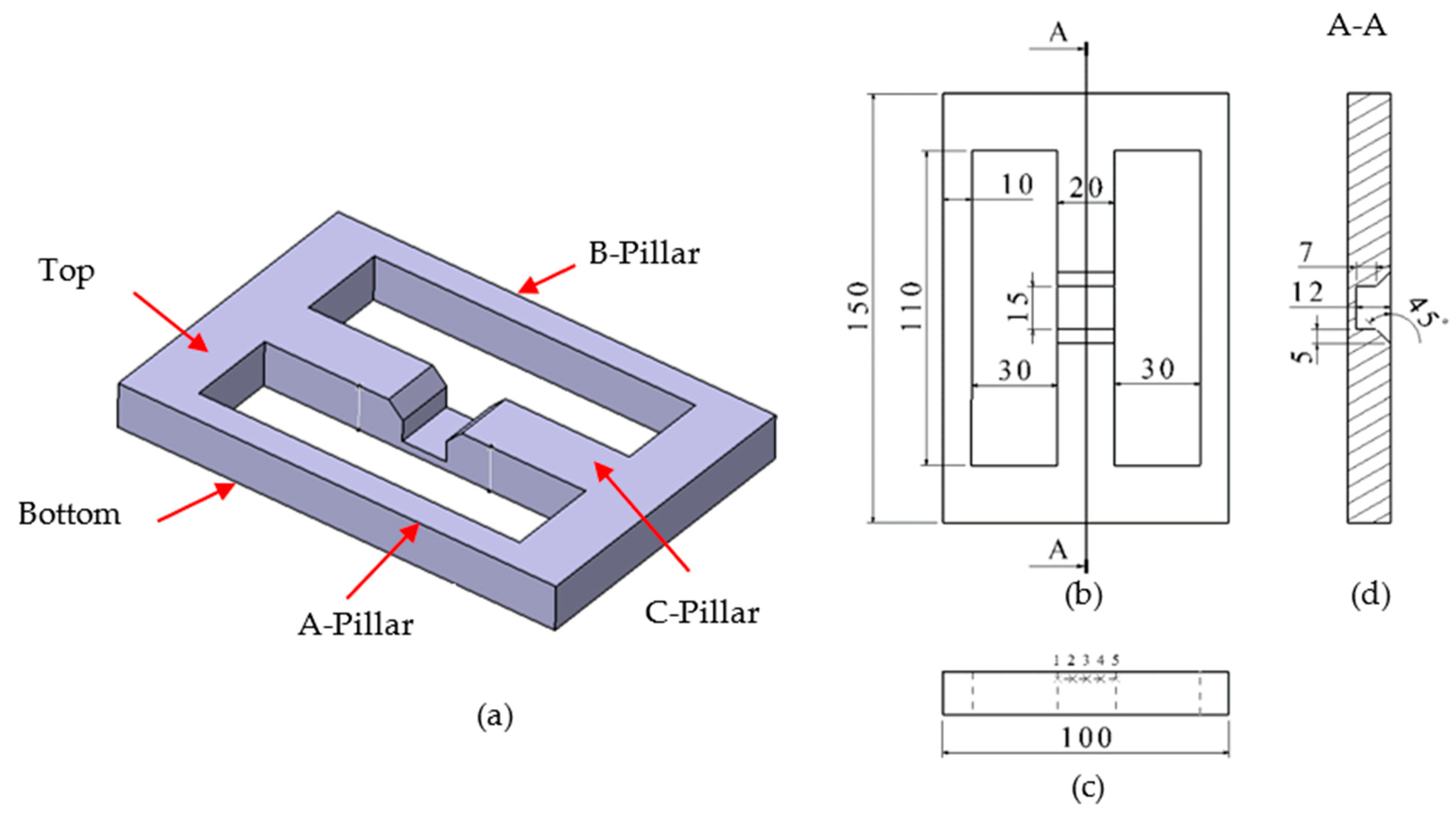
2.1. Material and Wire Arc Additive Manufacturing Parameters

Annealed 1045 steel was used as the substrate, and its chemical composition is presented in Table 1. The specimen was cut into pieces with the dimensions of 150 mm × 100 mm × 15 mm and had two 10 mm side pillars and one 20 mm pillar in the middle area, created via electric discharge machining (EDM) cutting. The three pillars were named the A-pillar, B-pillar, and C-pillar, as shown in Figure 1. A “V” groove was cut in the middle of the C-pillar. The groove was filled with the welding alloy (AWS ER70S-6, diameter 1.2 mm) using the gas metal arc welding method. This type of specimen is called a stress frame. This component can clearly observe dimension changes that are influenced by interior stress. The composition of the welding wire is shown in Table 2. The shielding gas was a mixture of 18% CO2 and 82% Ar with a flow rate of 15 L/min. The welding process was controlled through a robot controller (ABB Group Co., Ltd., Zurich, Switzerland) connected to a robot actuator and the welding power supply (Lorch, Auenwald, German). The ABB RAPID code contained the movement and welding instructions. The welding voltage was 18.9 V, the welding current was 117 A, the welding speed was 8 mm/s, and the wire-feeding speed was 3.0 m/min. The width of a single welding bead was 10 mm, and the height of the welding pass was 3 mm. Four layers were deposited in the groove, and an idle time of 1 min between each layer was employed to alleviate the heat accumulation. The weld path is shown in Figure 2. During the deposition process, the stress frame was unconstrained so that it could deform freely.

2.2. The Electroshock Treatment

The EST experiments were conducted using a self-made electroshock generator under room temperature conditions (20 ℃). The two ends of the C-pillar were clamped with the electrode of the electroshock generator so that the electromagnetic pulse could pass through the stress frame, as shown in Figure 3a. The schematic diagram of the EST device is shown in Figure 3b. The EST device consists of a trigger circuit, a switch, some introduction coils, some iron cores, an oscilloscope, and two copper electrodes. This device can convert high voltage to low voltage and high current. It provides a continuous electrical pulse to the metal sample through the oscilloscope, a reasonable setting for electrical pulse parameters, such as current size and pulse number. The specimen moved from the A-pillar to the B-pillar via five different points. The five points were marked at equal intervals at the end of the C-pillar, as shown in the top view provided in Figure 1c. The three specimens were treated using electroshocks with different processing parameters, as listed in Table 3. The sample was processed by AC pulse from the electroshock generator, with an electroshock pulse frequency of 50 Hz. The duration time of each EST was 10 s. After each EST, the sample was moved to the next point. The increase in the temperature of the specimens caused by joule heating during EST was measured using an infrared camera (Fotric 226, Fotric Intelligent Technology Co., Ltd., Shanghai, China).

2.3. Test Experiments

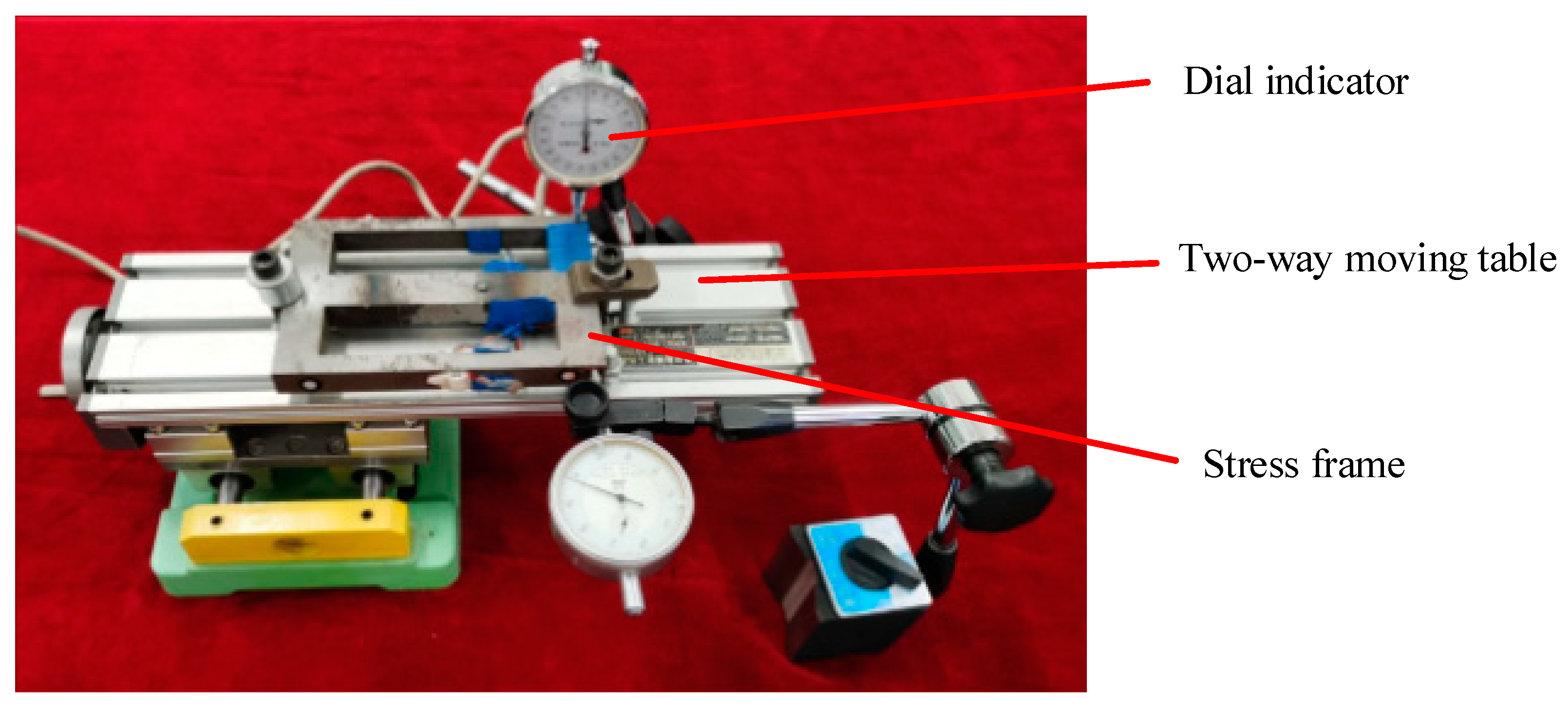
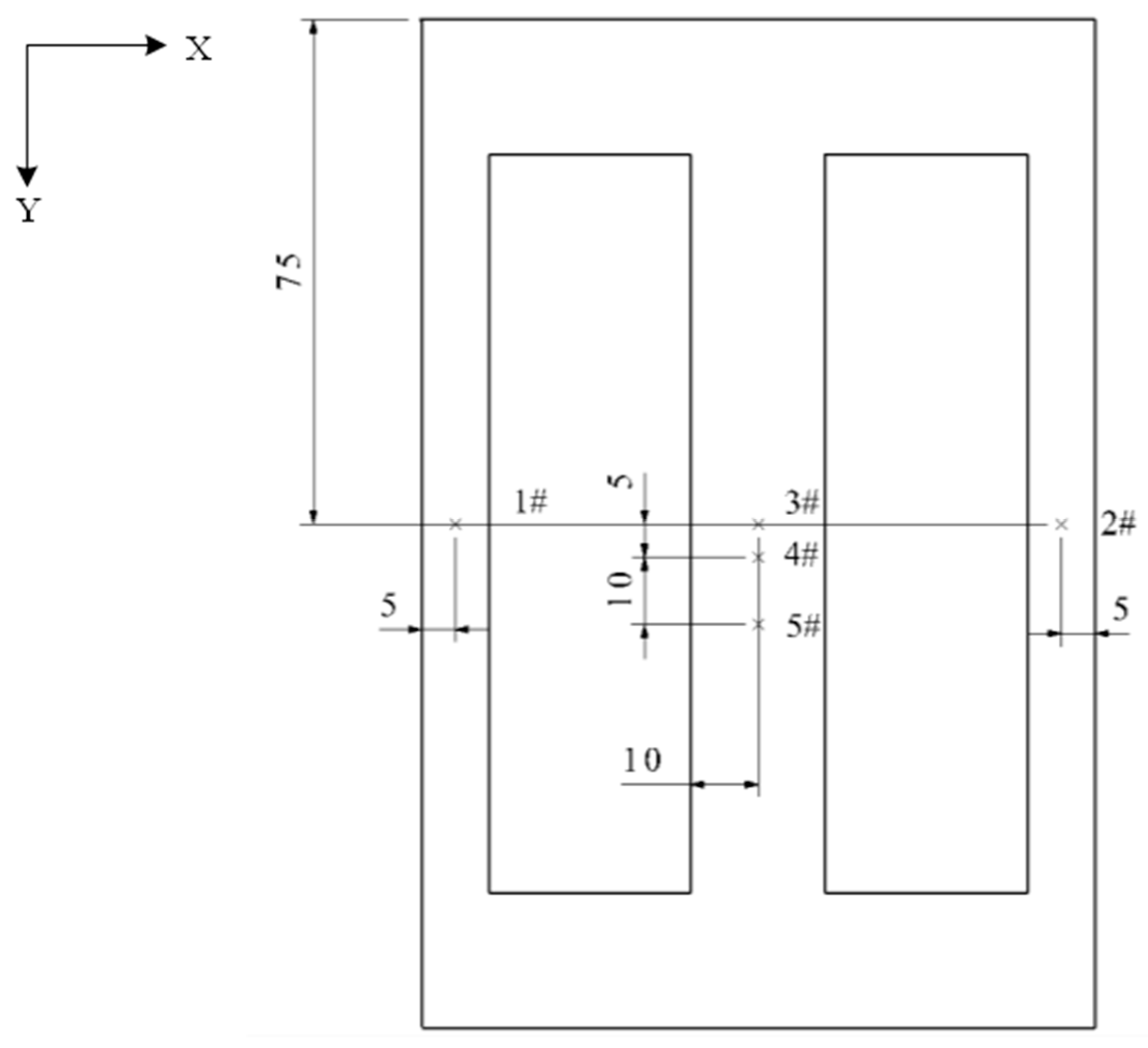
2.3.1. Measurement of Dimension

After material filling using wire arc additive manufacturing, serious deformation was observed in the stress frame due to the uneven thermal distribution. Three marking lines were made on the stress frame’s bottom of A-pillar, B-pillar, and C-pillar. The levelness of the frame was measured along the marking lines using a dial indicator (Chengdu Chengliang Tool Group Co., Ltd., Chengdu, China), a magnetic base (Harbin Measuring Cutting Tool Group Co., Ltd., Haer bin, China), and a bench (Askari Hardware Products Co., Ltd., Qingdao, China) after EDM cutting, after additive manufacturing, and after every group of EST, as shown in Figure 4. The accuracy of the dial indicator was 1 μm.

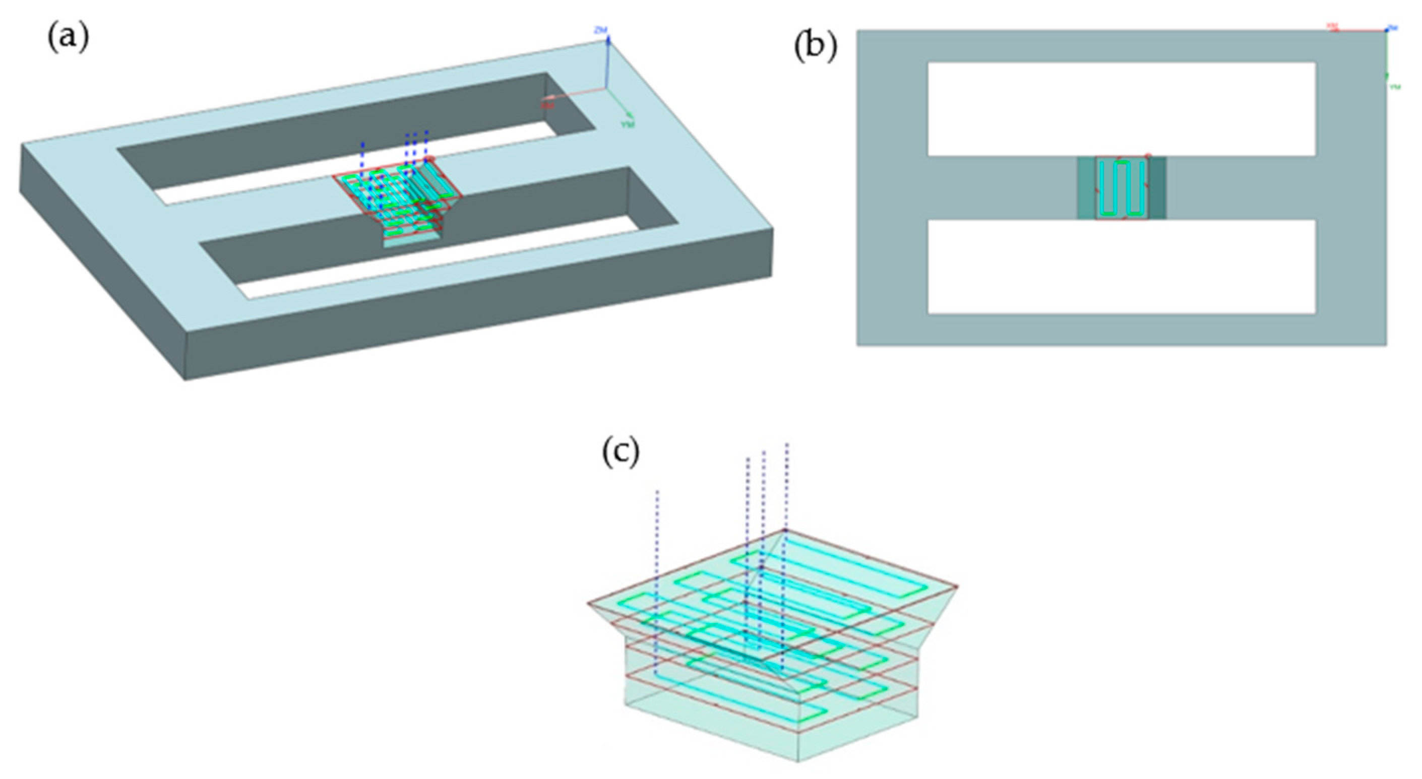
2.3.2. Characterization of Residual Stresses

Because specimen dimensions are closely related to residual stresses, the residual stresses of the key points of the stress frame should be measured after EDM cutting, additive manufacturing, and EST. Before every test of residual stress, 0.2 mm of the surface of stress measured points was removed via electrochemical corrosion in saturated sodium chloride solution. Residual stresses were evaluated via the XRD method using a residual stress tester (X-350A, Proto, Canada) with CrK α radiation (wavelength λ = 2.291 nm). The lattice plane (211) was adopted as the diffraction plane, and the scanning range ( 2 θ ) was recorded from 151° to 162° with a scan step size of 0.1°/step. The experimental results of the residual stresses were determined using the s i n 2   ϕ method [25]. The average values of the residual stresses were obtained based on three test points.

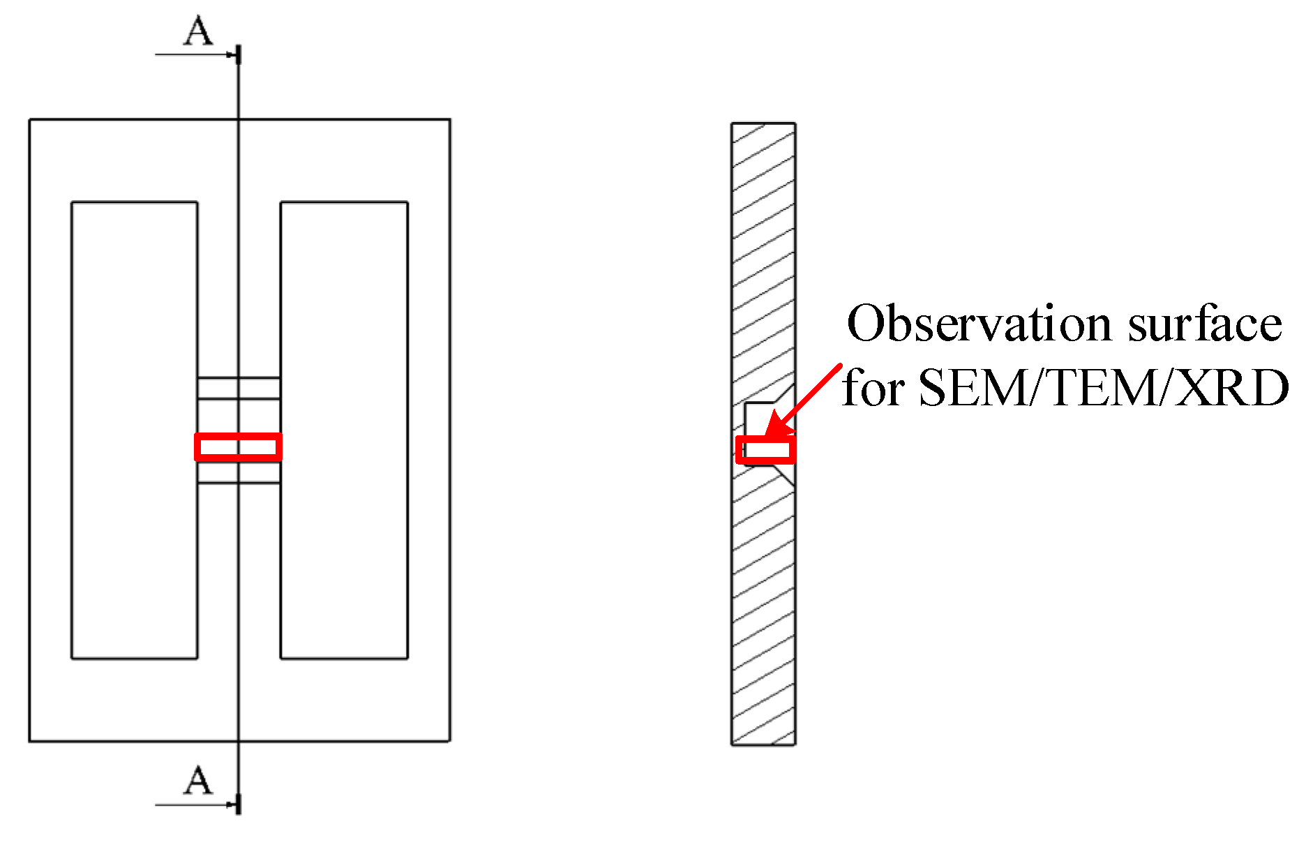
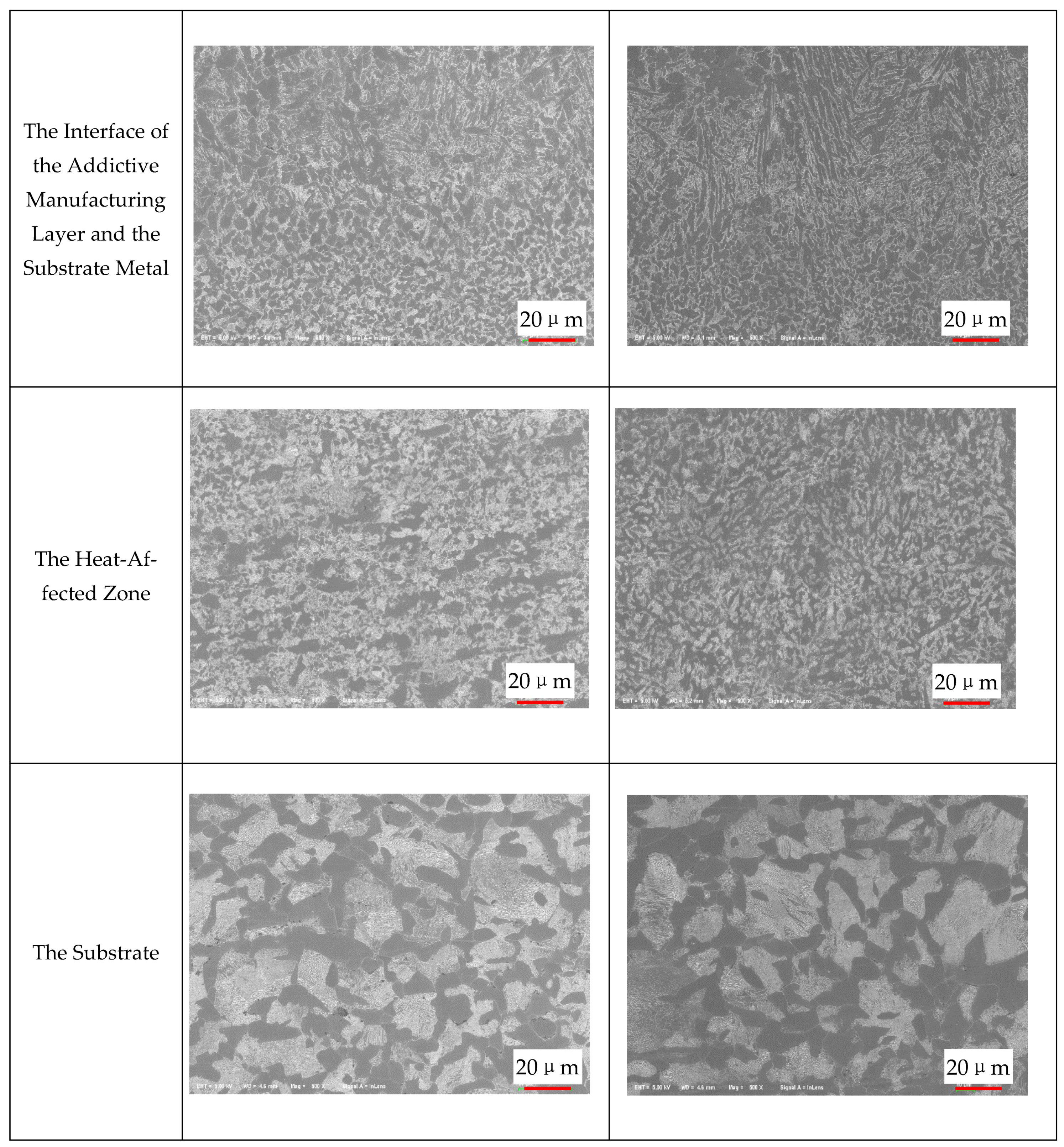
2.3.3. Characterization of Microstructure

In order to reveal the mechanism of residual stress decreasing induced by EST, the microstructures of the stress frame section were observed after additive manufacturing and after EST using a Zeiss field emission scanning electron microscope (Carl Zeiss AG, Oberkochen, German) and an X-Max 50 energy-dispersive X-ray spectrometer (Carl Zeiss AG, Oberkochen, German). The sampling and observation locations are shown in Figure 5. The acceleration voltage of the field emissions scanning electron microscope was 5 kV, the working distance was 4.6mm, and an InLens detector was used.
To observe the distribution of the internal dislocation by the scanning electron microscope, the sample was polished to 0.1 mm with sandpaper and then prepared using a twin-jet electro-polishing device (Deree micro Instrument Co., LTD, Suzhou, China) with a solution comprising 10% perchloric acid and 90% acetic acid at room temperature. A JEM-2100F transmission electron microscope (JEOL, Tokyo, Japan) with a working voltage of 200 kV was used for observation.
In order to investigate the dislocation density, X-ray diffraction (XRD) analysis was performed using a D/MAX-RB diffraction analyzer (Rigaku Corporation, Tokyo, Japan) at 12 kW. The scanning angle was 35°–105°, and the scanning speed was generally 1°/min.

3. Results and Discussion

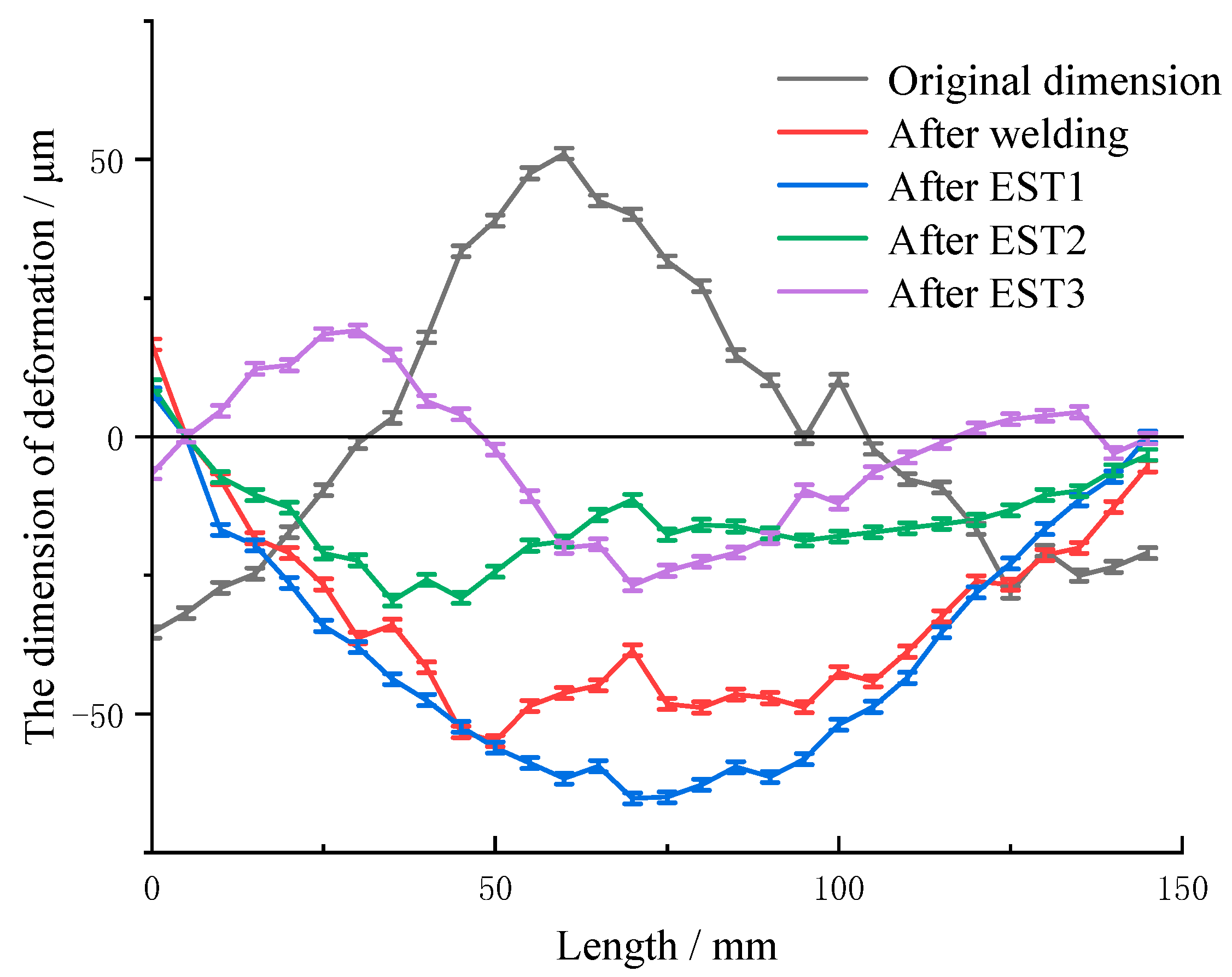
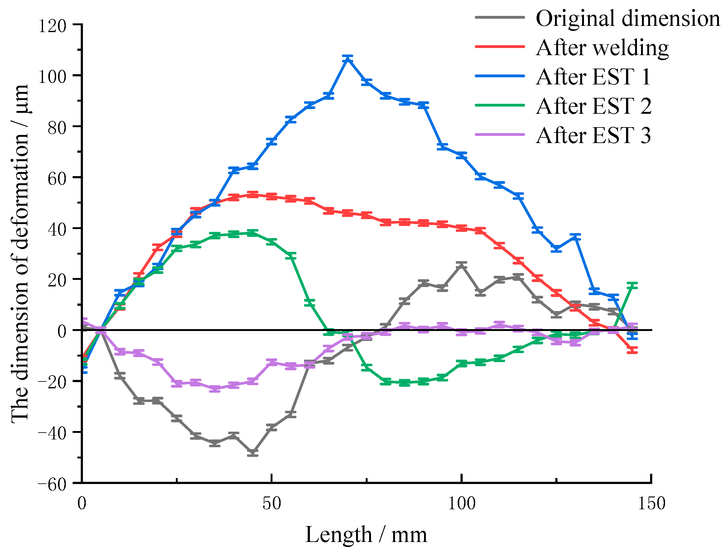
3.1. Effects of the Electroshock Temperature on the Geometric Dimensions

Figure 6 shows the three points in the stress frame, which are the key points for analysis. Figure 7 shows the temperature changes at three points of the frame, observed using the thermal imager when the equipment acted on points 1, 2, 3, 4, and 5 in sequence with the current at 110 A. The temperature at spot 1 resulted from contact with the positive electrode and rose the fastest. The temperature can rise by 40 °C within 3 s, but its area was very small. Once the electromagnetic pulse stopped, the temperature fell back down quickly. The temperature at spot 2 in the welding area rose gradually at a speed of 1.5 °C/s and increased from room temperature to 61.6 °C within 23 s, with a total increase of 40.2 °C. The temperature at spot 3 showed little change due to contact with the negative electrode, fluctuating between 25 °C and 35 °C.
Figure 8 shows the six lines on the stress frame, which are the key lines for analysis. The temperature variations on lines 1, 2, and 3 observed using the thermal imager are shown in Figure 9. The length of the stress frame is shown on the X-axis. The temperatures of line 1, 2 and 3 at some point are shown on the Y axis. At the area near the electrode, the temperature was high and changed rapidly. The temperature at the positive electrode was 36.5 °C, and it gradually dropped to room temperature at the negative electrode. However, the groove area where the material was filled using the wire arc additive manufacturing method was a special area. The temperature of the additive area where the C-pillar was located was the highest at 48 °C.
The temperature changes on lines 4, 5, and 6 observed using the thermal imager are shown in Figure 10. The width of the stress frame is shown on the X-axis. The temperature of lines 4, 5 and 6 at some point are shown on the Y-axis. The temperature distribution curves showed that the temperature of the additive area was the highest, whereas the temperatures of the A-pillar and B-pillar were lower. Because W = U 2 / R , where U is the voltage acting at two ends of the specimen, and R is the material’s resistance. During EST, the voltage U was the same, and the resistance of the C-pillar was smaller than that of the A-pillar and B-pillar. The inner side temperatures of the A-pillar and B-pillar in the stress frame were higher than the temperatures on the outer side. The current favors the shorter path, so temperatures of the inner side of the A-pillar and B-pillar were higher.
Through carrying out electroshock treatment on the additively manufactured component, the temperature of the stress frame increases because of EST was observed. However, the maximum temperature was 61.6 °C, which was not enough to result in phase changes in the material. The effect of EST on the component was non-thermal. The resistance at the additive area was smaller than at the substrate, resulting in higher temperature there than in other areas.

3.2. Geometric Dimension Analysis of the Stress Frame

The levelness of the three pillars in the stress frame was a focus of the present study because obvious warping was observed. After EDM cutting, the levelness of the pillars was in a fundamentally horizontal state. After additive manufacturing, the middle of the back of the C-pillar bulged to 217.9 μ m . After electroshock treatment, the deformation at the back of the C-pillar decreased from 217.9 μ m to 172.2 μ m . This is shown in Figure 11. Because plastic deformation was generated in the C-pillar, few deformation changes were observed after applying EST.
The A-pillar and B-pillar were leveled after EDM cutting, as shown in Figure 12 and Figure 13. After additive manufacturing, large deformation and serious warpage could be observed at the backs of the pillars. The maximum deformation was −54.9 μ m and 53.2 μ m , respectively. After the first electroshock treatment, the deformation was more serious, increasing to −65.2 μ m and 106.6 μ m , respectively. After the second electroshock treatment, the deformation of the two pillars and the warpage gradually decreased. After the third electroshock treatment, the levelness of the two pillars was restored to its original state before additive manufacturing.
The experimental results show that electroshock treatment can effectively improve components’ geometric dimensions and eliminate the deformation produced through processing.

3.3. Influence of Residual Stress on Geometrical Dimensions

In order to research the effect of the EST mechanism on the component geometric dimensions, the stress frame residual stress was tested after EDM cutting, after additive manufacturing, and after EST. Figure 14 shows the X-ray diffraction test points. Table 4 shows the test point residual stress results along the stress frame’s Y-axis. The following observations were made based on the test results. After additive manufacturing, the residual stress of the C-pillar increased, and the residual stress of the A-pillar and B-pillar decreased. It was speculated that compressive stress was generated in the C-pillar for additive manufacturing. At the same time, tensile stress was generated in the A-pillar and the B-pillar. In the C-pillar, the residual stress gradually decreased from the middle to the end. The residual stress values at point 3, point 4, and point 5 were 303 Mpa, 228 Mpa, and 203 Mpa, respectively, and the biggest residual stress caused by additive manufacturing was observed in the middle.
According to the changes in the residual stress, it was found that residual stress decreased in different degrees after EST. The average reduction was 127.6 Mpa, the maximum reduction was 156 Mpa, and the minimum reduction was 101 Mpa. It can be inferred that the geometric dimensions of the stress frame were related to the release of residual stress in the component via EST. The stress frame warped as the residual stress increased. As the residual stress was released, the levelness of the stress frame would improve.
The stress frame was cut from a large steel sheet, and the test point 2# was on the side of the steel sheet. The residual stress on the steel sheet side was decreased due to natural aging. The test point 1# was located in the inner section of the large steel sheet. There was little natural aging in the inner section. Although the residual stress values of points 1# and 2# before additive manufacturing were different, the residual stress values of both points decreased after additive manufacturing. After EST, points 1# and 2# residual stress values were close and uniform.

3.4. Effects of the Microstructure of EST on Geometric Dimensions

The morphologies of the welding area after additive manufacturing and after EST are shown in Figure 15. The top of the additive manufacturing layer exhibited coarse column-like grains. The grains in the middle of the additive manufacturing layer were fine. The interface of the additive manufacturing layer and the substrate was the bonding area of welding. Column-like grains and fine grains were observed in the bond area at the same time. Fine ferrite and pearlite were observed in the heat-affected zone and large-grained in the substrate. These are typical microstructural diagrams observed in welding.
By comparing the micrographs taken after additive manufacturing and after EST, it was found that there were no obvious changes in the microstructure in any of the welding areas. Because the samples’ maximum temperature reached only 100 °C during EST, it did not meet the phase transformation temperature of steel 45. Therefore, this implies that the change in the residual stress had nothing to do with the change in the microstructure after EST.

3.5. Effects of EST on Dislocations

Based on the TEM morphology of the welding area observed after additive manufacturing and after EST, as shown in Figure 16, we found that dislocation pile-up was relieved, and the dislocation distribution was more uniform. When the current pulse passes through the metal material, a mass of free electrons with directional drift is generated. The continuous directional collision between free electrons and atoms generates an external electron wind inside the material. Dislocations are moved, the dislocation density is reduced, the dislocation nodule is opened, the dislocation slipped, the dislocation plug degree is reduced, and the dislocations show a uniform distribution resulting from electron wind.
The relationship between the residual stress σ i and dislocation density ρ is as follows [26,27]:
σ i = σ 0 + M ¯ α G b ρ
where σ 0 is the stress constant, M ¯ is the mean Taylor coefficient, α is a constant, and G is the shear modulus. It can be seen from the formula that there is a linear relationship between residual stress σ i and dislocation density ρ .
For isotropic materials, the dislocation density caused by X-ray peak broadening follows the Williamson-Hall [28] equation:
K α s D + N ρ   K
where K is the peak width, N is a constant, α s is the shape factor, D is the grain size, K = 2 s i n θ λ is the diffraction vector, θ is the diffraction angle, and λ is the diffraction wavelength.
The XRD diffraction spectrum diagrams obtained after additive manufacturing and EST are shown in Figure 16. After EST, the peak width narrowed, which represents the dislocation density. According to the Lorentz-fitted curves of the (110) α diffraction peak (inserted in Figure 17), the FWHM values of the diffraction peak after additive manufacturing and after EST could be measured as 0.318° and 0.299°, respectively. The dislocation density after additive manufacturing and EST were calculated as 5.251 × 10¹⁵ m−2 and 4.612 × 10¹⁵ m−2 using the WH method. These results indicate that EST decreased the dislocation density. This results in the residual stress being reduced, ensuring the geometric dimensions of the component.

4. Conclusions

This study investigates the influence of EST on the microstructure, residual stress, and geometric dimensions of components created via additive manufacturing. The following conclusions can be drawn from our findings.
(1)
After EST, the levelness of the stress frame was basically restored. The residual stress of the additively manufactured components was reduced by 127.6 MPa through EST. The geometric dimensions were ensured for the reduction in the residual stress.
(2)
According to SEM and TEM results, the dislocation density of the stress frame in the addictive manufacturing area was reduced, and the dislocation distribution was more homogeneous after EST. This was the reason for the decrease in residual stress and the improvement in the geometric dimensions. At the same time, the microstructure of the stress frame did not change.
(3)
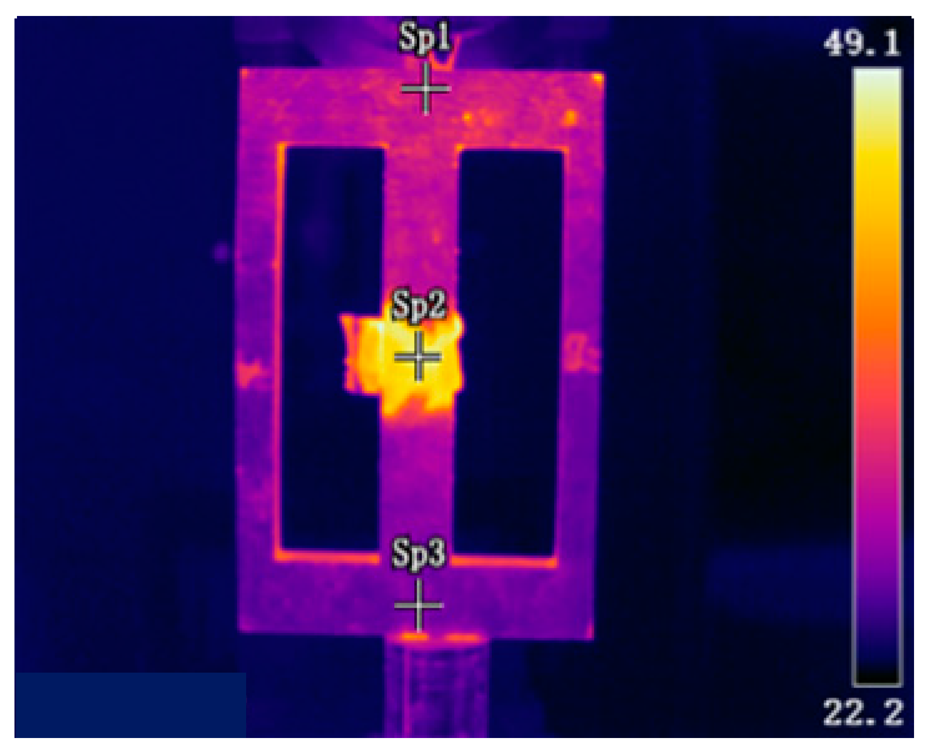
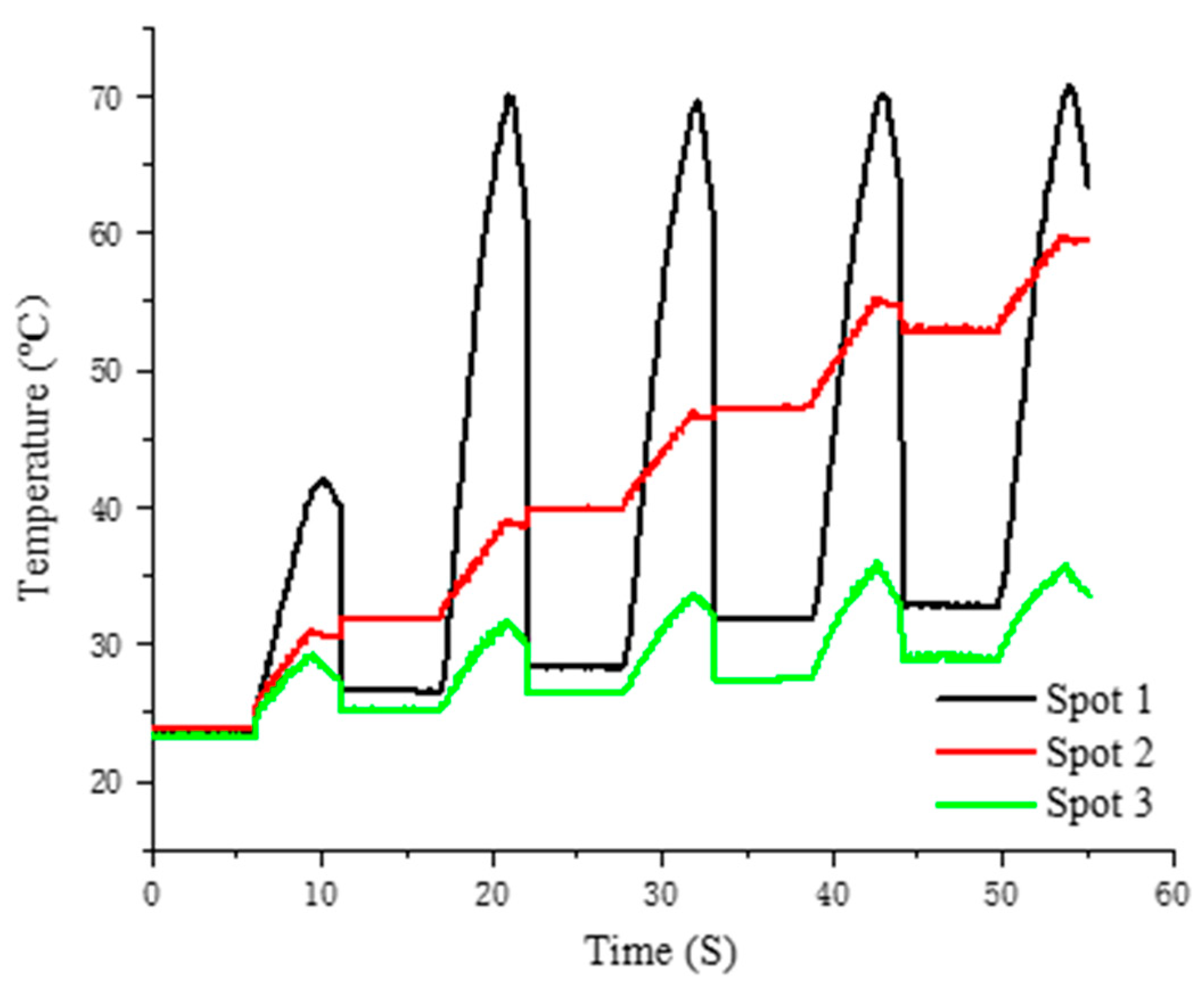
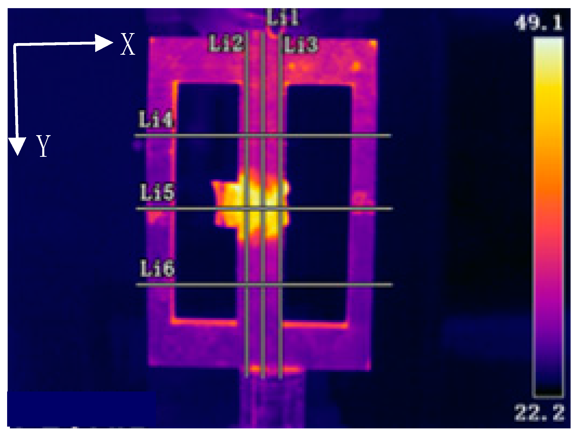
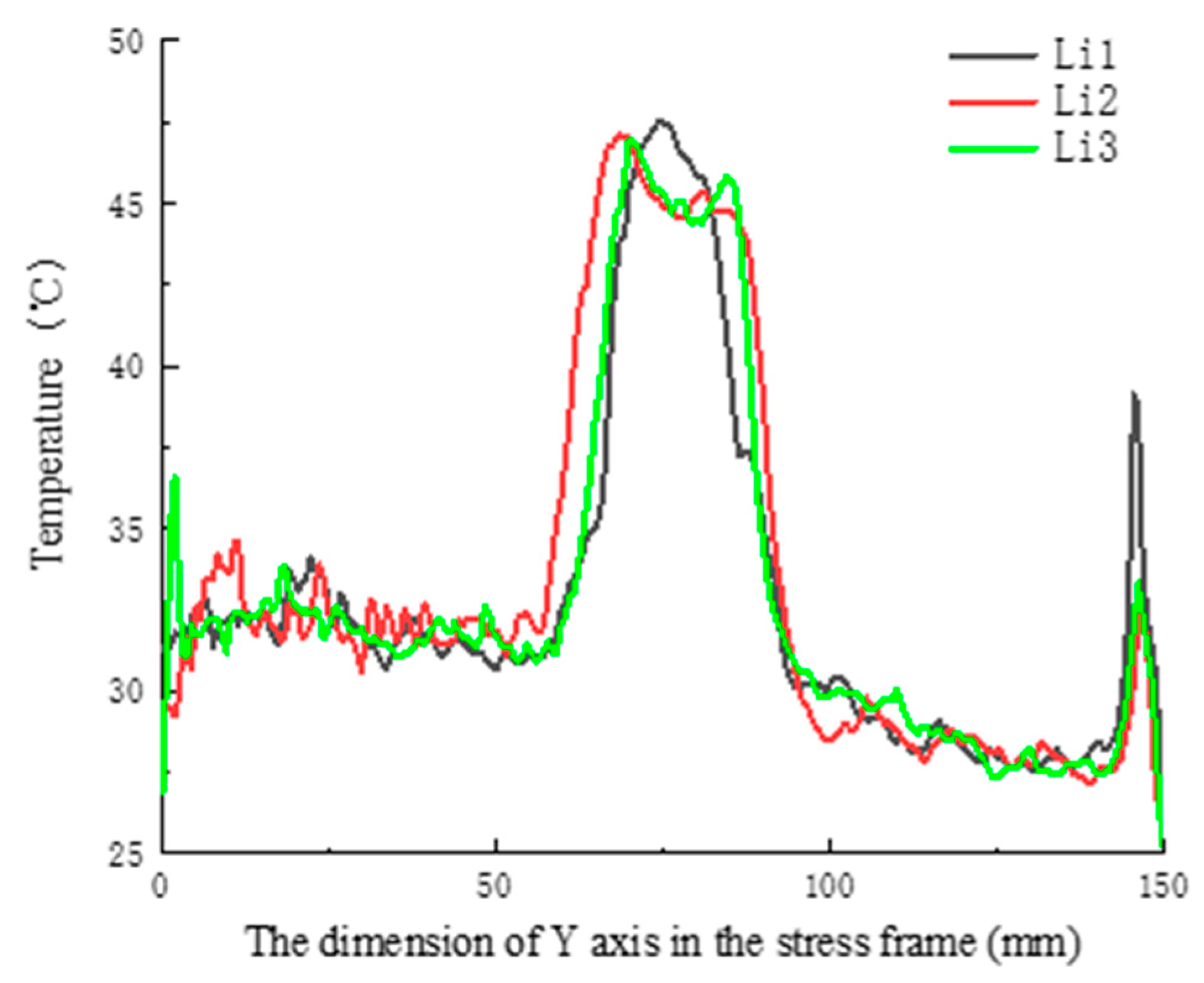
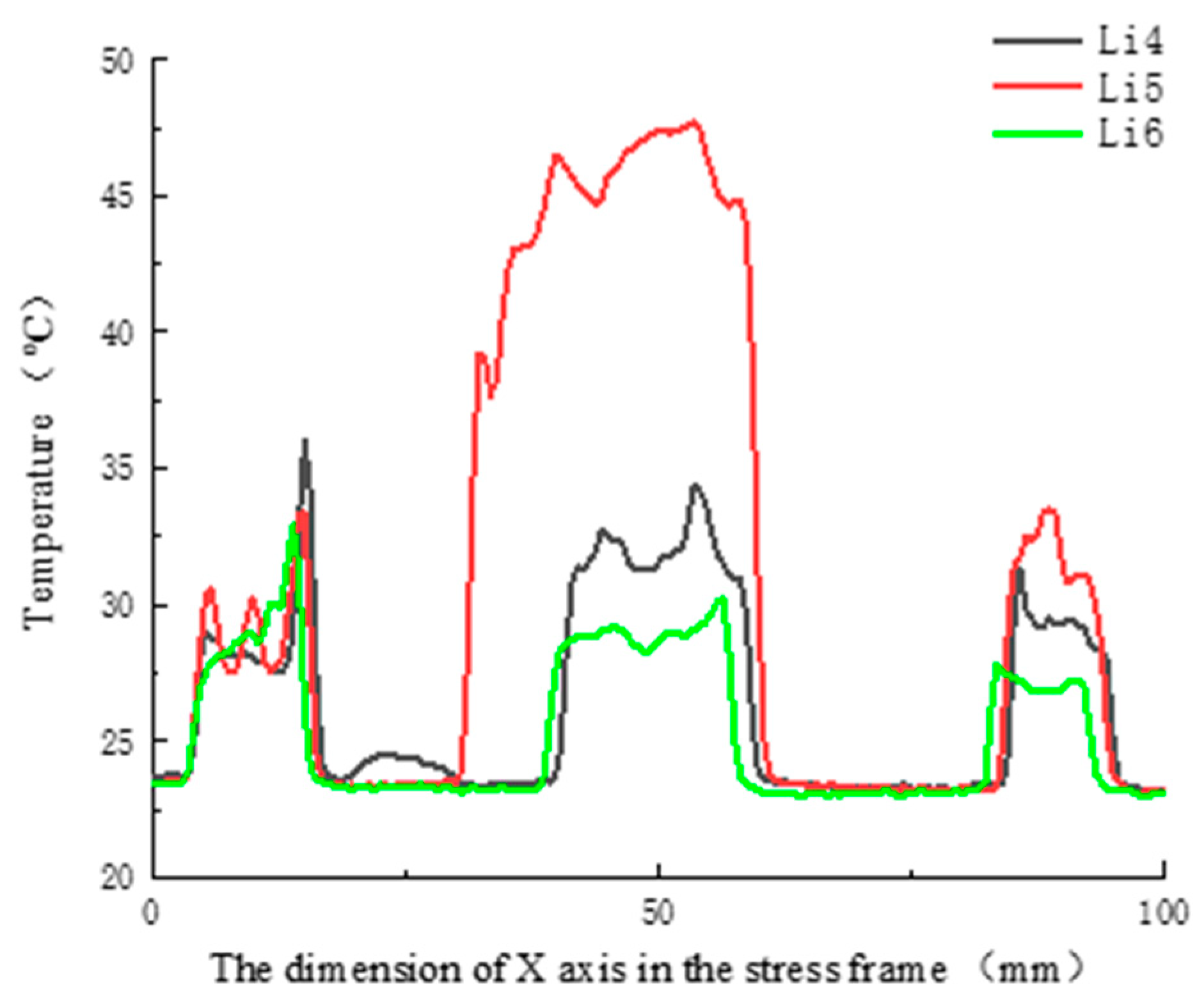
When the additively manufactured stress frames samples were processed via EST, the temperature of the middle part of the C-pillar was the highest because the microstructure at this area forming during WAAM was different from the substrate, and the EST process further altered the interior structure. The temperature of the substrate in the C-pillar was lower. The substrate temperature decreased gradually under the electroshock pulse when moving from the positive to the negative electrode.

Author Contributions

M.W.: formal analysis, writing–original draft; Z.H.: writing–review & editing; X.Q.: funding acquisition, project administration, supervision. All authors have read and agreed to the published version of the manuscript.

Funding

This paper was supported by the National Key Research and Development Program (No. 2018YFB1106503), the Important Science and Technology Innovation Program of Hubei province (No. 2018AAA021), and the Innovative Research Team Development Program of the Ministry of Education of China (No. IRT17R83).

Institutional Review Board Statement

Not applicable.

Informed Consent Statement

Not applicable.

Data Availability Statement

Not applicable.

Conflicts of Interest

The authors declare no conflict of interest.

References

  1. Klocke, F.; Arntz, K.; Teli, M.; Winands, K.; Wegener, M.; Oliari, S. State-of-the-art laser additive manufacturing for hot-work tool steels. Procedia CIRP 2017, 63, 58–63. [Google Scholar] [CrossRef]
  2. Murathan Kalender, Y.B.; Ersoy, S.; Salman, S. Additive manufacturing and 3d printer technology in aerospace industry. J. Aeronaut. Space Technol. 2020, 13, 10. [Google Scholar]
  3. Shen, X.; Gao, K.; Dong, S. Simulation and analysis of electron beam welding residual stress in thin-walled high-temperature alloy aeroengine structures. Int. J. Adv. Manuf. Technol. 2020, 107, 3953–3966. [Google Scholar] [CrossRef]
  4. AMondal, A.K.; Lohit, A.; Biswas, P.; Bag, S.; Das, M. Prediction of weld-induced distortion of large structure using equivalent load technique. Proc. Inst. Mech. Eng. Part B J. Eng. Manuf. 2016, 232, 499–512. [Google Scholar] [CrossRef]
  5. Yilmaz, A.F.; Günay, M. Investigation of Mechanical strength and distortion in submerged arc welding of ah36 ship steel plate. J. Ship Prod. Des. 2017, 33, 335–341. [Google Scholar] [CrossRef]
  6. Rathinasuriyan, C.; Kumar, V.S.S. Experimental investigation of weld characteristics on submerged friction stir welded 6061-T6 aluminum alloy. J. Mech. Sci. Technol. 2017, 31, 3925–3933. [Google Scholar] [CrossRef]
  7. Akhtar, N.; Afzal, M.; Khan, M.A.; Hussain, M.; Ali, M.N. Assessment of cold deformation effects on yield-to-tensile ratio and dimensional stability of an aluminium alloy extruded tube. In Proceedings of the 2017 14th International Bhurban Conference on Applied Sciences & Technology (IBCAST), Islamabad, Pakistan, 10–14 January 2017; pp. 29–33. [Google Scholar]
  8. Song, Y.; Ding, X.; Xiao, L.; Zhao, X.; Cai, Z.; Guo, L.; Li, Y.; Zheng, Z. Effects of two-stage aging on the dimensional stability of Al-Cu-Mg alloy. J. Alloys Compd. 2017, 701, 508–514. [Google Scholar] [CrossRef]
  9. Tu, X.; Xiao, L.; Zhao, X.; Cai, Z.; Peng, Z.; Wei, D. Effects of thermal-cold cycling on the dimensional stability of TiC reinforced steel matrix composite. Mater. Lett. 2020, 279, 128483. [Google Scholar] [CrossRef]
  10. Singla, A.K.; Singh, J.; Sharma, V.S. Processing of materials at cryogenic temperature and its implications in manufacturing: A review. Mater. Manuf. Process. 2018, 33, 1603–1640. [Google Scholar] [CrossRef]
  11. Guo, H.; Zeng, X.; Fan, J.; Zhang, H.; Zhang, Q.; Li, W.; Dong, H.; Xu, B. Effect of electropulsing treatment on static recrystallization behavior of cold-rolled magnesium alloy ZK60 with different reductions. J. Mater. Sci. Technol. 2019, 35, 1113–1120. [Google Scholar] [CrossRef]
  12. Räbiger, D.; Zhang, Y.; Galindo, V.; Franke, S.; Willers, B.; Eckert, S. The relevance of melt convection to grain refinement in Al–Si alloys solidified under the impact of electric currents. Acta Mater. 2014, 79, 327–338. [Google Scholar] [CrossRef]
  13. Yiu, P.; Chen, Y.; Chu, J.; Chang, S.; Bei, H.; Jang, J.; Hsueh, C. Rapid relaxation and embrittlement of Zr-based bulk metallic glasses by electropulsing. Intermetallics 2013, 34, 43–48. [Google Scholar] [CrossRef]
  14. Kim, M.-J.; Lee, K.; Oh, K.H.; Choi, I.-S.; Yu, H.-H.; Hong, S.-T.; Han, H.N. Electric current-induced annealing during uniaxial tension of aluminum alloy. Scr. Mater. 2014, 75, 58–61. [Google Scholar] [CrossRef]
  15. Pan, L.; Wang, B.; Xu, Z. Effects of electropulsing treatment on residual stresses of high elastic cobalt-base alloy ISO 5832-7. J. Alloys Compd. 2019, 792, 994–999. [Google Scholar] [CrossRef]
  16. Pan, L.; He, W.; Gu, B. Effects of electric current pulses on mechanical properties and microstructures of as-quenched medium carbon steel. Mater. Sci. Eng. A 2016, 662, 404–411. [Google Scholar] [CrossRef]
  17. Xiang, S.; Zhang, X. Dislocation structure evolution under electroplastic effect. Mater. Sci. Eng. A 2019, 761, 138026. [Google Scholar] [CrossRef]
  18. Wang, F.; Qian, D.; Hua, L.; Mao, H.; Xie, L. Voids healing and carbide refinement of cold rolled M50 bearing steel by electropulsing treatment. Sci. Rep. 2019, 9, 11315. [Google Scholar] [CrossRef]
  19. Yang, C.L.; Yang, H.J.; Zhang, Z.J.; Zhang, Z.F. Recovery of tensile properties of twinning-induced plasticity steel via electropulsing induced void healing. Scr. Mater. 2018, 147, 88–92. [Google Scholar] [CrossRef]
  20. Song, X.; Wang, F.; Qian, D.; Hua, L. Tailoring the residual stress and mechanical properties by electroshocking treatment in cold rolled M50 steel. Mater. Sci. Eng. A 2020, 780, 139171. [Google Scholar] [CrossRef]
  21. Xie, L.; Liu, C.; Song, Y.; Guo, H.; Wang, Z.; Hua, L.; Wang, L.; Zhang, L.-C. Evaluation of microstructure variation of TC11 alloy after electroshocking treatment. J. Mater. Res. Technol. 2020, 9, 2455–2466. [Google Scholar] [CrossRef]
  22. Xie, L.; Guo, H.; Song, Y.; Liu, C.; Wang, Z.; Hua, L.; Wang, L.; Zhang, L.-C. Effects of electroshock treatment on microstructure evolution and texture distribution of near-β titanium alloy manufactured by directed energy deposition. Mater. Charact. 2020, 161, 110137. [Google Scholar] [CrossRef]
  23. Jung, J.; Ju, Y.; Morita, Y.; Toku, Y. Enhancement of fatigue life of aluminum alloy affected by the density of pulsed electric current. Int. J. Fatigue 2017, 103, 419–425. [Google Scholar] [CrossRef]
  24. Liang, C.-L.; Lin, K.-L. The microstructure and property variations of metals induced by electric current treatment: A review. Mater. Charact. 2018, 145, 545–555. [Google Scholar] [CrossRef]
  25. Balc, N.; Strnad, G.; Cazacu, R.; Chetan, P.; Gaz Florea, A.S.; Peti, F. Effect of phosphate/fluoride electrolytes on mass and dimensional stability of anodization bath manufactured by FDM. MATEC Web Conf. 2017, 137, 02012. [Google Scholar]
  26. Kocks, U.F. Laws for work-hardening and low-temperature creep. J. Eng. Mater. Technol. 1976, 98, 76–85. [Google Scholar] [CrossRef]
  27. Mecking, H.; Kocks, U.F. Kinetics of flow and strain-hardening. Acta Metall. 1981, 29, 1865–1875. [Google Scholar] [CrossRef]
  28. Williamson, G.K.; Hall, W.H. X-ray line broadening from filed aluminium and wolfram. Acta Metall. 1953, 1, 22–31. [Google Scholar] [CrossRef]
Figure 1. Sketch of the specimen (mm). (a) Isometric view; (b) Front view; (c) Top view; (d) Section view.
Metals 12 01434 g001
Figure 2. Sketch of weld path. (a) Whole welding path from isometric view; (b) Welding path at first layer from the top view; (c) Whole welding path without substrate.
Metals 12 01434 g002
Figure 3. (a) Specimen treated with EST; (b) Schematic of the EST device.
Metals 12 01434 g003
Figure 4. Measurements of levelness at the bottom of the stress frame.
Metals 12 01434 g004
Figure 5. Sketch of the specimen location for SEM/TEM/XRD.
Metals 12 01434 g005
Figure 6. Observation points for temperature during EST.
Metals 12 01434 g006
Figure 7. Temperature variation in observation points during EST.
Metals 12 01434 g007
Figure 8. Observation lines for temperature during EST.
Metals 12 01434 g008
Figure 9. Temperature distribution graph of line 1, line 2, and line 3.
Metals 12 01434 g009
Figure 10. Temperature distribution graph of line 4, line 5, and line 6.
Metals 12 01434 g010
Figure 11. Levelness changes at the bottom of the C-pillar.
Metals 12 01434 g011
Figure 12. Levelness changes at the bottom of the A-pillar.
Metals 12 01434 g012
Figure 13. Levelness changes at the bottom of the B-pillar.
Metals 12 01434 g013
Figure 14. X-ray diffraction test points (mm).
Metals 12 01434 g014
Figure 15. Morphology of the welding area after additive manufacturing and after EST.
Metals 12 01434 g015aMetals 12 01434 g015b
Figure 16. TEM morphology of the welding area after additive manufacturing and after EST. (a,b) After additive manufacturing; (c,d)After EST.
Metals 12 01434 g016
Figure 17. XRD diffraction spectrum diagram.
Metals 12 01434 g017
Table 1. Chemical composition of 1045 steel (wt. %).
CSiMnSP
0.42–0.500.17–0.370.50–0.80≤0.035≤0.035
Table 2. Chemical composition of welding wire (wt. %).
CMnSiNiCr
0.06–0.151.40–1.850.08-1.85≤0.15≤0.15
Table 3. EST processing parameters.
Group NumberEST NumberTreatment PositionCurrent Intensity/A
11170
2270
3370
4470
5570
26190
7290
8390
9490
10590
3111110
122110
133110
144110
155110
Table 4. The test results for residual stress in specimens.
Number of Test PointAfter EDM Cutting
/MPa
After Additive Manufacturing
/MPa
After Electroshock Treatment/MPa
1#21818676
2#23−137−14
3#234303165
4#18022872
5#171203102
Publisher’s Note: MDPI stays neutral with regard to jurisdictional claims in published maps and institutional affiliations.

