
Investigation of a Macromolecular Additive on the Decrease of the Aluminum Horizontal Etching Rate in the Wet Etching Process


Abstract
:1. Introduction
2. Experimental Section
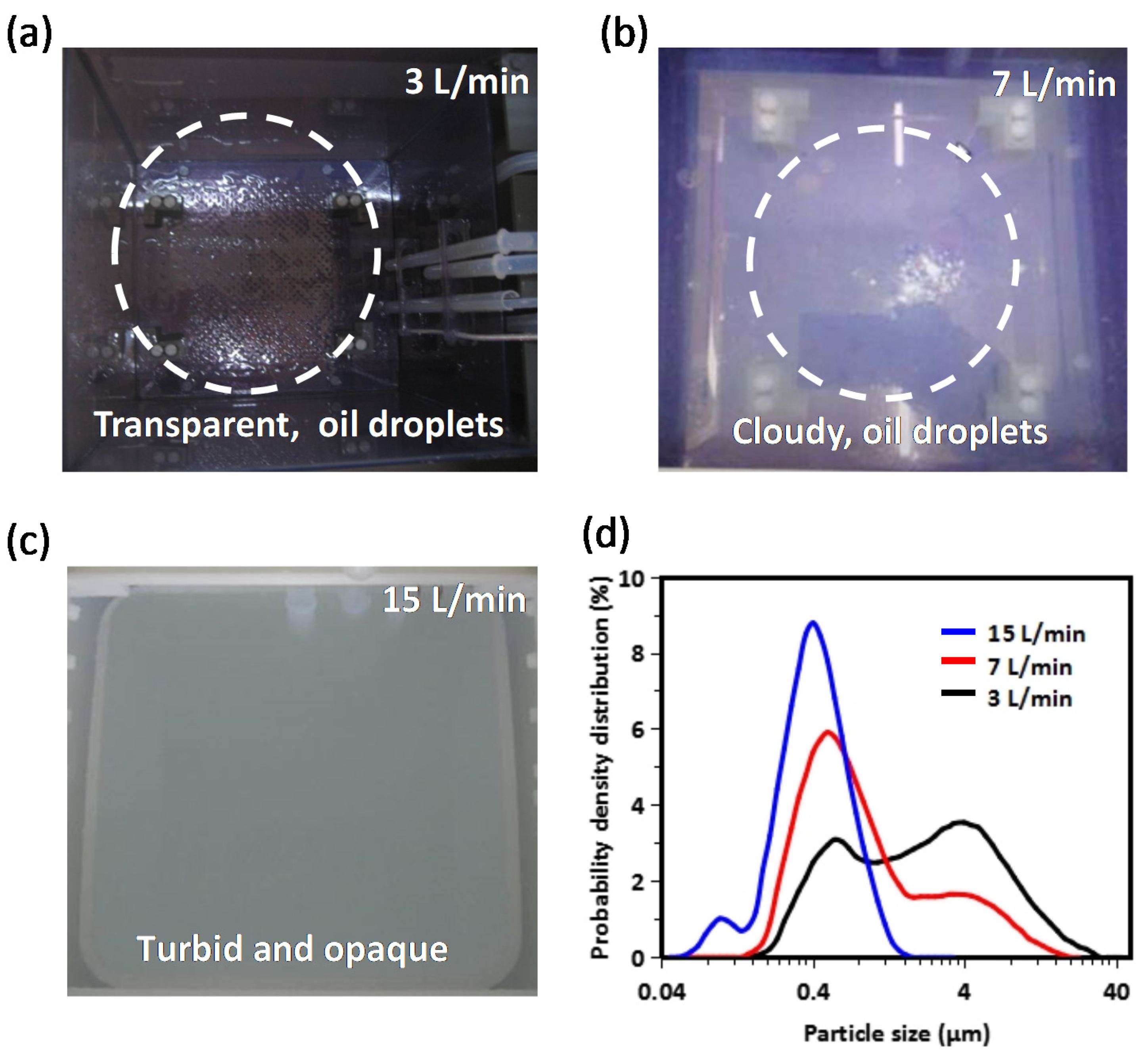
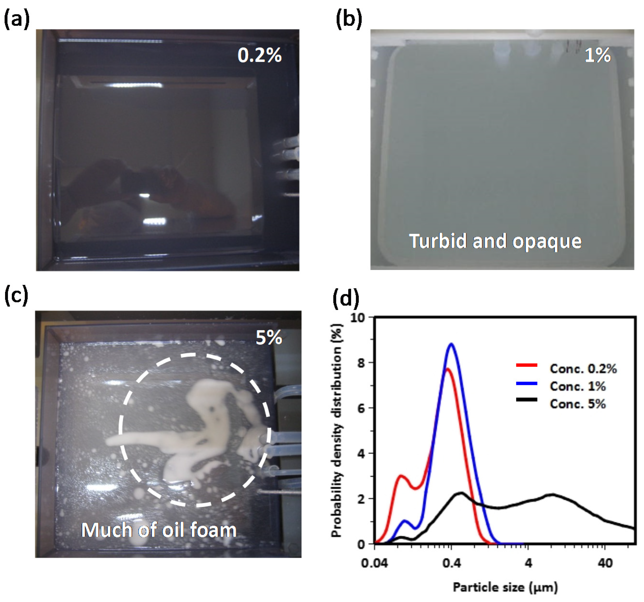
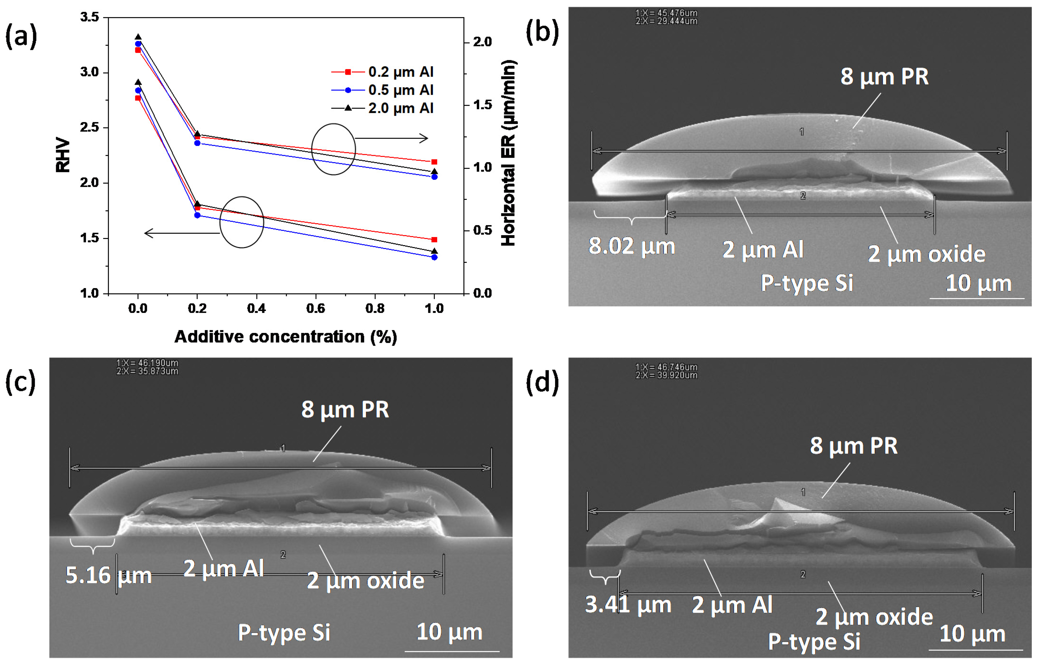
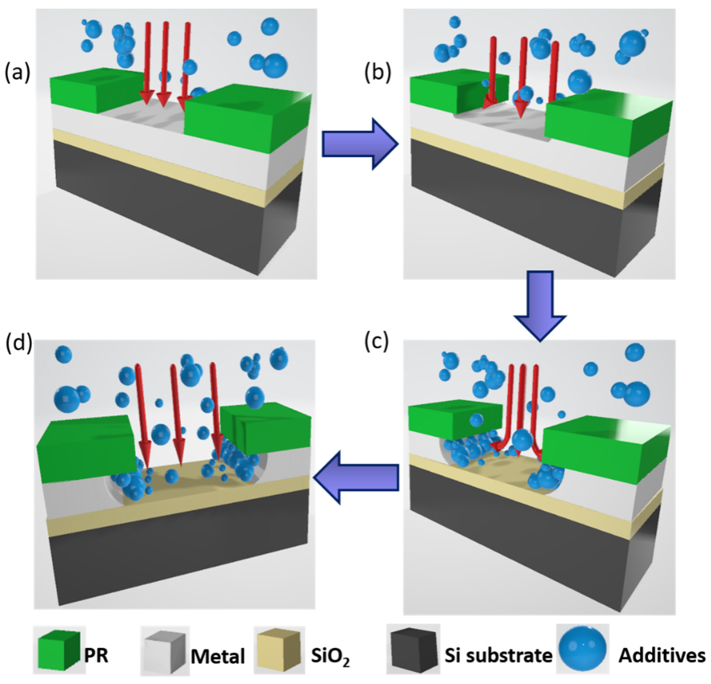
3. Results and Discussion
4. Conclusions
Author Contributions
Funding
Institutional Review Board Statement
Informed Consent Statement
Data Availability Statement
Acknowledgments
Conflicts of Interest
References
- Bhagwat, V.; Langer, J.P. A comparison of dry plasma and wet chemical etching of GaSb photodiodes. J. Electrochem. Soc. 2003, 5, 151. [Google Scholar] [CrossRef]
- Chatterjee, S.; Ujihara, M.; Lee, D.G.; Chen, J.; Lei, S.; Carman, G.P. Spray etching 2 μm features in 304 stainless steel. J. Micromech. Microeng. 2006, 16, 2585–2592. [Google Scholar] [CrossRef]
- Ren, P. The investigation to improve photo resistor adhesion on the metal aluminum surface. Appl. IC 2018, 35, 33–36. [Google Scholar]
- Majumdar, S.; Majumder, S.; Kakati, A. Effect of aluminum wet etching on GaAs and poly-dimethylsiloxane substrate: Surface morphology and topography analysis. Mater. Focus 2018, 7, 45–49. [Google Scholar] [CrossRef]
- Piragash, K.; Venkatesh, A.; Moorthy, V. Wet-chemical etching: A novel nanofabrication route to prepare broadband random plasmonic metasurfaces. Plasmonics 2019, 14, 365–374. [Google Scholar]
- Sharma, V.P.; Singh, S.J.; Shukla, R. Study of metal assisted chemical etching as an alternative to dry etching for the development of MEMS. In Proceedings of the International Conference on Precision, Meso, Micro and Nano Engineering, Indore, India, 12–14 December 2019; Volume 12, pp. 12–14. [Google Scholar]
- Hsu, C.E.; Li, W.C. Mitigating the insufficient etching selectivity in the wet release process of CMOS-MEMS metal resonators via diffusion control. J. Microelectromech. Syst. 2020, 29, 1415–1417. [Google Scholar] [CrossRef]
- GadelRab, S.M.; Miri, M.A.; Chamberlain, G.S. A comparison of the performance and reliability of wet-etched and dry-etched α-Si:H TFTs. IEEE Trans. Electron Devices 1998, 45, 560–563. [Google Scholar] [CrossRef]
- Karzhavin, Y.; Wu, W. Plasma induced charging and physical damage after dry etch processing. In Proceedings of the 3rd International Symposium on Plasma Process-Induced Damage, Honolulu, HI, USA, 4–5 June 1998; pp. 80–83. [Google Scholar]
- Han, Z. Power Semiconductor Device Based; Electronic Industry Press: Beijing, China, 2013. [Google Scholar]
- Seidel, H. The mechanism of an-isotropic, electrochemical silicon etching in alkaline solutions. In Proceedings of the IEEE 4th Technical Digest on Solid-State Sensor and Actuator Workshop, Head Island, SC, USA, 4–7 June 1990; pp. 80–92. [Google Scholar]
- Frank, W.E. Approaches for patterning of aluminum. Microelectron. Eng. 1997, 33, 85–100. [Google Scholar] [CrossRef]
- Lin, S.W.; Guo, L.H. Influence of metal layer thickness of spiral inductors on the quality factory by simulation. In Proceedings of the 5th International Conference on ASIC, Beijing, China, 21–24 October 2003; pp. 1115–1119. [Google Scholar]
- Scotti, G.; Kanninen, P.; Kallio, T.; Franssila, S. Bulk-aluminum microfabrication for micro fuel cells. J. Microelectromech. Syst. 2014, 23, 372–379. [Google Scholar] [CrossRef]
- Love, J.C.; Paul, K.E.; Whitesides, G.M. Fabrication of nanometer-scale features by controlled isotropic wet chemical etching. Adv. Mater. 2001, 13, 604–607. [Google Scholar] [CrossRef]
- Du, J.Q.; Liu, H.; Liu, W.G. Wet etching of aluminum periodic patterns in micrometer-scale. Adv. Mater. Res. 2013, 662, 117–121. [Google Scholar] [CrossRef]
- Jee, S.E.; Lee, P.S.; Yoon, B.J.; Jeong, S.H.; Lee, K.H. Fabrication of microstructures by wet etching of anodic aluminum oxide substrates. Chem. Mater. 2005, 17, 4049–4052. [Google Scholar] [CrossRef]
- Fricke, S.; Friedberger, A.; Schmid, U. The influence of plasma power on the temperature-dependent conductivity and on the wet chemical etch rate of sputter-deposited alumina thin films. Surf. Coat. Technol. 2009, 203, 2830–2834. [Google Scholar] [CrossRef]
- Jiang, Y.H. Chip manufacture thick aluminum etching process. Microprocessors 2016, 3, 23–24. [Google Scholar]
- Brask, J.K. Method for Etching a Thin Metal Layer. U.S. Patent 7129182 B2, 2006. [Google Scholar]
- Metz, M.V.; Datta, S.; Doczy, M.L.; Kavalieros, J.; Brask, J.K.; Chau, R.S. A Method of Making Semiconductor Device Having a High-k Gate Dielectric. U.S. Patent 7317231 B2, 8 January 2008. [Google Scholar]
- Brask, J.K.; Shah, U.; Doczy, M.L.; Kavalieros, J.; Chau, R.S.; Turkot, R.B. Selective Etch Process for Making a Semiconductor Device Having a High-k Gate Dielectric. U.S. Patent 7037845 B2, 2 May 2006. [Google Scholar]
- Brask, J.K. Methods and Compositions for Selectively Etching Metal Films and Structures. U.S. Patent 20060037943 A1, 23 February 2006. [Google Scholar]
- Williams, K.R.; Muller, R.S. Etch rates for micromachining processing. J. Microelectromech. Syst. 1996, 5, 256–269. [Google Scholar] [CrossRef]
- Williams, K.R.; Gupta, K.; Wasilik, M. Etch rates for micromachining processing-part II. J. Microelectromech. Syst. 2003, 12, 761–778. [Google Scholar] [CrossRef] [Green Version]


| Additive Mixing Concentration | Al 0.2 μm (Etching Time 0.5 min) | Al 0.5 μm (Etching Time 1 min) | Al 2.0 μm (Etching Time 4 min) | ||||||
|---|---|---|---|---|---|---|---|---|---|
| Horizontal ER | RHV | Uniformity | Horizontal ER | RHV | Uniformity | Horizontal ER | RHV | Uniformity | |
| 0% | 1.94 ± 0.3 | 2.77 | 37.33% | 1.99 | 2.84 | 22.16% | 2.04 | 2.91 | 21.51% |
| 0.2% | 1.25 ± 0.3 | 1.78 | 27.66% | 1.20 | 1.71 | 24.67% | 1.27 | 1.81 | 17.57% |
| 1% | 1.05 ± 0.3 | 1.49 | 17.68% | 0.93 | 1.33 | 16.38% | 0.97 | 1.38 | 14.56% |
Publisher’s Note: MDPI stays neutral with regard to jurisdictional claims in published maps and institutional affiliations. |
© 2022 by the authors. Licensee MDPI, Basel, Switzerland. This article is an open access article distributed under the terms and conditions of the Creative Commons Attribution (CC BY) license (https://creativecommons.org/licenses/by/4.0/).
Share and Cite
Ding, J.; Zhang, R.; Li, Y.; Zhang, D.W.; Lu, H. Investigation of a Macromolecular Additive on the Decrease of the Aluminum Horizontal Etching Rate in the Wet Etching Process. Metals 2022, 12, 813. https://doi.org/10.3390/met12050813
Ding J, Zhang R, Li Y, Zhang DW, Lu H. Investigation of a Macromolecular Additive on the Decrease of the Aluminum Horizontal Etching Rate in the Wet Etching Process. Metals. 2022; 12(5):813. https://doi.org/10.3390/met12050813
Chicago/Turabian StyleDing, Jingxiu, Ruipeng Zhang, Yuchun Li, David Wei Zhang, and Hongliang Lu. 2022. "Investigation of a Macromolecular Additive on the Decrease of the Aluminum Horizontal Etching Rate in the Wet Etching Process" Metals 12, no. 5: 813. https://doi.org/10.3390/met12050813
APA StyleDing, J., Zhang, R., Li, Y., Zhang, D. W., & Lu, H. (2022). Investigation of a Macromolecular Additive on the Decrease of the Aluminum Horizontal Etching Rate in the Wet Etching Process. Metals, 12(5), 813. https://doi.org/10.3390/met12050813