Abstract
The use of thin metallic layers at the thickness limit where transparency or spectral selectivity are achieved is gaining increased interest. The use of cheap and abundant materials is desirable in the attempt to avoid environment or economical costs. The use of Cu as a replacement for Ag as a heat reflector is one of the solutions that can be employed. The stability over time is a known issue, copper being prone to atmospheric oxidation and degradation. In this contribution, the stability of Cu obtained by magnetron sputtering is investigated, using both DC and HiPIMS processes for obtaining the Cu thin films. The bias voltage is used to obtain thin films with different properties, their time stability being investigated through the variation of spectrophotometric curves. The best performing thin films are evaluated in theoretical heat reflector structures, using SiNx of different qualities as dielectric layers to form the dielectric/metal/dielectric structure.
1. Introduction
In the past few decades, there has been an increasing interest in decreasing the overall energy consumption and implicitly decreasing CO2 emission into the atmosphere [1]. When it comes to buildings, the windows are known to be the most vulnerable part in terms of energy losses. The heat transfer of the windows can be hundreds of times higher than that of the insulating walls [2]. In a recent review article, the various types of glass coatings are described, emphasizing the need to adapt the properties of the coatings for different climates and weather conditions [2]. For the hot climates, it is desirable to have windows that reflect all infrared radiation and UV from the exterior and are transparent to all visible light, being transparent for the infrared radiation coming from the inside. For the cold climates, on the contrary, it is desirable to have windows that allow all radiation from the outside, except UV, and reflect all radiation from inside. The most common metals that are used for this purpose are silver [2], but for economic reasons, there is an increasing interest to use cheaper and abundant materials such as copper [3,4,5]. Copper is one of the most used materials, being easy to obtain both by chemical ways and by sputtering processes [6]. The quality of the Cu films, especially for the very thin films in the tens of nanometers range, can be significantly improved by using HiPIMS (High-Power Impulse Magnetron Sputtering) [6,7,8]. The sputtering under high power mode allows obtaining higher ionization rates and corresponding higher ion fluxes to the substrate [9], the use of proper biasing to the substrate enabling the energy control and impinging ion flux [7]. This leads to corresponding changes of the film properties with increasing ion flux, such as increased grain size and crystallinity, decreased roughness, increased stress, decreased resistivity [7], higher hardness and Young modulus, and lower friction coefficient [10]. One of the most common issues regarding the use of copper is the stability to oxidation; the thickness of growing oxide reaches a few nanometers in a matter of days [11] because the native oxide layer is not self-protective against Cu oxidation [12]. The oxidation resistance can be significantly improved by using biasing of the substrate during deposition [12], the use of HiPIMS having in this case the advantage of higher available ion fluxes. Further stabilization of the copper thin film can be achieved by embedding it between two dielectric layers, such as TiO2 [4,5] or ZnO [13]. In order to consider an “oxygen-free” deposition process, the novelty of this work is mainly related to the use of a nitride as a dielectric layer, in combination with a copper metallic layer [14,15,16]. The use of Si3N4 as a dielectric in silver based Low-E structures has already been proved and is implemented at the industrial scale [17,18]. The main advantages of using a SiNx layer as dielectric are its good optical properties, chemical stability, and scratch resistance. Added to this, we propose the use of its tunable optical properties as its composition changes, adding a supplementary degree of freedom when designing a multilayer structure with prefigured optical properties. Another element of novelty refers to the use of a hybrid deposition technique for the deposition of Cu metal layer, providing tunable optical properties as well. The two main techniques to be used are DC (Direct Current) magnetron sputtering and HiPIMS. The latter represents one of the last trends in magnetron sputtering, being introduced in the 1990s [19] and making its way toward industrial implementation [20].
The materials considered in this study are copper as a reflective metallic layer and silicon nitride as the dielectric that embeds it, which are combined in a multilayer structure with high reflectivity in the infrared spectral interval and good transmission in the visible region, respectively, fulfilling the requirements needed for a THR (Transparent Heat Reflector).
2. Materials and Methods
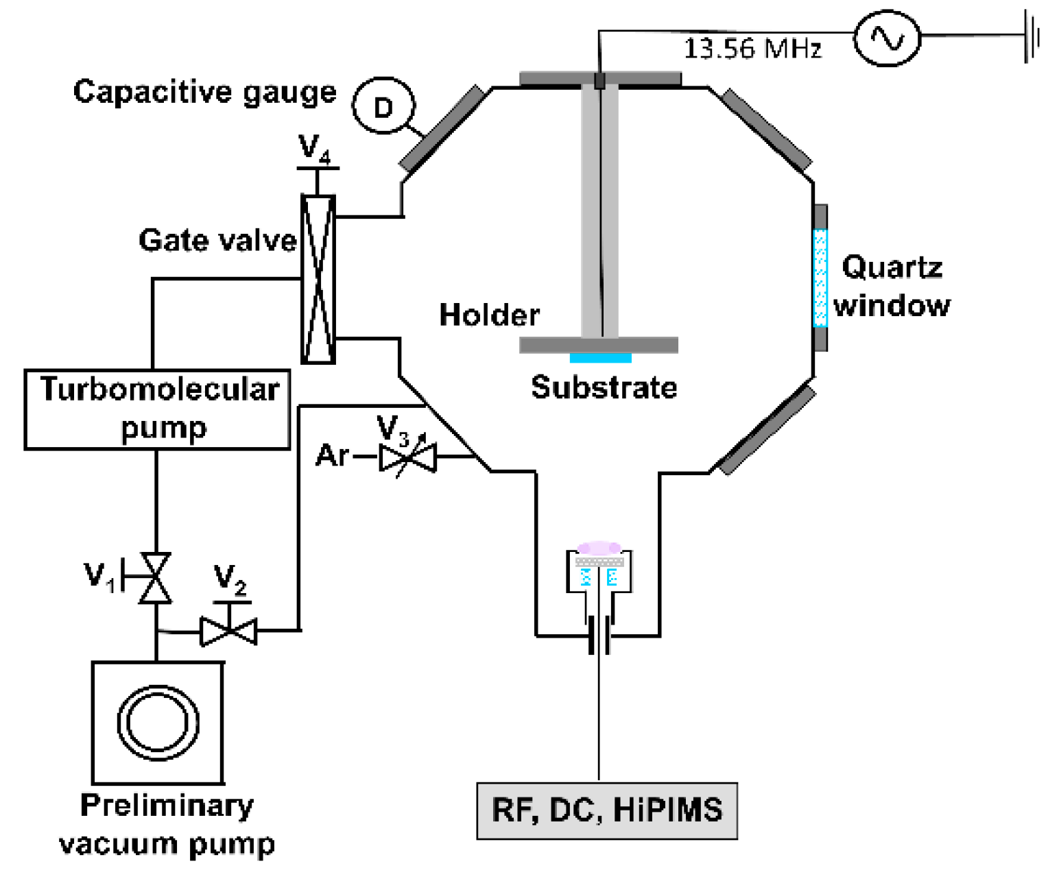
The copper and SiNx layers were obtained using a magnetron sputtering deposition system (Figure 1). The cathode (Φ = 50.8 mm) was alternatively equipped with pure Cu and Si targets (99.99 % purity, 6.35 mm thickness, Kurt J. Lesker Co., Hastings, UK) fed by DC, HiPIMS, and RF generators, respectively. The distance between the target and substrate was 9 cm, while the working pressure was kept constant by an automatic valve at 5 mTorr during all deposition runs. The metallic and dielectric films were grown on both Si (111) (Si-Mat Silicon Materials Co., Kaufering, Germany) and glass substrates with thicknesses of 0.5 mm and 1 mm, respectively. Two types of magnetron sputtering processes were used to deposit copper thin films: DCMS (Direct Current Magnetron Sputtering) and HiPIMS (High-Power Impulse Magnetron Sputtering).

Figure 1.
Experimental set-up of the magnetron sputtering deposition system.
For DCMS discharge, the copper target was powered by a DC generator, working in constant power mode (P = 10 W) corresponding to a current of 38 mA. The use of a low-power mode was necessary to allow for the deposition of very thin films, as needed in these types of applications. A pre-ionization source was used in the case of the HiPIMS process in order to ensure a constant DC current of 4 mA, overlapping the power pulses with a duration of 50 µs and a corresponding voltage of 600 V. Therefore, the chosen pulse repetition frequency was established at 25 Hz, leading to an average power of approximately 11 W, which is comparable to that used in DCMS. The substrates were negatively biased using an RF generator, and the value of DC self-bias voltage to the substrates was used as a control parameter to achieve a large tunability of the envisage layer’s properties. During the deposition process, three bias voltages of 0, −50 V, and −100 V were used. The SiNx layers with different Si/N concentrations were obtained by using a RFMS (Radiofrequency Magnetron Sputtering) discharge in a constant power regime at 90 W power input. A pure silicon target (99.99 purity, Φ = 50.8 mm, 6.35 mm thickness) was sputtered in a reactive gas mixture of Ar and N2 with different concentrations. The following ratios between Ar and N2 gas flows were used: 7/3 and 9.25/0.75, respectively.
The transmission and reflectivity measurements were assessed by UV-Vis-NIR spectrophotometry measurements (Jasco, Tokyo, Japan). In 250–2000 nm spectral range. The Jasco V-670 spectrophotometer (Jasco, Tokyo, Japan) was equipped with an ARSN 733 auxiliary unit that includes a 60 mm integrating sphere. The optical arrangement of the ARSN 733 unit allows obtaining both the absolute reflectance and transmission on the same film’s spot covering the transparent glass substrates. All measurements were carried out at a 5° angle incidence with respect to the normal incidence of light and a scan speed of 400 nm/min. The optical properties of all films were derived by using a commercial OptiLayer thin film software v15.12 (OptiLayer GmbH, Garching bei Munchen, Germany) [21,22,23]. The optical modeling of the multilayer structure of the type D/M/D, where the dielectric D is SiNx and the metal M is Cu, was also performed using OptiLayer software. The thicknesses were attained by profilometry measurements after removing the mask that covered the Si(111) substrates during the sputtering process. A Dektak profilometer (Veeco Instruments, Plainview, NY, USA) equipped with a tip of 2.5 µm curvature radius was used to ensure a complete scan of substrate–layer ensemble. The surface topography of thin films was investigated by using the atomic force microscopy (AFM) (Veeco Instruments, Plainview, NY, USA). The topography was evaluated by using an AFM Microscopy System (INNOVA Veeco, Berlin, Germany) running in the tapping mode at room temperature in ambient air. The AFM images were acquired on a surface area of 5 × 5 µm2 in order to determine the average roughness parameter by using the SPM Lab Analysis software. The phase composition of the samples was investigated by X-ray diffraction (XRD) using a SmartLab diffractometer (Rigaku, Tokyo, Japan) with CuKα radiation (λ = 1.540597 Å). The measurements were performed in a 2theta range from 40° to 55°, and the data were recorded with 1°/min. The grain sizes for the investigated samples were calculated from the XRD patterns using Scherrer’s equation.
3. Results and Discussion
All the deposition runs were performed on transparent microscope glass substrates in order to ensure the optical characterization phase of each type of layer. In the case of metallic layers that are to fulfill the function of a reflector in the NIR spectral range, both initial ex situ properties and their performance over time are essential. Due to long-term exposure to external factors such as atmospheric air, humidity, temperature, etc., the initial properties can be significantly affected. This damage is all the more important, as the layer is longer exposed by the formation of compounds that can totally or partially affect the properties of the metallic layer.
3.1. Optical Properties of Monolayers Obtained by DCMS, HiPIMS, and RF Techniques
3.1.1. Copper Metallic Layers
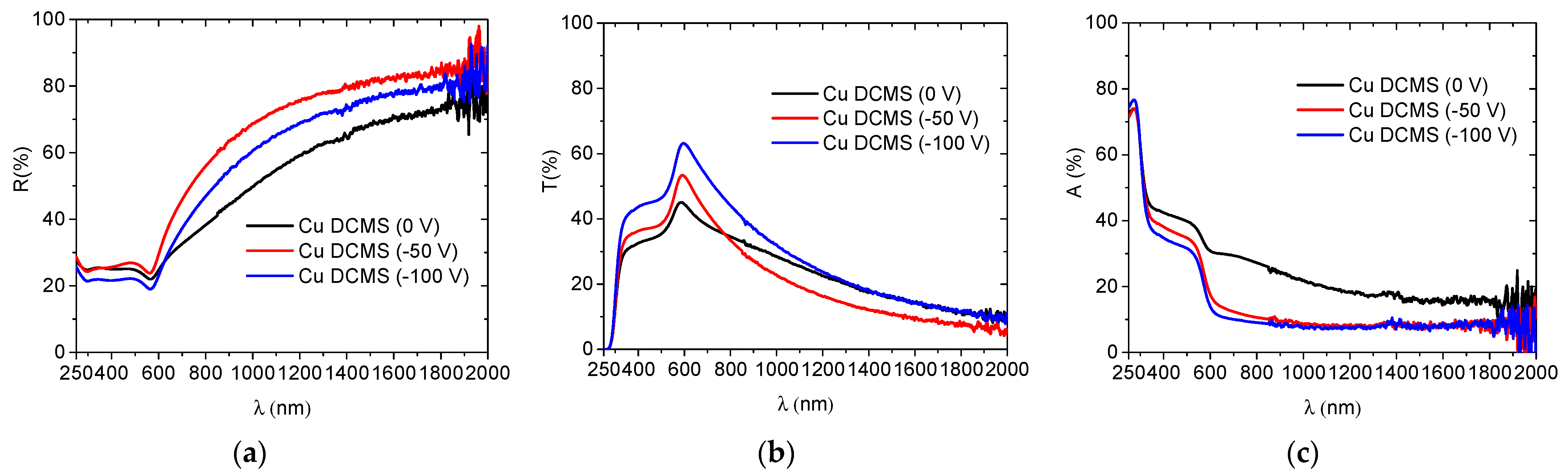
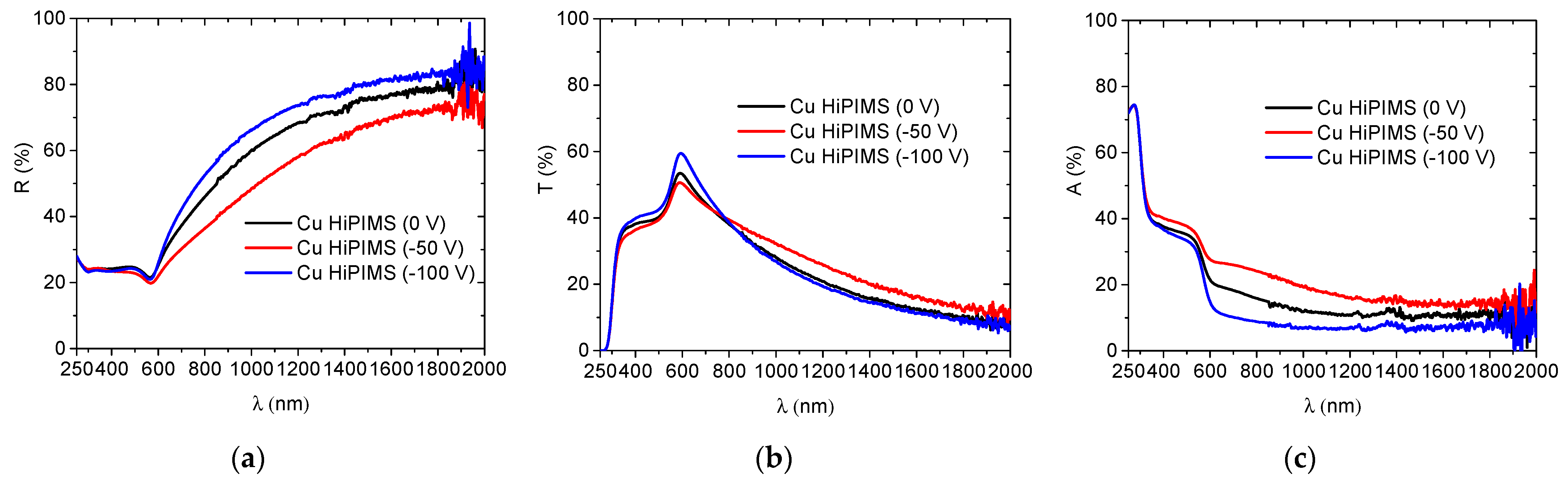
The initial reflection, transmission, and absorption curves for three layers obtained in DC and HiPIMS sputtering mode are shown in Figure 2 and Figure 3. These spectra were obtained practically immediately after removing them from the deposition system and should reflect the maximum ideal performances of the layers. It can be seen that there is an optimum in terms of reflectivity, its maximum being reached at a polarization voltage of the substrate of −50 V. However, in terms of transmission, the optimum is obtained for a polarization voltage of −100 V, with a maximum transmission that reaches 60%. This can be attributed to a relative thickness decrease in the film, considering that at −100 V bias voltage, some possible re-sputtering effects might occur.

Figure 2.
Comparison between reflectivity (a), transmission (b), and absorption (c) spectra of copper thin films obtained by using DCMS techniques at different substrate bias voltages.

Figure 3.
Comparison between reflectivity (a), transmission (b), and absorption (c) spectra of copper thin films obtained by using HiPIMS techniques at different substrate bias voltages.
The layer obtained without using a bias voltage (0 V) is the least interesting from the application point of view, having a reflectivity that reaches only ≈65% in the IR spectral range and has an important absorption over the entire spectral range.
For the HiPIMS obtained samples, on the other hand, an optimum can be observed for the −100 V biased sample (Figure 3). For these conditions, a maximum reflectivity in the IR range is reached, around 80%, the absorption values being negligeable starting from the middle of the visible spectral range and continuing in NIR intervals. It follows that these experimental conditions, with the highest ion flux available and their highest energy, are best suited for obtaining metallic layers that combine strong IR reflection and high transmission in the visible range. This optical behavior can be certainly ascribed to a superior density of the layers obtained in the HiPIMS regime at −100 V substrate polarization voltage.
The most unfavorable conditions are found for a −50 V bias value, with small values of reflectivity in the IR and high absorption. This is in line with the results obtained in [7], suggesting that there is a difference in the flux composition arriving at substrate in the 0 to −50 V interval, as compared with the −50 to −100 V interval. Indeed, when the substrate is not biased, Ubias = 0 V, there is an important flux of electrons in during the pulse ignition and first stages of the pulse [24]. When increasing the bias voltage, the electron flux is diminishing and the ion flux is increasing, up to a certain saturation value [25]. This corresponds roughly to the −50 V bias conditions, depending on the pressure and substrate position. Further increasing of the bias voltage leads to an increase in the energy of ions, keeping their flux roughly constant. Therefore, the −100 V conditions has an extra energy delivered to the substrate through the difference in bias voltage, −50 to −100 V. By comparison, when increasing the voltage from 0 to −50 V, the changes in the composition of the flux from dominantly electrons to predominantly ions lead to a much smaller effect on the energy balance.
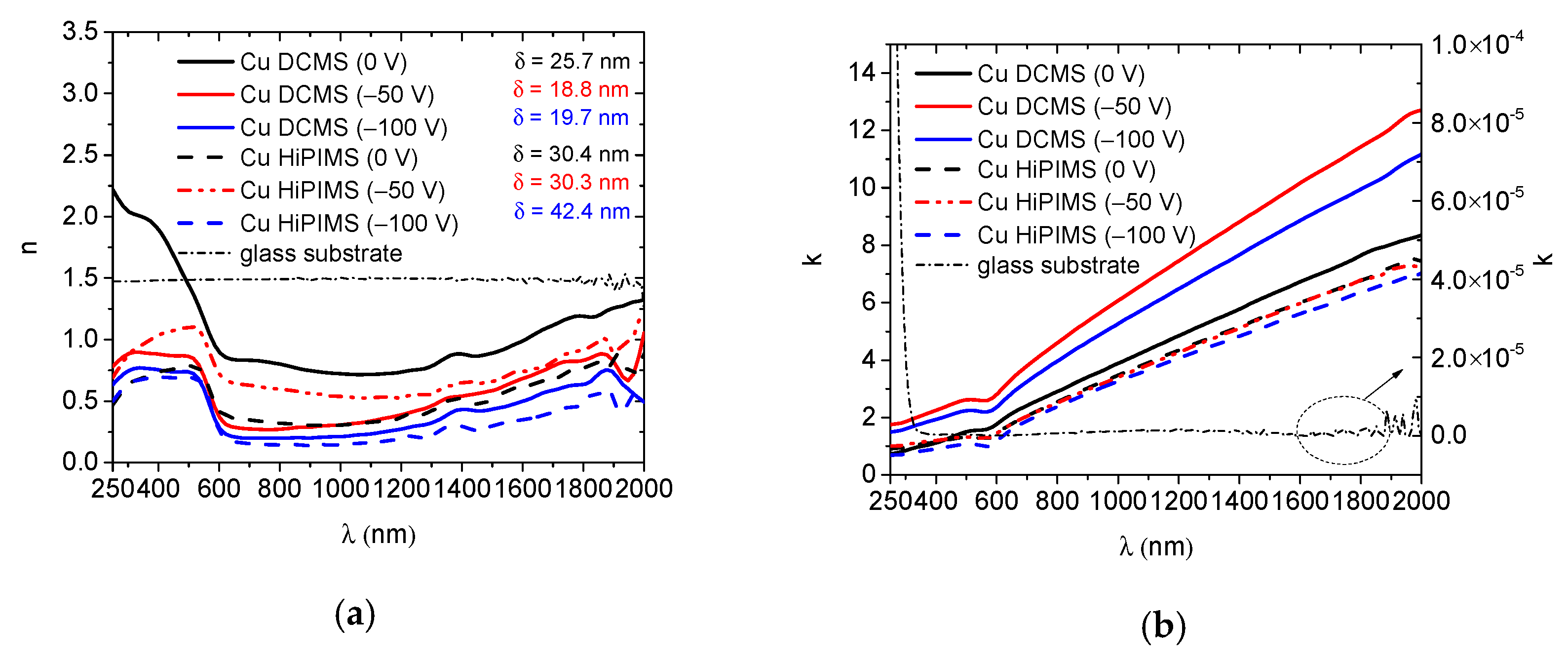
The spectrophotometric data from Figure 2 and Figure 3 served as input for the consequent modeling and optimization procedures. The refractive index n and the extinction coefficient k were derived as well as the thicknesses (δ) of all investigated layers. The thickness values were similar to the ones determined by profilometry measurements, confirming the results obtained from optical characterization (OptiChar module of OptiLayer). Figure 4 shows the dispersion curves of n and k for Cu layers obtained in DCMS an HiPIMS, at different bias voltages. An important variation of the refractive index can be observed, highlighting a clear dependence of the layer’s optical properties on the deposition conditions. Mostly all refractive indices values are situated below the one corresponding to the glass substrate, this being a common feature of metallic layers [26]. The extinction coefficient values are several orders of magnitude higher than the glass substrate. In addition, a higher extinction coefficient is revealed for the samples deposited by DCMS, making them unsuitable for glazing application. Indeed, the degradation caused by overheating phenomena can change drastically the absorption coefficient, which can contribute to excessive absorption and additional heating. Even if the surface profilometry measurements were performed on samples immediately after the deposition process, the obtained values (Figure 4) from copper films deposited on silicon substrates were used only as a reference for further determination of optical constants dispersion. In addition, the thickness values obtained by using advanced non-parametric models on coatings deposited on glass substrates were in good agreement with the ones obtained by surface profilometry. In the case of all DCMS copper samples, the deposition time was 5 min, while in the case of the HiPIMS process, the deposition time was 4 min. The surface inhomogeneities in the copper thin films were taken into account by searching for typical inhomogeneities near the substrate and ambient boundaries. The obtained results after the optical fitting procedure indicated the presence of thin overlayers with thicknesses around 0.5 nm or even smaller.

Figure 4.
Refractive indices (a) and extinction coefficients (b) of copper films in DCMS and HiPIMS mode derived from transmission and reflectance spectra.
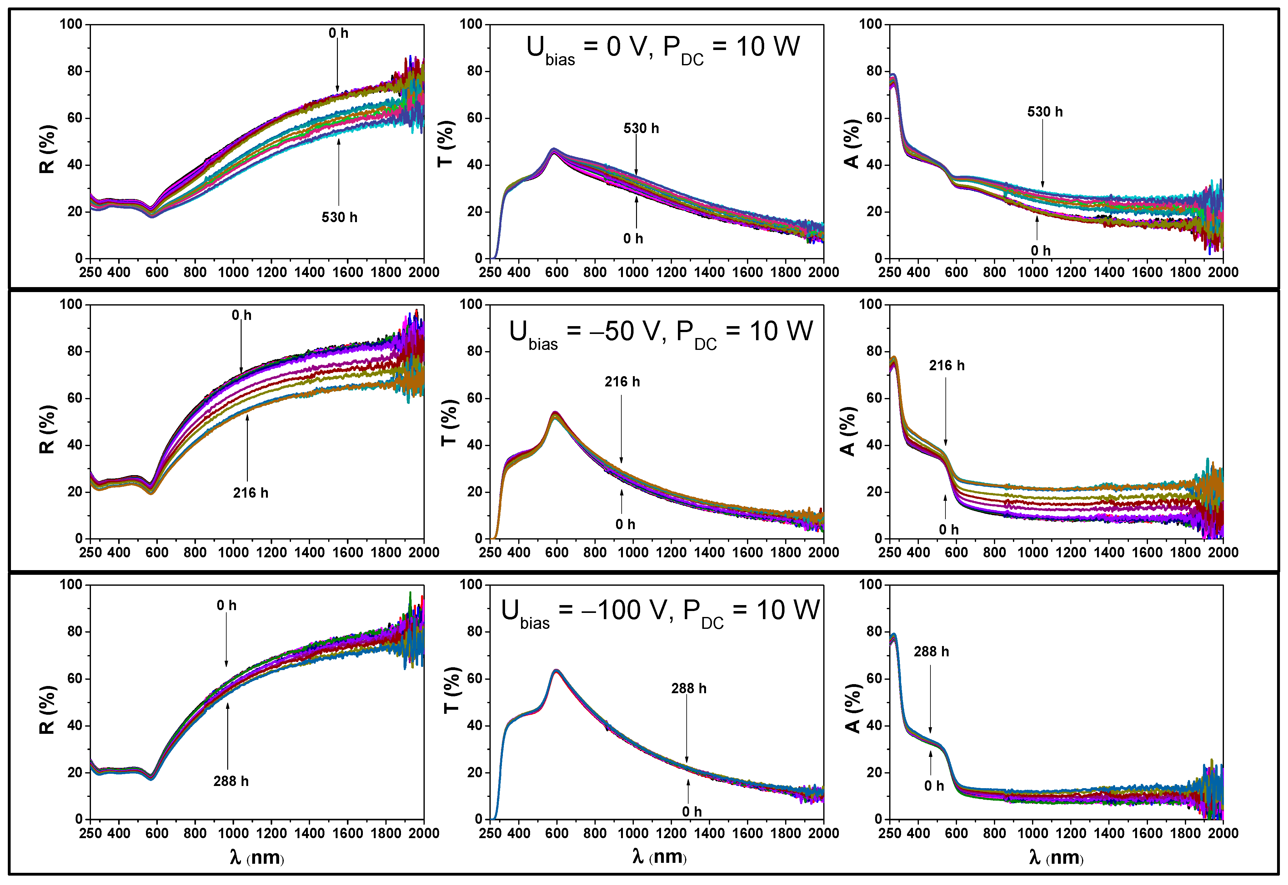
Figure 5 shows the evolution over time of reflectivity, transmission, and absorption values for the three types of layers obtained in DCMS mode. The spectral curves obtained immediately after removing the samples from the deposition chamber, also shown in Figure 2, are identified by “0 h”, while the last recorded curve is marked with the corresponding number of hours elapsed since the first measurement. The curves were recorded at intervals of several hours in the first 24 h after deposition, after which they were recorded at an interval of approximately 24 h. Several important aspects can be highlighted from this analysis on the temporal evolution of these spectral curves.

Figure 5.
Experimental transmission, reflectance and absorption spectra of copper films obtained immediately after DCMS deposition process (0 h) and after several days exposure to atmospheric pressure conditions.
As can be seen, the optical properties are changing from the very first hours after the samples are taken out into the ambient air due to the oxidation phenomena, which occurs at the sample’s surface [12]. If the metal layer is not protected by a dielectric layer, the optical characterization should be performed immediately after transition from vacuum to the atmospheric pressure conditions. In this way, a more accurate evaluation of its optical properties by spectrophotometry measurements is ensured. One should note that during atmospheric exposure, the optical properties evolve in the same direction: the decrease of the reflectivity in the IR range, the increase of the transmission in the visible spectral range, and the increase of the absorbance on the whole spectral range.
Thus, for the layers obtained using a bias voltage of 0 and −50 V, respectively, there is an important variation of all properties, while the layer obtained using a bias voltage of −100 V is the least sensitive to prolonged exposure to the atmosphere.
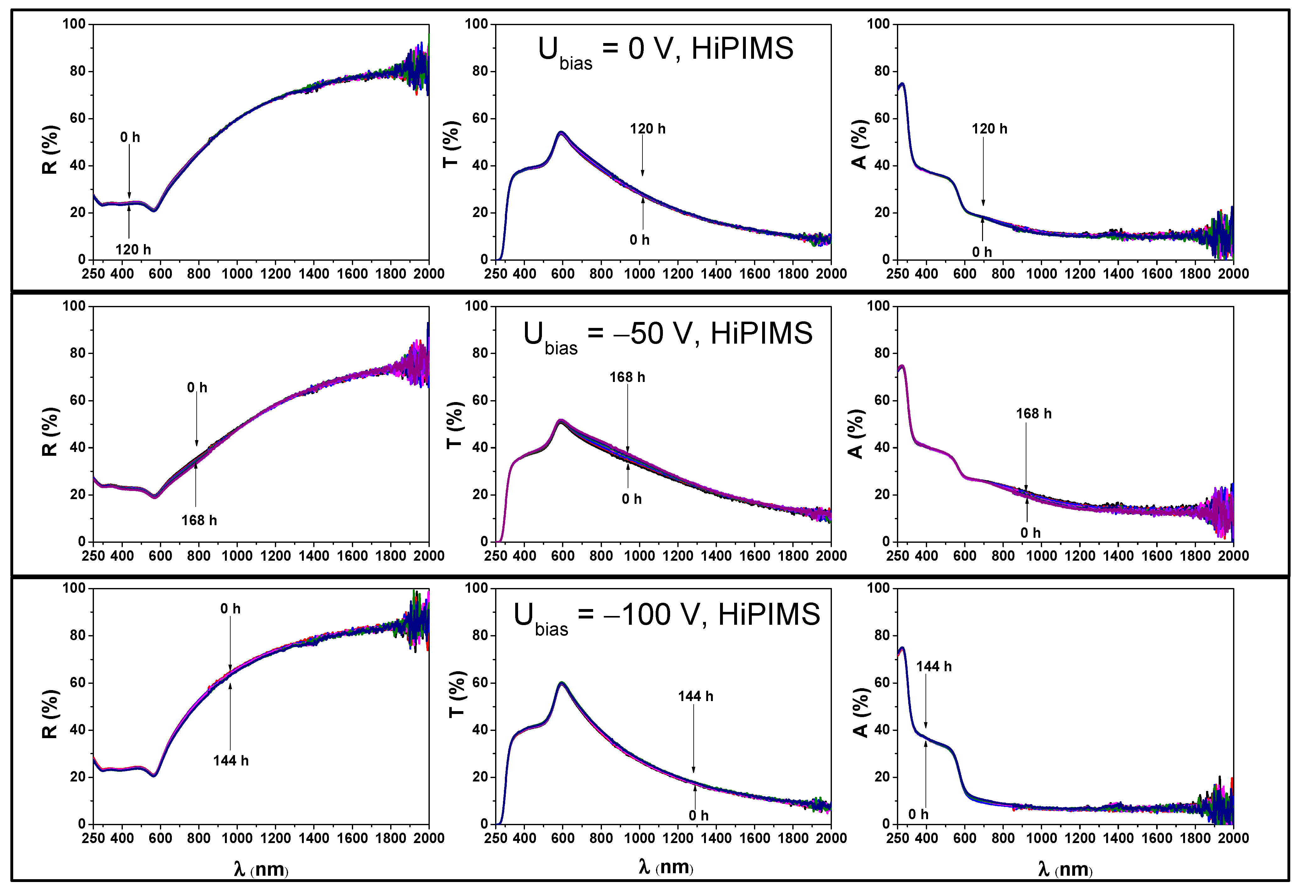
From the analysis of the evolution over time of the spectral curves obtained in the HiPIMS process (Figure 6), one can observe a much higher stability for all samples as compared to layers deposited in DCMS at the same bias voltages. Basically, the values remain almost unchanged, being closer to the equipment accuracy limit of ±1%. Combining this information with the fact that the initial properties are better for the layer obtained at −100 V bias voltage from the beginning, it becomes obvious that these are the process conditions that are suitable for a transparent heat reflector application, respectively, an HiPIMS sputtering and a polarization of the substrate at −100 V. These coatings have the potential to be much more stable over time, less sensitive to long-term exposure to environmental factors, and independent of the protection offered by the dielectric layer.

Figure 6.
Experimental transmission, reflectance, and absorption spectra of copper films obtained immediately after the HiPIMS deposition process (0 h) and after several days exposure to atmospheric pressure conditions.
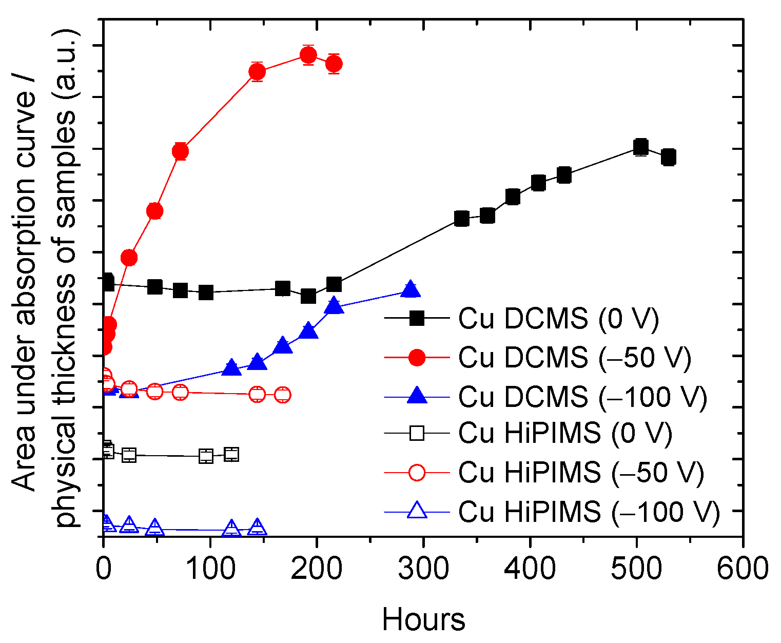
In order to have a general view on the temporal behavior for all conditions, both DC and HiPIMS, the area under the absorption curve, normalized to the thickness, is represented in Figure 7. It can be seen from the start that the HiPIMS films have a better quality as compared to the DC ones, having generally lower absorption values. The time evolution of the absorption, on the other hand, shows a clear increase for all DC deposited thin films, whereas the HiPIMS deposited ones show constant values over time. The optimum condition resulting from this time dependency is confirmed to be the HIPIMS deposition at −100 V, with the lowest absorption of all and highest stability over time. The DC deposited sample at −50 V, on the other hand, shows the sharpest increase in time, suggesting a fast degradation of the optical properties.

Figure 7.
Quantitative evaluation of absorption spectra as a function of time evolution for all copper films.
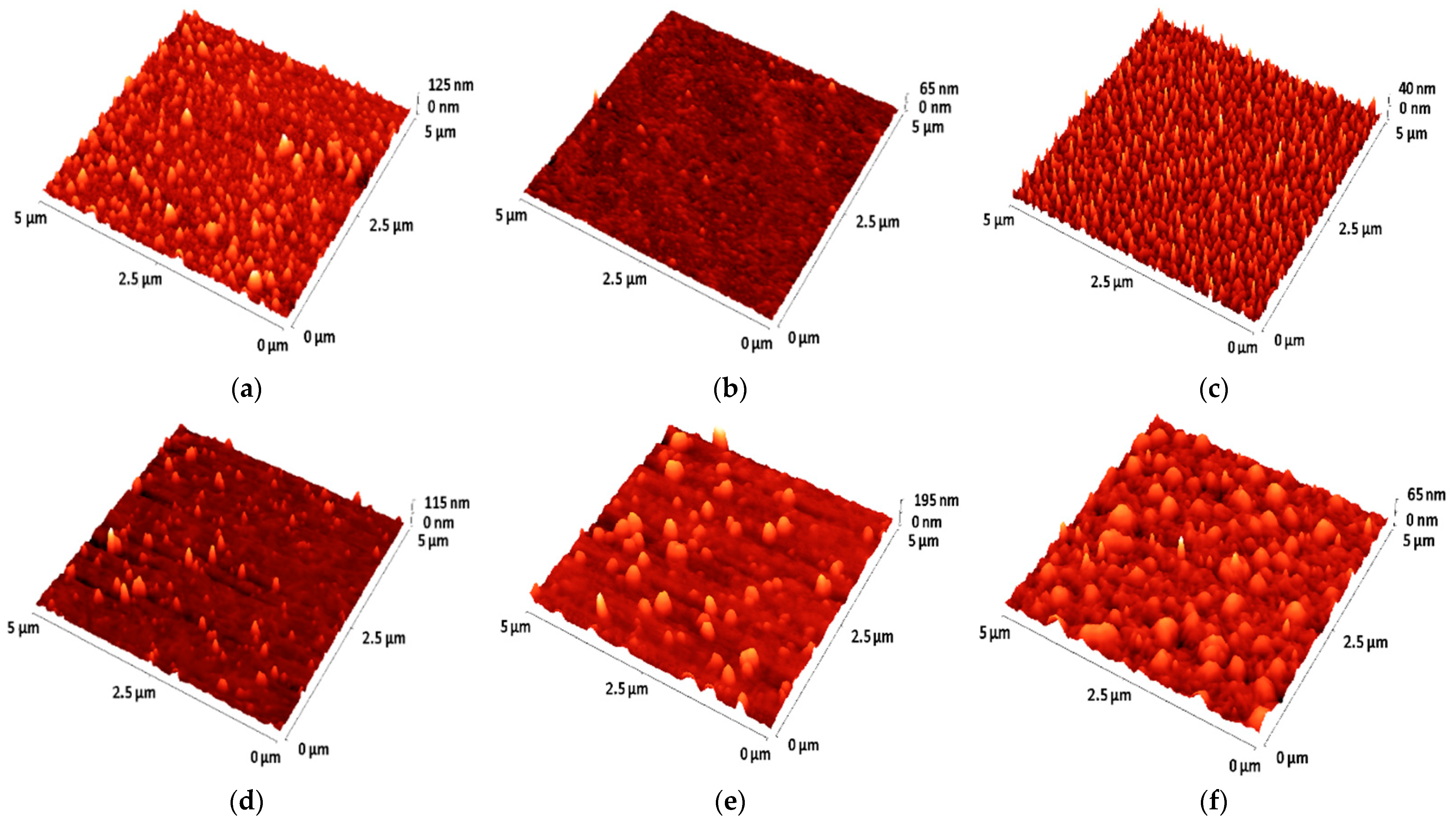
In order to check the long-term stability of the samples, their surfaces were investigated by atomic force microscopy. The AFM images of the samples deposited on the Si substrate under HiPIMS and DC conditions and exposed to air for 12 months are presented in Figure 8. Before acquiring the AFM images, the samples were cleaned under nitrogen flow to remove any residues from the surface. The images of the samples on the top side of the Figure 8 correspond to the HiPIMS samples, whereas the ones on the bottom side correspond to DC sputtering conditions.

Figure 8.
AFM images of Cu films obtained by HIPIMS at different bias voltages: (a) −0 V, (b) −50 V, (c) −100 V, and by DC sputtering: (d) −0 V, (e) −50 V, (f) −100 V.
The images are arranged from left to right, corresponding to bias voltages of 0 V (left), −50 V (center), and −100 V (right). The surface of the sample obtained in HiPIMS conditions appears as the most uniform, without significant features on the surface and an average roughness Ra = 3.4 nm. When decreasing the bias voltage, the number of features on the surface increases, indicating inhomogeneities and possible degradation of the surface. The surface of the sample obtained at −50 V bias voltage is the smoothest of all, with an average roughness Ra = 2.23 nm. For the samples obtained by DC sputtering, the situation is quite opposite, the number of defects and their size increase when increasing the voltage. The surface roughness is 3.62 nm for the sample obtained without bias and 5.19 nm for the sample obtained at −100 V bias voltage. The highest roughness was measured for the sample obtained at −50 V bias voltage. Let us not forget that for these conditions, the variation of optical properties in the first days after exposure was the highest, as seen in Figure 5. This confirms the initial trend of accelerated degradation observed for these experimental conditions.
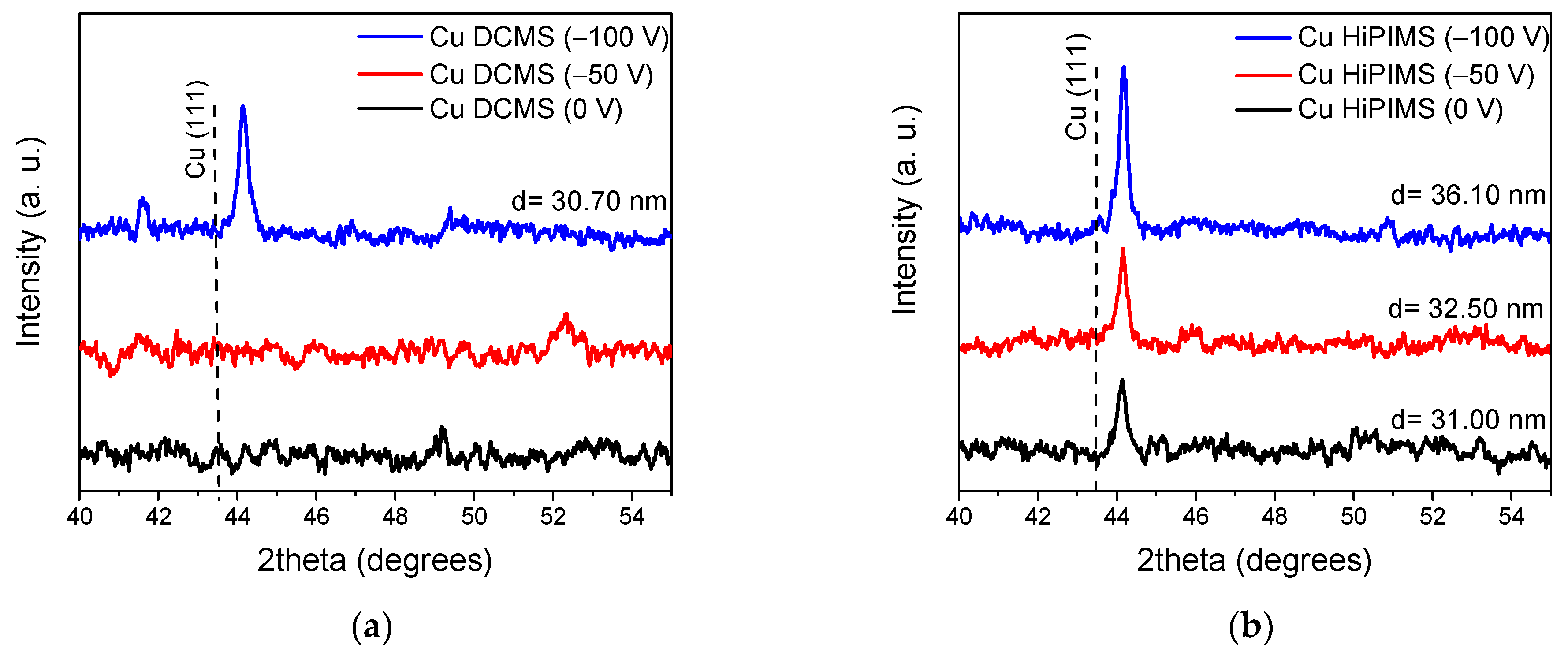
The samples deposited on glass substrate and exposed to air for 12 months were investigated by X-ray diffraction (XRD), using a SmartLab diffractometer (Rigaku, Tokyo, Japan) with CuKα radiation (λ = 1.540597 Å). The phase composition of copper thin films (glass substrate) obtained by using DCMS and HiPIMS techniques is presented in Figure 9. In the DCMS condition, for a grounded substrate (0 V Bias) and also when applying a low bias voltage (−50 V), an amorphous structure was observed, as indicated by the corresponding XRD patterns. A further increase in the negative bias voltage up to −100 V resulted in the appearance of the main 111 reflection of Cu with a cubic structure (according to JCPDS 4-009-2090) at 44.11°.

Figure 9.
XRD patterns of copper thin films obtained by using DCMS (a) and HiPIMS (b) techniques at different substrate bias voltages.
However, there is a peak shift in the measured patterns as compared with the peak position in the mentioned standard, which can be caused by a decrease in lattice parameters and cell refinement due to copper partial oxidation. For the samples obtained using the HiPIMS technique, the peak with 111 preferred orientation was present in all the investigated patterns regardless of the applied bias. The results also indicated an enhancement of peak crystallinity depending on the negative substrate bias. The calculated grain sizes increased from d = 31 nm in the case of grounded substrate to d ≈ 36 nm for the highest bias voltage applied (−100 V). It results then that better crystallinity of the films is associated to higher stability to oxidation, the most stable optical conditions, Figure 5 and Figure 6, being observed for the samples that keep a good crystallinity even after 12 months of storage in ambient air.
3.1.2. SiNx Dielectric Layers
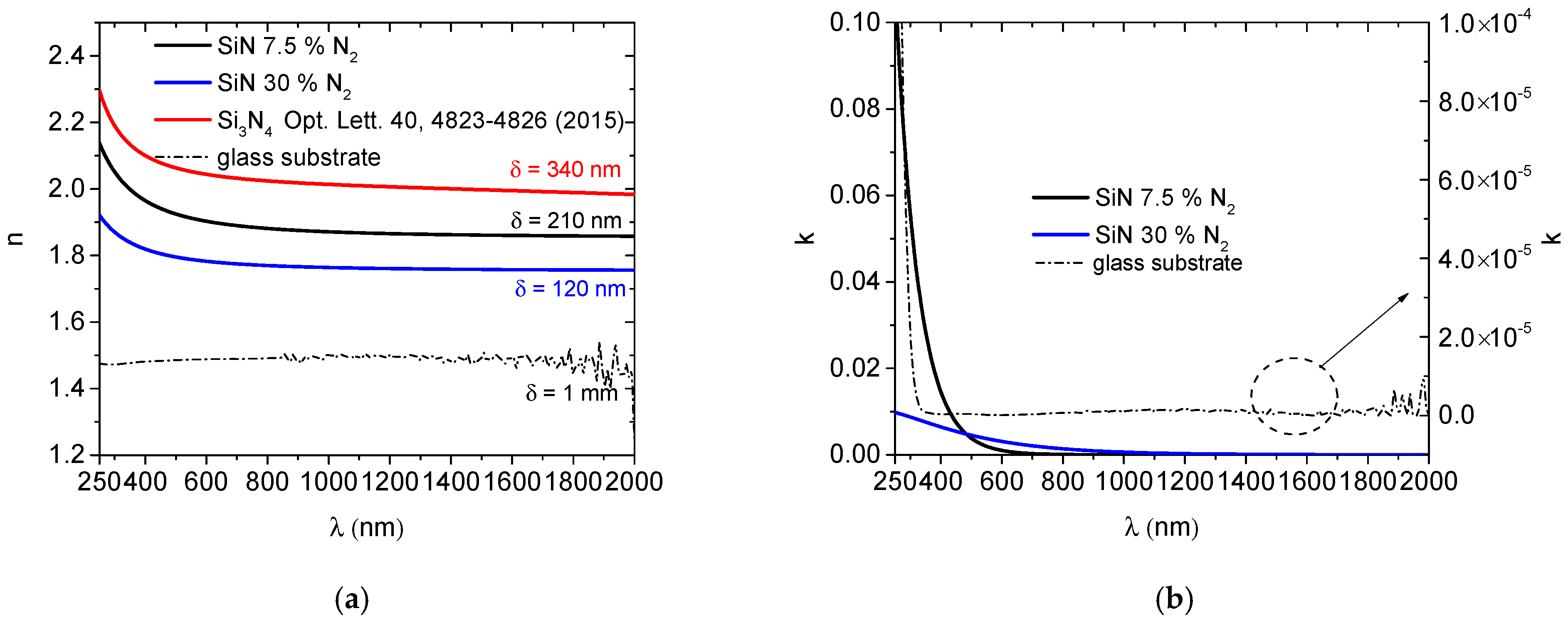
The SiNx optical properties are highly dependent on the deposition conditions. In order to evaluate the potential of copper-based theoretical multilayer structures with THR properties, three types of layers were chosen as representative for very different optical properties achievable with SiNx thin films. Two of them were obtained experimentally in very different reactive conditions, namely low nitrogen content corresponding to 7.5% of N2 flow from the total and 30% of N2 flow from the total [27]. The third condition corresponds to an almost ideal condition from the literature [28] to be compared with the experimental ones. The optical constants for these three types of thin films are represented in Figure 10, showing an interval of variation for the refractive index from 1.8 to 2.0. The extinction coefficient for the experimental SiNx films is represented in Figure 10b, and the extinction coefficient of the ideal Si3N4 material is considered to be zero in the following.

Figure 10.
Experimental n (a) and k (b) parameters for SiNx layers for three different conditions.
3.1.3. Optical Modeling of THR Structures
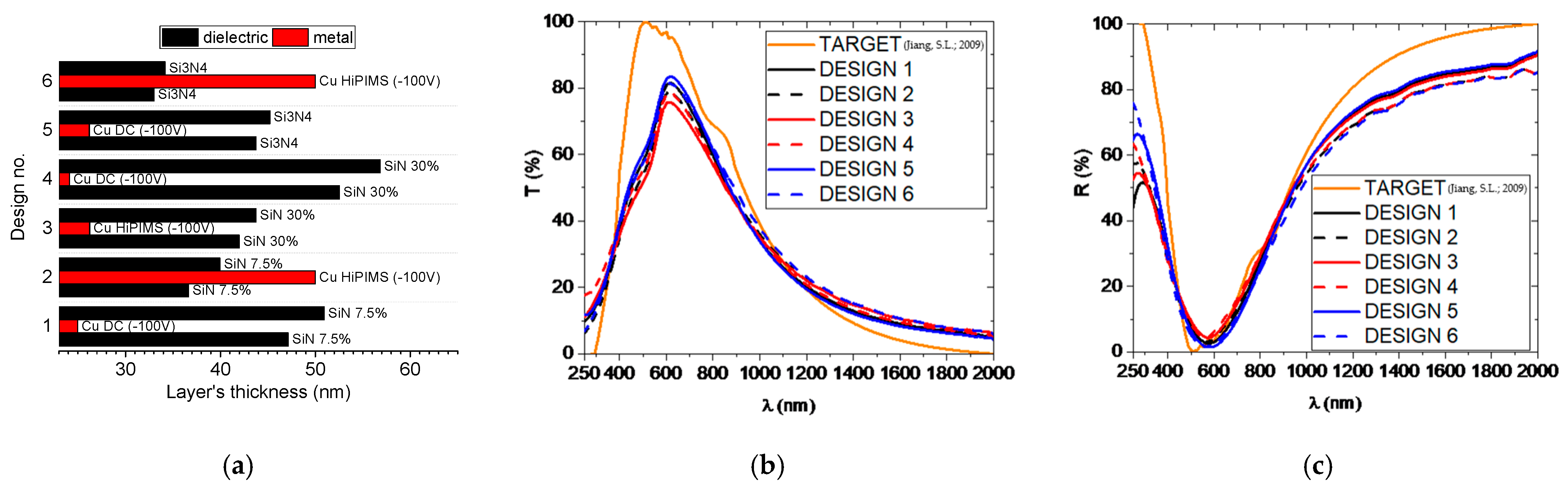
The optical modeling of the THR structure was performed using the OptiLayer software. The targeted reflection and absorption follow the terrestrial solar spectral irradiance (AM1.5G) [29] and are represented in Figure 11. For the modeling of the multilayer structure, two types of Cu layers were used, namely the one obtained in DC and HiPIMS with −100 V bias voltage. Considering both their initial properties, the lowest refractive indices from the series, and their stability over time, as shown in Figure 7, these are the conditions with the highest potential for the application. For the dielectric layer, the three types of SiNx previously described were taken into account, using the optical properties represented in Figure 8. By combining these two types of Cu thin films with the three types of SiNx it results in six possible combinations of multilayers having the structure SiNx/Cu/SiNx (Figure 11a).

Figure 11.
Theoretical designs (a) characterized by specific T (b) and R (c) spectra for different dielectric–metal combinations [29].
Several individual layer thickness constraints were imposed in the design approach process as for each type of layer, metal or dielectric. In the case of metallic layers, the thicknesses interval varied from 10 nm up to 50 nm, while the thickness of dielectric layers was allowed to vary in the 10–60 nm interval. The lower and upper thickness limits for metallic layers were chosen in order to avoid having thicknesses smaller than a few atomic layers that will be practically impossible to be experimentally obtained by PVD processes. The SiNx limits were established to obtain a three-layered structure with a total thickness smaller than 200 nm. The targeted transmittance and reflectance were defined by considering a 1 nm step in the 250–2000 nm spectral range. For all considered designs, the optical properties of the glass substrate were the ones depicted in Figure 4a,b, while the refractive index of the incident medium (air) was set to be 1 (k = 0). In order to obtain a minimum value of the design’s merit function during the gradual evolution of the needle-optimization technique, 1% tolerances were assumed.
The optimized spectrophotometric curves calculated for these combinations are represented in Figure 11b,c and compared with the initial target. It results that by optimizing each of the designs, similar properties can be obtained from these six versions of the multilayer. A slightly higher transmission in the visible range could be obtained for the DC thin film at −100 V bias combined with the ideal Si3N4 thin film.
As a general remark, the best properties are obtained when using the stoichiometric Si3N4, so the quality of the dielectric layer is important when optimizing the structure. The DC copper films seem to perform slightly better, with merit functions that are typically lower than the ones for the HiPIMS films. Nevertheless, their instability over time would make them challenging to be used in real life due to the changes of their optical properties.
4. Conclusions
SiNx and copper films were obtained by using the magnetron sputtering technique including RFMS, DCMS, and HiPIMS. The experimental conditions were established in order to a have a good reproducibility and to ensure a minimum layer’s thickness for preserving the optical properties. The optical parameters of the films were assessed by using spectrophotometry measurements in conjunction with an advanced optical characterization. All the investigated SiNx and copper films have presented a good tailorabillity in terms of refractive index and extinction coefficient. The copper films obtained by the HiPIMS processes proved to be more stable over time than the ones obtained by DCMS. In addition, this aspect implies a better protection against oxidation by coating itself after a long-term utilization period under atmospheric pressure conditions and in a dielectric-metal–dielectric structure. In this way, it might ensure both a stable optical behavior over time and an enhanced mechanical response. According to the envisaged application, the coatings proved to be suitable for theoretical multilayer designs, possessing a low reflectivity in the visible range along with a high reflectivity in the near infrared spectral range.
Author Contributions
Conceptualization, C.V.; Data curation, A.C.P. and I.P.; Formal analysis, A.E.K. and L.R.C.; Investigation, A.C.P., I.P. and M.D.; Methodology, A.E.K. and L.R.C.; Resources, L.R.C.; Software, I.P.; Supervision, C.V.; Validation, M.D. and A.E.K.; Writing—original draft, I.P. and C.V.; Writing—review and editing, I.P. and C.V. All authors have read and agreed to the published version of the manuscript.
Funding
This work was funded by the Romanian Ministry of Education and Research, CCCDI—UEFISCDI, project numbers PN-III-P1-1.1-TE-2019-1924 TE 105, and PN-III-P2-2.1-PED-2019-4966 PED 489, within PNCDI III.
Institutional Review Board Statement
Not applicable.
Informed Consent Statement
Not applicable.
Data Availability Statement
Not applicable.
Acknowledgments
The authors also want to thank the Core Program, Project No. 18N/2019.
Conflicts of Interest
The authors declare no conflict of interest. The funders had no role in the design of the study; in the collection, analyses, or interpretation of data; in the writing of the manuscript, or in the decision to publish the results.
References
- Blok, K.; Afanador, A.; Van Der Hoorn, I.; Berg, T.; Edelenbosch, O.Y.; Van Vuuren, D.P. Assessment of sectoral greenhouse gas emission reduction potentials for 2030. Energies 2020, 13, 943. [Google Scholar] [CrossRef] [Green Version]
- Rezaei, S.D.; Shannigrahi, S.; Ramakrishna, S. A review of conventional, advanced, and smart glazing technologies and materials for improving indoor environment. Sol. Energy Mater. Sol. Cells 2017, 159, 26–51. [Google Scholar] [CrossRef]
- Awad, M.A.; Raaif, M. Optical and electrical performance of transparent conductive TiO2/Cu/TiO2 multilayers prepared by magnetron sputtering. J. Mater. Sci. Mater. Electron. 2018, 29, 2815–2824. [Google Scholar] [CrossRef]
- Peng, L.; Jiang, S.; Guo, R.; Xu, J.; Li, X.; Miao, D.; Wang, Y.; Shang, S. IR protection property and color performance of TiO2/Cu/TiO2 coated polyester fabrics. J. Mater. Sci. Mater. Electron. 2018, 29, 16188–16198. [Google Scholar] [CrossRef]
- Dalapati, G.K.; Masudy-Panah, S.; Chua, S.T.; Sharma, M.; Wong, T.I.; Tan, H.R.; Chi, D. Color tunable low cost transparent heat reflector using copper and titanium oxide for energy saving application. Sci. Rep. 2016, 6, 20182. [Google Scholar] [CrossRef] [Green Version]
- Cemin, F.; Lundin, D.; Cammilleri, D.; Maroutian, T.; Lecoeur, P.; Minea, T. Low electrical resistivity in thin and ultrathin copper layers grown by high power impulse magnetron sputtering. J. Vac. Sci. Technol. A Vac. Surf. Film. 2016, 34, 051506. [Google Scholar] [CrossRef] [Green Version]
- Wu, B.H.; Wu, J.; Jiang, F.; Ma, D.L.; Chen, C.Z.; Sun, H.; Leng, Y.X.; Huang, N. Plasma characteristics and properties of Cu films prepared by high power pulsed magnetron sputtering. Vacuum 2017, 135, 93–100. [Google Scholar] [CrossRef]
- Tiron, V.; Velicu, I.L.; Vasilovici, O.; Popa, G. Optimization of deposition rate in HiPIMS by controlling the peak target current. J. Phys. D Appl. Phys. 2015, 48, 495204. [Google Scholar] [CrossRef]
- Helmersson, U.; Lattemann, M.; Bohlmark, J.; Ehiasarian, A.P.; Gudmundsson, J.T. Ionized physical vapor deposition (IPVD): A review of technology and applications. Thin Solid Film. 2006, 513, 1–24. [Google Scholar] [CrossRef] [Green Version]
- Velicu, I.-L.; Tiron, V.; Rusu, B.-G.; Popa, G. Copper thin films deposited under different power delivery modes and magnetron configurations: A comparative study. Surf. Coat. Technol. 2017, 327, 192–199. [Google Scholar] [CrossRef]
- Platzman, I.; Brener, R.; Haick, H.; Tannenbaum, R. Oxidation of polycrystalline copper thin films at ambient conditions. J. Phys. Chem. C 2008, 112, 1101–1108. [Google Scholar] [CrossRef]
- Iijima, J.; Lim, J.W.; Hong, S.H.; Suzuki, S.; Mimura, K.; Isshiki, M. Native oxidation of ultra high purity Cu bulk and thin films. Appl. Surf. Sci. 2006, 253, 2825–2829. [Google Scholar] [CrossRef]
- Ionescu, M.I.; Bensebaa, F.; Luan, B.L. Study of optical and electrical properties of ZnO/Cu/ZnO multilayers deposited on flexible substrate. Thin Solid Film. 2012, 525, 162–166. [Google Scholar] [CrossRef]
- Velicu, I.L.; Ianoş, G.T.; Porosnicu, C.; Mihăilă, I.; Burducea, I.; Velea, A.; Cristea, D.; Munteanu, D.; Tiron, V. Energy-enhanced deposition of copper thin films by bipolar high power impulse magnetron sputtering. Surf. Coat. Technol. 2019, 359, 97–107. [Google Scholar] [CrossRef]
- Viloan, R.P.B.; Helmersson, U.; Lundin, D. Copper thin films deposited using different ion acceleration strategies in HiPIMS. Surf. Coat. Technol. 2021, 422, 127487. [Google Scholar] [CrossRef]
- Roychowdhury, T.; Shah, D.; Jain, V.; Patel, D.I.; Dodson, B.; Skinner, W.; Hilfiker, J.N.; Smith, S.J.; Linford, M.R. Multi-instrument characterization of HiPIMS and DC magnetron sputtered tungsten and copper films. Surf. Interface Anal. 2020, 52, 433–441. [Google Scholar] [CrossRef]
- Szczyrbowski, J.; Bräuer, G.; Ruske, M.; Schilling, H.; Zmelty, A. New low emissivity coating based on TwinMag® sputtered TiO2 and Si3N4 layers. Thin Solid Film. 1999, 351, 254–259. [Google Scholar] [CrossRef]
- Hegedüs, N.; Balázsi, K.; Balázsi, C. Silicon nitride and hydrogenated silicon nitride thin films: A review of fabrication methods and applications. Materials 2021, 14, 5658. [Google Scholar] [CrossRef]
- Kouznetsov, V.; Macák, K.; Schneider, J.M.; Helmersson, U.; Petrov, I. A novel pulsed magnetron sputter technique utilizing very high target power densities. Surf. Coat. Technol. 1999, 122, 290–293. [Google Scholar] [CrossRef]
- Samuelsson, M.; Sarakinos, K.; Högberg, H.; Lewin, E.; Jansson, U.; Wälivaara, B.; Ljungcrantz, H.; Helmersson, U. Growth of Ti-C nanocomposite films by reactive high power impulse magnetron sputtering under industrial conditions. Surf. Coat. Technol. 2012, 206, 2396–2402. [Google Scholar] [CrossRef] [Green Version]
- Amotchkina, T.V.; Janicki, V.; Sancho-parramon, J.; Tikhonravov, A.V.; Trubetskov, M.K.; Zorc, H. General approach to reliable characterization of thin metal films. Appl. Opt. 2011, 50, 1453–1464. [Google Scholar] [CrossRef] [PubMed] [Green Version]
- Tikhonravov, A.V.; Trubetskov, M.K.; Kokarev, M.A.; Amotchkina, T.V.; Duparre, A.; Quesnel, E.; Ristau, D. Effect of systematic errors in spectral photometric data on the accuracy of determination of optical parameters of dielectric thin films. Appl. Opt. 2002, 41, 2555–2560. [Google Scholar] [CrossRef] [PubMed]
- Amotchkina, T.V.; Schlichting, S.; Ehlers, H.; Trubetskov, M.K.; Tikhonravov, A.V.; Ristau, D. Computational manufacturing as a key element in the design-production chain for modern multilayer coatings. Appl. Opt. 2012, 51, 7604–7615. [Google Scholar] [CrossRef] [PubMed]
- Poolcharuansin, P.; Bradley, J.W. Short- and long-term plasma phenomena in a HiPIMS discharge. Plasma Sources Sci. Technol. 2010, 19, 025010. [Google Scholar] [CrossRef]
- Oliveira, J.; Ferreira, F.; Serra, R.; Kubart, T.; Vitelaru, C.; Cavaleiro, A. Correlation between substrate ion fluxes and the properties of diamond-like carbon films deposited by deep oscillation magnetron sputtering in Ar and Ar + Ne plasmas. Coatings 2020, 10, 914. [Google Scholar] [CrossRef]
- Heavens, O.S.; Singer, S.F. Optical properties of thin solid films. Phys. Today 1956, 9, 24–26. [Google Scholar] [CrossRef]
- Pana, I.; Vitelaru, C.; Zoita, N.C.; Braic, M. Tunable optical properties of SiNx thin films by OES monitoring in a reactive RF magnetron plasma. Plasma Process. Polym. 2016, 13, 208–216. [Google Scholar] [CrossRef]
- Luke, K.; Okawachi, Y.; Lamont, M.R.E.; Gaeta, A.L.; Lipson, M. Broadband mid-infrared frequency comb generation in a Si3N4 microresonator. In Proceedings of the Conference on Lasers and Electro-Optics Europe—Technical Digest, San Jose, CA, USA, 10–15 May 2015; Volume 2015. [Google Scholar]
- Jiang, S.L.; Hu, P.; Mo, S.P.; Chen, Z.S. Modeling for two-stage dish concentrating spectral beam splitting photovoltaic/thermal system. In Proceedings of the Asia-Pacific Power Energy Engineering Confeference APPEEC, Wuhan, China, 28–31 March 2009; pp. 25–28. [Google Scholar] [CrossRef]
Publisher’s Note: MDPI stays neutral with regard to jurisdictional claims in published maps and institutional affiliations. |
© 2022 by the authors. Licensee MDPI, Basel, Switzerland. This article is an open access article distributed under the terms and conditions of the Creative Commons Attribution (CC BY) license (https://creativecommons.org/licenses/by/4.0/).