
A Review on Phase Field Modeling for Formation of η-Cu6Sn5 Intermetallic
by
 and
and
Jia Sun
1,
Lingyan Zhao
1,
Huaxin Liang
1,
Yao Zhang
2,
Xuexiong Li
3,
Chunyu Teng
4,
Hao Wang
2 and
Hailong Bai
1,* 1
R&D Center of Yunnan Tin Group (Holding) Co., Ltd., Kunming 650106, China
2
Interdisciplinary Centre for Additive Manufacturing (ICAM), School of Materials and Chemistry, University of Shanghai for Science and Technology, Shanghai 200093, China
3
Institute of Metal Research, Chinese Academic of Science, Shenyang 100016, China
4
AVIC China Aero-Poly Technology Establishment, Beijing 100028, China
*
Author to whom correspondence should be addressed.
Metals 2022, 12(12), 2043; https://doi.org/10.3390/met12122043
Submission received: 1 November 2022
/
Revised: 20 November 2022
/
Accepted: 23 November 2022
/
Published: 28 November 2022
(This article belongs to the Section Metal Casting, Forming and Heat Treatment)
Abstract
:Formation of intermetallic compounds (IMCs) exhibits remarkable microstructural features and provides opportunities for microstructure control of microelectronic interconnects. Excessive formation of brittle IMCs at the Cu/Sn interface such as η-Cu6Sn5 can deteriorate the reliability and in turn lead to solder joint failure in the Pb-free Sn-based solder joints. Phase field method is a versatile tool for prediction of the mesoscopic structure evolution in solders, which does not require tracking interfaces. The relationships between the microstructures, reliability and wettability were widely investigated, and several formation and growth mechanisms were also proposed for η-Cu6Sn5. In this paper, the current research works are reviewed and the prospective of the application of phase field method in the formation of η-Cu6Sn5 are discussed. Combined phase field simulations hold great promise in modeling the formation kinetics of IMCs with complex microstructural and chemical interactions.
1. Introduction
With the rapid miniaturization of electronic circuits, thermal, electrical, and mechanical loads on three-dimensional integrated circuits (3DIC) that provide the electrical connection between the substrate and the chip have increased [1,2,3,4]. During the soldering process, a layer of IMC is formed at the solder–substrate interface. On the one hand, a thin, continuous, and uniform IMC layer is an essential requirement for good bonding; on the other hand, since this IMC layer is quite brittle, it can adversely impact the mechanical properties of the joint [5]. In the subsequent aging process, the microstructure of the solder joint coarsens while the interface IMC layer thickens, resulting in stress concentration, promoting the nucleation and growth of cracks. Additionally, as the IMCs generally have lowered ductility and higher electrical resistivity than pure Sn or Cu, the larger proportion of interfacial IMCs at the solder–substrate interface is a major reliability concern [6]. Since one of the essential features of solder technology is the reaction of a molten solder with a conductive metal to form an IMC, striking characteristics of IMCs have attracted considerable interests. Recently, the phase field method has been used as a powerful computational tool for modeling and predicting morphological and microstructural evolution in solder materials [7,8,9,10].
Based on the formation stages of the IMCs, there are mainly two types of IMCs which form during the interfacial reactions on the Cu/Sn/Cu sandwich structure that have been discovered and investigated, η-Cu6Sn5 and ε-Cu3Sn. During the soldering process of Cu-Sn solder, the main reactions may happen as follows:
Figure 1 shows the schematic diagram of the solder wetting process and scanning electron microscope (SEM) morphology of Cu3Sn and Cu6Sn5 IMCs. Generally, the soldering process can be divided into three stages, as Figure 1a shows [11]: (a) spreading; (b) base metal dissolution; (c) formation of an IMC layer during which η-Cu6Sn5 and ε-Cu3Sn nucleate and grow at the solder/conductor interfaces successively. Both η-Cu6Sn5 and ε-Cu3Sn can form during the interface reactions in the Cu-Sn binary system. Reactions such as 5Cu3Sn→9Cu + Cu6Sn5 and 2Cu3Sn + 3Sn→Cu6Sn5 may also happen under different aging time and soldering conditions. The formation sequence of η-Cu6Sn5 and ε-Cu3Sn is still controversial at present since the experimental observations alone cannot give sufficient information to fully understand the growth kinetics and behavior of IMCs in solder joints [12,13,14,15,16].
η-Cu6Sn5 possesses a hexagonal structure (space group: P63/mmc) with and it maintains orientation relationships with the Cu pad according to the edge-to-edge matching model. The two best matching close-packed planes that contain the rows of atoms are and , as illustrated in Figure 2 [16]. Cu6Sn5 is scallop-type and forms very fast during soldering process. The high-temperature η-Cu6Sn5 is first formed during the soldering process, and when the temperature is below 186 °C, Cu6Sn5 phase will transform η into η′ (η′-Cu6Sn5), and the crystal structure will transform from hexagonal crystal to monoclinic crystal. The main object in this work is η-Cu6Sn5 that owns the hexagonal structure [5,14,15].
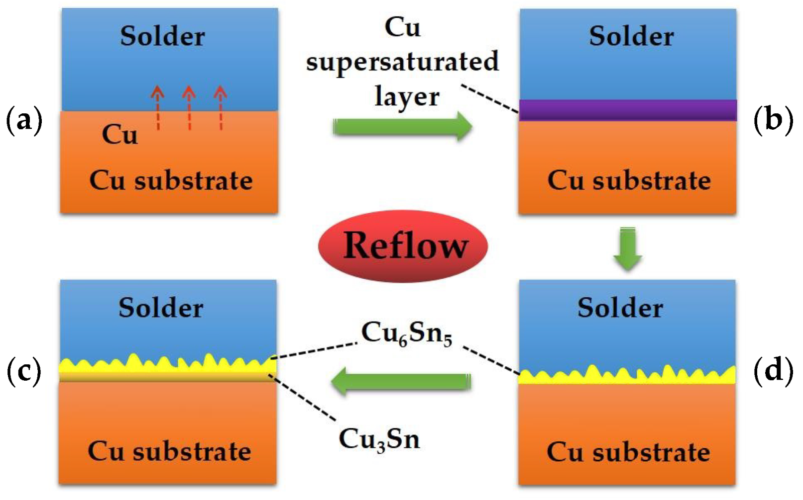
Cu3Sn forms between Cu6Sn5 and Cu if the contact of Cu substrates with the molten solder is long enough. In other words, Cu3Sn often nucleates and grows during the solder reflow process, as Figure 3 shows, and is also formed by diffusion and by reaction type growth as Cu6Sn5 [17]. Single crystalline Cu results in the growth of columnar Cu3Sn grains aligned in a thin uniform layer perpendicular to the interface, while a thick Cu3Sn layer formed from fine equiaxed grains on the polycrystalline substrate [18]. Cu3Sn or its interface with Cu (Cu3Sn/Cu) is prone to voiding, either by the Kirkendall effect or by solute segregation, and thus more generally investigated in regard to the formation and growth of micro-voids [10].
Compared to Cu3Sn, Cu6Sn5 is commonly the main research object due to its preferred formation, evident thickness, and thus greater effects on the microstructure and properties of solder joints [19,20]. Phase field simulations of IMCs’ growth in lead-free solder joints have been reported in the literature, including diffusion and mechanical deformation. The formation kinetics of IMCs are quite complex and there are still some aspects which need to be clarified. Furthermore, detailed research work needs to be carried out for practical applications. In this paper, the recent developments in the application of the phase-field method in IMCs are reviewed and future directions for the research are proposed.
2. Phase Field Method for Formation and Growth of IMCs
2.1. Free Energy Curves of Cu(S), Sn(L) and IMCs
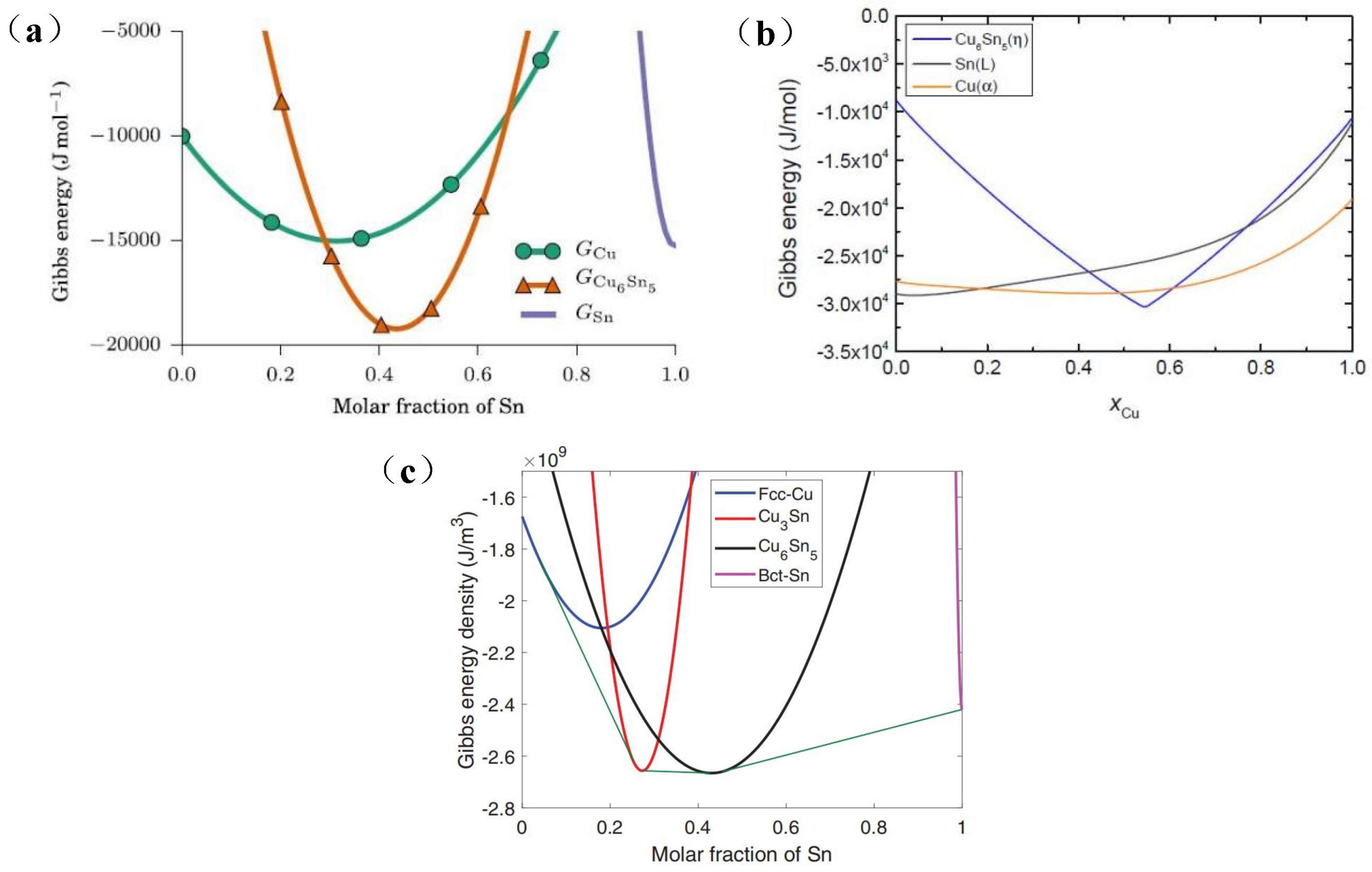
Generally, the multi-phase field model studying the evolution of microstructure involves three phases, Cu(S), liquid Sn(L), and η-Cu6Sn5 with multiple variants, whose structures are characterized by a set of non-conserved order parameters since the reaction is diffusion controlled. The premise of most phase field modeling is to determine whether the phase transition process can occur, that is, whether the free energies of the reacting phases and their products have intersection in the relative phase diagrams [9,16,21,22,23,24]. Figure 4 shows the chemical free energy of Cu(S), liquid Sn (L), and η-Cu6Sn5 during reaction under different conditions. The calculation of the free energy curves is based on the thermodynamic databases of the corresponding phases and IMCs from Thermo-Calc software, a powerful tool for the calculation of phase diagrams according to different needs and purposes [25]. The energy curve of η-Cu6Sn5 with large curvature at clearly reflects its stoichiometric feature.
2.2. Thermodynamic Parameters
The thermodynamic parameter formulas of the Cu-Sn binary system are summarized as follows according to the above free energy calculation database. It should be noted that the free energies of pure elements vary at different temperature ranges as noted in the parentheses following the relative expression. Table 1 shows the generally applicable thermodynamic parameters in most phase-field models for the formation and growth of IMCs in the Cu-Sn binary system [26]. What reactions happen and what phases or IMCs form depend on the specific conditions and needs.
Thermodynamic parameters in the Cu-Sn binary system are present in Table 2. It can be seen that these parameters (they correspond to the “” in the phase field model as mentioned in Section 2.3.2) are only relative to temperature. These results may have slight errors due to artificial calculation or measurements which is a normal phenomenon and does not affect the application of the data.
Other solder specific properties such as diffusivity, mobility, and interface energy must be introduced into the models through phenomenological parameters, which are determined based on experimental and theoretical information.
2.3. Phase Field Modeling
2.3.1. Nucleation of IMCs
A proper nucleation mechanism is necessary for the nucleation of IMCs due to the field theory of self-consistent phase fields. There are mainly two types of nucleation in the formation process of IMCs in micro-interconnects: classical nucleation [20] and noise nucleation [16]. Classical nucleation theory applies discrete Poisson probability distributions to describe the probability of nucleation events at a particular point in time or space. This method was originally proposed by Simmons [28] and used in the classical phase field equation to replace the Langevin noise. The probability for the (heterogeneous) nucleation of a new phase at an arbitrary point in space and time is determined by thermodynamic and kinetic factors such as local driving forces for the nucleation of the new phase as well as interfacial energies that act as barriers to the nucleation. The stochastic nature of nucleation is then approximated by unity “minus” the zero-event probability of a Poisson distribution, which is applied to replace the Langevin noise [29]. The expression of Poisson nucleation probability and nucleation rate I are as follows [22,23]:
where is the time interval over which the probability of nucleation is to be determined, while v represents the volume over which the nucleation probability is calculated [30]:
where σ is the interface energy, is the nucleation barrier, θ is the contact angle, and I0 is the nucleation rate constant. Equation (4) is the classical theoretical formula of IMCs’ nucleation in micro-interconnect. The nucleation of IMCs is determined by probability. Noise nucleation refers to Langevin or stochastic noise terms to describe the thermal fluctuation of order parameters, which is usually appended to the end of the phase field evolution equation. In general, the noise term ξ follows a Gaussian distribution and satisfies the fluctuation dissipation theorem [31]:
where is the Boltzmann constant, is the temperature, and is the symmetric part of the mobility . The above equations correspond to non-conservative and conservative field variables, respectively. The origin of the noise term is related to the microscopic degrees of freedom, such as thermal vibrations, which transforms the statistical expression back into microscopic form. The nucleation of IMCs will be random as one chooses the noise nucleation method.
2.3.2. Evolution Equations
A phase field model must first describe the microstructure by using a set of conserved and/or non-conserved field variables. Second, the evolution of these field variables must be determined by applying the temporal and spatial evolution of the field variables. The morphology evolution and growth kinetics of IMCs with interfacial reaction of the Cu-Sn binary system were studied by the multi-phase field model. Phase field models on IMCs in solders are generally derived from the work of Steinbach [32,33,34] et al., which are applicable to the formation and growth of IMCs in micro-interconnects. In the interface reaction, a general model of the total free energy of a chemically heterogenous system that involves interfacial, bulk, elastic, and electrical interaction is [16,34]
where , ,, and denote the chemical free energy, interfacial energy, elastic energy and electric field energy of the system, respectively. One can also expand thermal gradient field [7], magnetic field [35], and plastic field [21] according to the demand, which are not the main objects in this work. and are temperature-dependent and represent the temperature field. Usually, these two terms are expressed in the same phase field evolution equation. Moreover, the Kim–Kim–Suzuki (KKS) model is employed in the phase field model by considering the interface as a mixture of phases with equal chemical potentials [16] (+), since the formation of IMCs is a second phase precipitation process controlled by diffusion. Additionally, the elastic field is usually represented in the simulation of the formation kinetics of Cu6Sn5 to solve the problem of different variation evolution laws, since the phase field simulation cannot solve the plastic deformation problem at present. is the electrical field at last.
The chemical free energy density of Cu and liquid Sn are available in the binary CALPHAD database [36] and can be expressed as
where xi is the conserved order parameter or atomic fraction of species , and s the Gibbs energy of the pure element in the chemical phase r. The last term corresponds to the excess Gibbs energy, which can be written by the Redlich–Kister polynomial [27]:
where is the temperature-dependent interaction parameters in the binary system.
Due to the stoichiometric nature of η-Cu6Sn5, the chemical free energy was described as a temperature dependent single value instead of a continuous function of composition [37,38]. The description causes a difficulty for any phase field model because the variational derivative of free energy functional with respect to composition is not available. To resolve the issue, many investigators follow the work of Moelans [38,39,40,41] by treating IMCs such as η-Cu6Sn5 and ε-Cu3Sn as a chemical compound with small solubility and adopting a two sublattice model . The chemical free energy of η-Cu6Sn5 is expressed based on the compound energy formulation [18]:
where and are site fractions of species i in sublattice I and II, respectively, is the Gibbs energy of formation of the compound or the so-called end member phases, and m and n give the ratio of sites on the two sublattices, which are 0.545 and 0.455, respectively.
The order parameters are constrained by . The total free energy functional is represented as [39]
The governing equation of non-conserved order parameters was derived as [7]
where Np is the local number of coexisting phases, is a step function which is equal to 1 when the phase exists and is otherwise equal to 0, is the mobility of the interface between phases and , and z is the Langevin noise terms describing thermal fluctuations of the order parameters [10]. The time-evolution of the conserved order parameter or atomic fraction is governed by the Cahn–Hilliard equation:
The elastic strain energy functional is formulated by the micro-elasticity theory derived from Hooke’s law [16]:
where is the elastic stiffness tensor, and is the eigenstrain.
The term in square brackets represents the negative atomic flux of Cu defined in the laboratory frame of reference and is the corresponding chemical mobility.
The electrical field is expressed as [42]
where is the Avogadro number, e is the natural charge of an electron, is the electronic potential, and is the effective nuclear charge of the phases.
Equations (11), (14) and (15) correspond to terms in Equation (7) of total free energy, respectively, which is the phase field equation representing the evolution of IMC Cu6Sn5 in micro-interconnect. Parameters such as m and n, free energy, and interaction coefficient can be modified as it is used to simulate the formation of other IMCs.
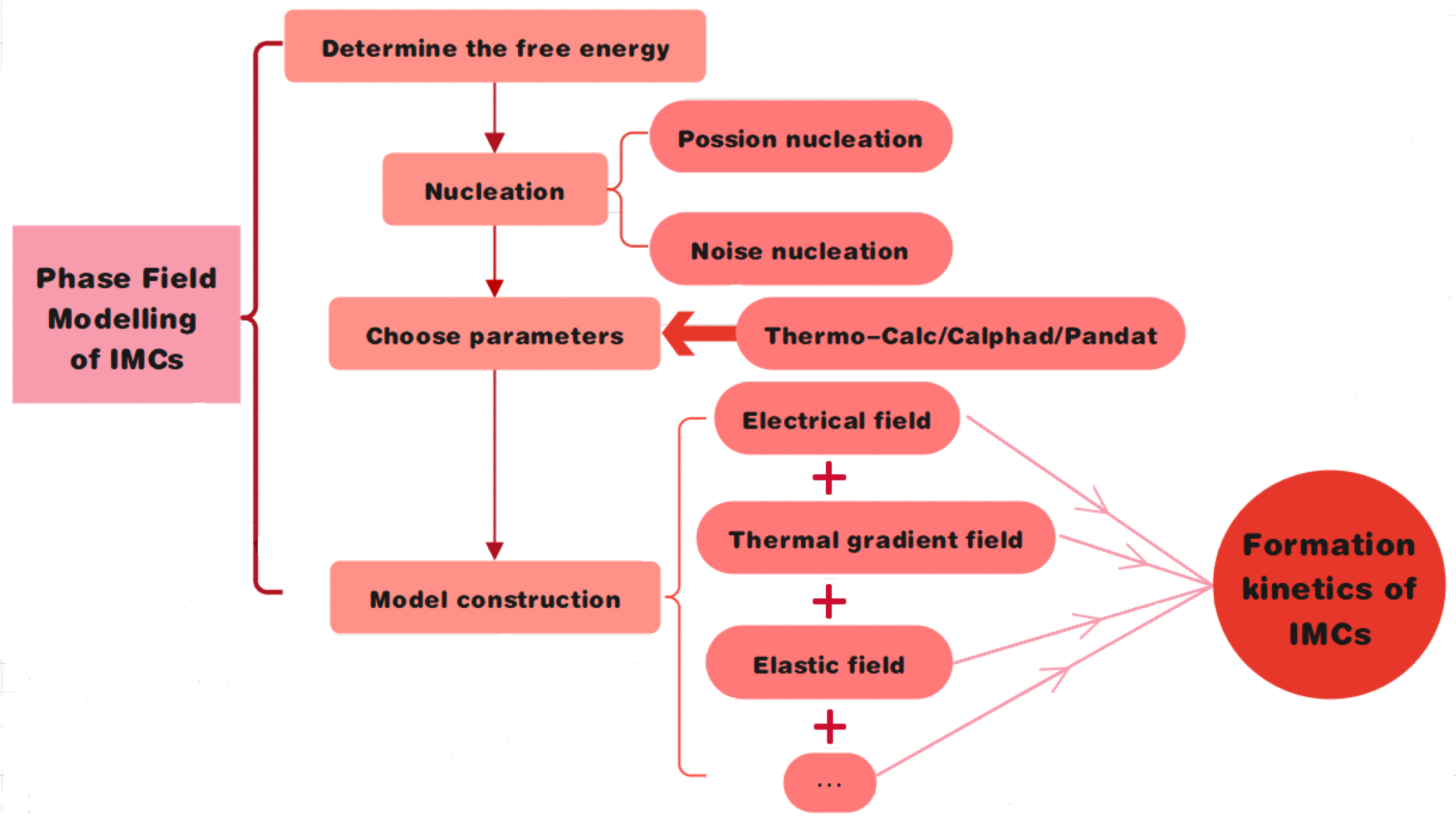
Figure 5 shows the schematic flow chart of the formation mechanism simulated by the phase field method. Firstly, the free energy curves of Cu, Sn, and the relative IMC should be obtained to ensure that the reaction that produces η-Cu6Sn5 and ε-Cu3Sn can happen; secondly, a proper nucleation should be chosen according to the conditions and needs; then, appropriate thermodynamic parameters needs to be chosen to establish a proper simulation model of IMCs; finally, the thermal, stress, and electrical field can be coded one by one in the phase field model.
Park [23] et al. investigated the evolution of IMC layers in the Cu/Sn solder system under electromigration conditions by a multi-phase field formalism through considering the concurrent evolution of the Cu3Sn and Cu6Sn5 IMC layers. It turned out that back- stress resulting from the non-equilibrium vacancy generation due to diffusive flux imbalance among the individual diffusants (Cu and Sn) played a fundamental role in the evolution of the IMC layers, and the simulations and experiments showed nice qualitative agreement. It can be deduced from their work that there are interactions between micro- voids and IMCs, and they interact with each other due to the diffusion of Cu and Sn under thermal–electrical–stress effects, which is really complex in 3DIC.
Ke [16] et al. investigated pattern formation during interfacial reactions in between Liquid Sn and two types of unidirectional Cu substrates, (001) and (111), by using a combination of crystallographic analysis, the theory of micro-elasticity, and phase field simulations. The simulation results showed that each symmetry-related η-Cu6Sn5 variant grew along the direction of best atomic site matching with the substrates. Simulation predictions in their work also demonstrated excellent agreements with experimental observations. It can be concluded from their investigation that η-Cu6Sn5 variants will precipitate along the fit directions which take on the lowest energy for their stable characteristics. This team also found that heteroepitaxial constraints led to spatial alignment of η-Cu6Sn5 variants, which may shed light on the fact that most research works on η-Cu6Sn5 did not show variant features, under which condition no heteroepitaxial growth took place.
Kunwar [7] et al. integrated neural network analysis with the multi-phase field method to quantify the mechanism of thermo-migration at the cold side of a solder-substrate system. Data on heats of transport, temperature difference, and the growth rate constant of IMCs were obtained from multiple FEM (Finite Element Modeling) simulations, and the FEM-generated dataset was employed in the neural network. The growth rate constant predicted by machine learning was tallied with the experimental values. The heat conduction and phase field equations were solved using FEM which was innovative and more efficient than the phase field calculation. However, it should be noted that the accuracy of the dataset generated by FEM is still questionable before it is employed in the neural network.
Durga [22] et al. used a phase field model for multi-phase systems that can treat diffusion, elastic, and especially plastic deformation to study the problem of the growth of intermetallic phases in solder joints undergoing mechanical deformation. Reuss–Sachs and Voigt–Taylor models were combined to describe the plastic part, which was essentially superior to the Khachaturyan scheme applied by most previous studies. It is well known that the behaviors of real materials probably lie between full inheritance of plastic deformation and no inheritance at all. The plastic part in their work necessitated the development of models allowing for the partial inheritance of plastic deformation, which can be adapted in future studies that need to couple the plastic deformation in phase field model of IMCs’ growth.
3. Future Research Aspects
3.1. Interactions between IMCs and Micro-Voids
The structure and morphology of the Cu6Sn5 and Cu3Sn IMC layers should be investigated quantitively since they control the integrity of microelectronic interconnects. At the same time, the formation and accumulation of vacancies in Cu/Cu3Sn interfaces also play a key role in the reliability of 3DIC devices. In fact, IMCs and micro voids generally form concurrently due to the combined functions of thermal, electrical, and stress fields. In other words, there must be interactions between IMCs and vacancies, which is the absolute factor affecting solder joint reliability. In the phase field model, the interactions between IMCs and voids can be coupled together in spite of their distinguished sizes, positions, and characteristics if they are under the same thermal, electrical, and stress fields. Clarity of the interactions between IMCs and voids can be helpful to further elucidate the mechanism of solder joint failure led by interfacial phases and vacancy evolution.
3.2. Couple Multiple Simulation Methods
Multi-scale modeling is a trend in the field of computational material science, not only in the application of the phase field simulation in formation of IMCs and vacancies. The first-principles calculations can provide plastic/elasticity tensors and potential energies; the diffusion number of Cu and Sn atoms during the soldering process can be obtained by molecular dynamics; one can obtain the stress and strain distribution by FEM calculation under the thermos–electro–mechanical fields through which the formation site of IMCs and voids can be predicted. The combination of these approaches will provide a better estimation for the lifetime of solder joints. These simulation methods all can be properly coupled with the phase field models to interpret and predict more deeply the formation and growth of IMCs; they can provide information that cannot be obtained in the phase field simulation alone. Which method is chosen depends on the practical use.
3.3. Quantitative Prediction of Growth of IMCs
The future phase field model should be able to quantitatively capture the kinetic features such as the volume and thickness of the IMC layer according to conditions such as temperature, electron wind, or/and electric current density so as to control the proper thickness of IMCs in industrial production. It is also clear that plastic effects must be considered in the phase field model to obtain realistic results. Additionally, since, in phase field simulations, the width of the interfaces is usually artificially enlarged to limit the computational requirements, the effect of this excess energy can become excessively high which is inconsistent with reality. The difficulty in narrowing the gap between the simulated results and the actual situation should be overcome.
Moreover, since the thickness of the IMC layer can be reduced by adding stabilizing elements such as Al [46] and nanoparticles such as CeO2 [47] in the tin solder, future phase field simulations or calculations should consider building a multi-elements system coupling other alloying elements and additives to interpret mechanisms. Relative phase field simulation can shed light on the growth kinetics of interactions between alloying elements and IMCs, which cannot be achieved by experimental tools alone. Otherwise, the quantitative relationship between alloying elements and IMCs should also be considered so as to obtain more actual results that can serve as a guide to experiment and production.
4. Conclusions
Phase field modeling on formation and growth of IMCs generally follows four steps: (1) determine the free energy curves of the reaction phases and the productive phases; (2) choose proper thermal dynamic parameters; (3) determine a fit nucleation mechanism; (4) construct the evolution equations on thermal, electrical, and stress fields, etc. The fourth step can also be divided into several sub-steps, approached one by one, in order to make sure that each step is reasonable and correct. The sequence of second and third steps can be exchanged since this will not affect the modeling. In order to achieve more accurate results in phase field simulations of IMCs, their interactions with micro voids and other simulation approaches should be considered and they are both promising aspects.
Author Contributions
Conceptualization, H.L. and J.S.; methodology, J.S.; validation, J.S. and X.L.; formal analysis, L.Z. and H.W.; investigation, L.Z. and J.S.; writing-original draft preparation, J.S. and Y.Z.; writing-review and editing, J.S. and C.T.; visualization, J.S.; supervision, H.B.; project administration, H.B. and L.Z.; funding acquisition, H.B. and L.Z. All authors have read and agreed to the published version of the manuscript.
Funding
This research was funded by Applied Basic Research Foundation of Yunnan Province, grant number 202101BC070001-010 and Chuncheng Project III.
Data Availability Statement
The data presented in this study are available upon request from the corresponding author. The data are not publicly available due to technical or time limitations.
Acknowledgments
The authors are grateful to Hao Wang, Lingyan Zhao, and Hailong Bai for their contribution to the discussion.
Conflicts of Interest
The authors declare no conflict of interest.
References
- Dušek, K.; Bušek, D.; Veselý, P.; Pražanová, A.; Plaček, M.; Re, J.D. Understanding the effect of reflow profile on the metallurgical properties of tin–bismuth solders. Metals 2022, 12, 121. [Google Scholar] [CrossRef]
- Rahim, K.; Mian, A. A review on laser processing in electronic and MEMS packaging. J. Electron. Packag. 2017, 139, 030801. [Google Scholar] [CrossRef]
- Attari, V.; Ghosh, S.; Duong, T.; Arroyave, R. On the interfacial phase growth and vacancy evolution during accelerated electromigration in Cu/Sn/Cu microjoints. Acta. Mater. 2018, 160, 185–198. [Google Scholar] [CrossRef] [Green Version]
- Ahn, B. Emerging interconnection technology and Pb-Free solder materials for advanced microelectronic packaging. Metals 2021, 11, 1941. [Google Scholar] [CrossRef]
- Wieser, C.; Walnsch, A.; Hügel, W.; Leineweber, A. The monoclinic lattice distortion of η′-Cu6Sn5. J. Alloy. Compd. 2019, 794, 491–500. [Google Scholar] [CrossRef]
- Roy, A.; Luktuke, A.; Chawla, N.; Ankit, K. Predicting the Cu6Sn5 growth kinetics during thermal aging of Cu-Sn solder joints using simplistic kinetic modeling. J. Electron. Mater. 2022, 51, 4063–4072. [Google Scholar] [CrossRef]
- Kunwar, A.; Hektor, J.; Nomoto, S.; Coutinho, Y.A.; Moelans, N. Combining multi-phase field simulation with neural network analysis to unravel thermomigration accelerated growth behavior of Cu6Sn5 IMC at cold side Cu–Sn interface. Int. J. Mech. Sci. 2020, 184, 105843. [Google Scholar] [CrossRef]
- Liang, S.B.; Ke, C.B.; Huang, J.Q.; Zhou, M.B.; Zhang, X.P. Phase field simulation of microstructural evolution and thermomigration-induced phase segregation in Cu/Sn58Bi/Cu interconnects under isothermal aging and temperature gradient. Microelectron. Reliab. 2019, 92, 1–11. [Google Scholar] [CrossRef]
- Kunwar, A.; Coutinho, Y.A.; Hektor, J.; Ma, H.; Moelans, N. Integration of machine learning with phase field method to model the electromigration induced Cu6Sn5 IMC growth at anode side Cu/Sn interface. J. Mater. Sci. Technol. 2020, 59, 203–219. [Google Scholar] [CrossRef]
- Li, Y.; Fu, G.; Wan, B.; Yan, X.; Zhang, W.; Li, W. Phase-field modelling of lead-free solder joint void growth under thermal-electrical coupled stress. J. Electron. Mater. 2022, 51, 259–272. [Google Scholar] [CrossRef]
- Lee, L.M.; Mohamad, A.A. Interfacial reaction of Sn-Ag-Cu lead-free solder alloy on Cu: A review. Adv. Mater. Sci. Eng. 2013, 2013, 123697. [Google Scholar] [CrossRef] [Green Version]
- Zu, Z.; Chen, D.; Zhang, X.; Bai, H.L.; Leng, C.Y.; Gan, G.Y.; Yan, J.K. On the initial stages and growth process of intermetallic compounds at Cu/Sn interface: A MD simulation and experimental study. Comp. Mater. Sci. 2022, 208, 111349. [Google Scholar] [CrossRef]
- Zou, H.F.; Yang, H.J.; Zhang, Z.F. Morphologies, orientation relationships and evolution of Cu6Sn5 grains formed between molten Sn and Cu single crystals. Acta. Mater. 2008, 56, 2649–2662. [Google Scholar] [CrossRef]
- Yang, A.; Duan, Y.; Li, C.; Yi, J.; Peng, M. Theoretical explorations of structure, mechanical properties, fracture toughness, electronic properties, and thermal conductivity of Ag-doped η′-Cu6Sn5. Intermetallics 2022, 141, 107437. [Google Scholar] [CrossRef]
- Bernal, J.D. The Complex Structure of the Copper–Tin Intermetallic Compounds. Nature 1928, 122, 54. [Google Scholar] [CrossRef]
- Ke, J.H.; Gao, Y.; Kao, C.R.; Wang, Y. Pattern formation during interfacial reaction in-between liquid Sn and Cu substrates—A simulation study. Acta. Mater. 2016, 113, 245–258. [Google Scholar] [CrossRef] [Green Version]
- Zhong, Y.; An, R.; Ma, H.; Wang, C.Q. Low-temperature-solderable intermetallic nanoparticles for 3D printable flexible electronics. Acta. Mater. 2019, 162, 163–175. [Google Scholar] [CrossRef]
- Shang, P.J.; Liu, Z.Q.; Pang, X.Y.; Li, D.X.; Shang, J.K. Growth mechanisms of Cu3Sn on polycrystalline and single crystalline Cu substrates. Acta. Mater. 2009, 57, 4697–4706. [Google Scholar] [CrossRef]
- Liu, B.; Tian, Y.; Wang, C.; An, R.; Wang, C.Q. Ultrafast formation of unidirectional and reliable Cu3Sn-based intermetallic joints assisted by electric current. Intermetallics 2017, 80, 26–32. [Google Scholar] [CrossRef]
- Tang, Y.; Luo, S.; Li, Z.; Hou, C.; Li, G. Morphological Evolution and Growth Kinetics of Interfacial Cu6Sn5 and Cu3Sn Layers in Low-Ag Sn-0.3Ag-0.7Cu-xMn/Cu Solder Joints During Isothermal Ageing. J. Electron. Mater. 2018, 47, 5913–5929. [Google Scholar] [CrossRef]
- Hektor, J.; Ristinmaa, M.; Hallberg, H.; Hall, S.A.; Iyengar, S. Coupled diffusion-deformation multiphase field model for elastoplastic materials applied to the growth of Cu6Sn5. Acta. Mater. 2016, 108, 98–109. [Google Scholar] [CrossRef] [Green Version]
- Durga, A.; Wollants, P.; Moelans, N. Phase-field study of IMC growth in Sn-Cu/Cu solder joints including elastoplastic effects. Acta. Mater. 2020, 188, 241–258. [Google Scholar] [CrossRef]
- Park, M.S.; Arróyave, R. Concurrent nucleation, formation and growth of two intermetallic compounds (Cu6Sn5 and Cu3Sn) during the early stages of lead-free soldering. Acta. Mater. 2012, 60, 923–934. [Google Scholar] [CrossRef]
- Sun, J.; Li, X.X.; Zhang, J.H.; Wang, G.; Yang, M.; Wang, H.; Xu, D.S. Phase field modeling of formation mechanism of grain boundary allotriomorph in β→α phase transformation in Ti-6Al-4V alloy. Acta. Metall. Sin. 2020, 56, 1113–1122. [Google Scholar]
- Sun, J.; Zhang, Y.T.; Wang, P.; Ye, Z.F.; Li, D.Z. Effect of N on the microstructure and mechanical properties of high Si martensitic heat-resistant steels. Acta. Metall. Sin. (Engl. Lett.) 2014, 27, 573–584. [Google Scholar] [CrossRef]
- Dinsdale, A.T. Sgte data for pure elements. Calphad 1991, 15, 317–425. [Google Scholar] [CrossRef]
- Moon, K.-W.; Boettinger, W.J.; Kattner, U.R.; Biancaniello, F.S.; Handwerker, C.A. Experimental and thermodynamic assessment of Sn-Ag-Cu solder alloys. J. Electron. Mater. 2000, 29, 1122–1136. [Google Scholar] [CrossRef]
- Simmons, J.P.; Shen, C.; Wang, Y. Phase field modeling of simultaneous nucleation and growth by explicitly incorprating nucleation events. Scripta. Mater. 2000, 43, 935–942. [Google Scholar] [CrossRef]
- Qi-Sen, H.; Li, L.; Xiu-Xun, W.; Jin-Fu, L. Solidification behaviors of undercooled Ni-P alloys. Acta. Phys. Sin. 2012, 61, 166401–166407. [Google Scholar] [CrossRef]
- Park, M.S.; Arroyave, R. Formation and growth of intermetallic compound Cu6Sn5 at early stages in lead-free soldering. J. Electron. Mater. 2010, 39, 2574–2582. [Google Scholar] [CrossRef] [Green Version]
- Najafi, A. The fluctuation-dissipation theorem of colloidal particle’s energy on 2D periodic substrates: A monte carlo study of thermal noise-like fluctuation and diffusion like Brownian motion. J. Phys. Conf. Ser. 2014, 510, 012025. [Google Scholar] [CrossRef]
- Steinbach, I.; Pezzolla, F.; Nestler, B.; Sedklberg, M.; Ptieler, R.; Schmitz, G.J.; Rezende, J.L.L. A phase field concept for multiphase systems. Phys. D 1996, 94, 135–147. [Google Scholar] [CrossRef]
- Steinbach, I.; Pezzolla, F. A generalized field method for multiphase transformations using interface fields. Phys. D 1999, 134, 385–393. [Google Scholar] [CrossRef]
- Xiong, H.; Huang, Z.; Conway, P. Effects of Stress and Electromigration on Microstructural Evolution in Microbumps of Three-Dimensional Integrated Circuits. IEEE Trans. Device Mater. Reliab. 2014, 14, 995–1004. [Google Scholar] [CrossRef] [Green Version]
- Wang, Y.Z.; Li, J. Phase field modeling of defects and deformation. Acta. Mater. 2010, 58, 1212–1235. [Google Scholar] [CrossRef]
- Liang, S.B.; Ke, C.B.; Zhou, M.B.; Zhang, X.P. Coupled Phase Field and Finite Element Modeling of Void Evolution and Physical Property Change of Micro Flip-Chip Solder Joints under Electromigration and Elastic Stress Field. In Proceedings of the 18th International Conference on Electronic Packaging Technology, Harbin, China, 16–19 August 2017; p. 1631. [Google Scholar]
- Liang, S.B.; Ke, C.B.; Ma, W.J.; Zhou, M.B.; Zhang, X.P. Numerical simulations of migration and coalescence behavior of microvoids driven by diffusion and electric field in solder interconnects. Microelectron. Reliab. 2017, 71, 71–82. [Google Scholar] [CrossRef]
- Sun, J.; Qi, M.; Zhang, J.H.; Li, X.X.; Wang, H.; Ma, Y.J.; Xu, D.S.; Lei, J.F.; Yang, R. Formation mechanism of α lamellae during β→α transformation in polycrystalline dual-phase Ti alloys. J. Mater. Sci. Technol. 2021, 71, 98–108. [Google Scholar] [CrossRef]
- Moelans, N. A quantitative and thermodynamically consistent phase-field interpolation function for multi-phase systems. Acta. Mater. 2011, 59, 1077–1086. [Google Scholar] [CrossRef] [Green Version]
- Moelans, N.; Blanpain, B.; Wollants, P. An introduction to phase-field modeling of microstructure evolution. Calphad 2008, 32, 268–294. [Google Scholar] [CrossRef]
- Moelans, N.; Godfrey, A.; Zhang, Y.; Juul, J.D. Phase-field simulation study of the migration of recrystallization boundaries. Phys. Rev. B 2013, 88, 054103. [Google Scholar] [CrossRef] [Green Version]
- Park, M.S.; Gibbons, S.L.; Arróyave, R. Phase-field simulations of intermetallic compound evolution in Cu/Sn solder joints under electromigration. Acta. Mater. 2013, 61, 7142–7154. [Google Scholar] [CrossRef]
- Liu, G.P.; Zhang, J.Y.; Lei, M.; Li, Y.L.; Li, X.W. A comparative study of the diffuse-interface model and sharp-interface model in the soldering related wetting spreading systems. Metals 2019, 9, 944. [Google Scholar] [CrossRef] [Green Version]
- Park, M.S.; Gibbons, S.L.; Arróyave, R. Computational investigation of the evolution of intermetallic compounds affected by microvoids during the solid-state aging process in the Cu-Sn system. J. Electron. Mater. 2013, 42, 999–1009. [Google Scholar] [CrossRef]
- Sun, J.; Liang, H.X.; Sun, S.F.; Hu, J.T.; Teng, C.Y.; Zhao, L.Y.; Bai, H.L. Pattern formation by spinodal decomposition in ternary lead-free Sn-Ag-Cu solder alloy. Metals 2022, 12, 1640. [Google Scholar] [CrossRef]
- Koleňák, R.; Augustin, R.; Martinkovič, M.; Chachula, M. Comparison study of SAC405 and SAC405+0.1%Al lead free solders. Solder. Surf. Mt. Technol. 2013, 25, 175–183. [Google Scholar] [CrossRef]
- Li, Z.; Tang, Y.; Guo, Q.; Li, G. A diffusion model and growth kinetics of interfacial intermetallic compounds in Sn-0.3Ag-0.7Cu and Sn-0.3Ag-0.7Cu-0.5CeO2 solder joints. J. Alloy. Compd. 2020, 818, 152893. [Google Scholar] [CrossRef]
Figure 1.
(a) Schematic diagram of solder wetting process; (b) top view of Cu6Sn5 andCu3Sn grains formed on (001)Cu single crystal at reflow at 260 °C for 600 s [13]; (c) cross section view of Cu/Sn/Cu structure and IMCs [11].
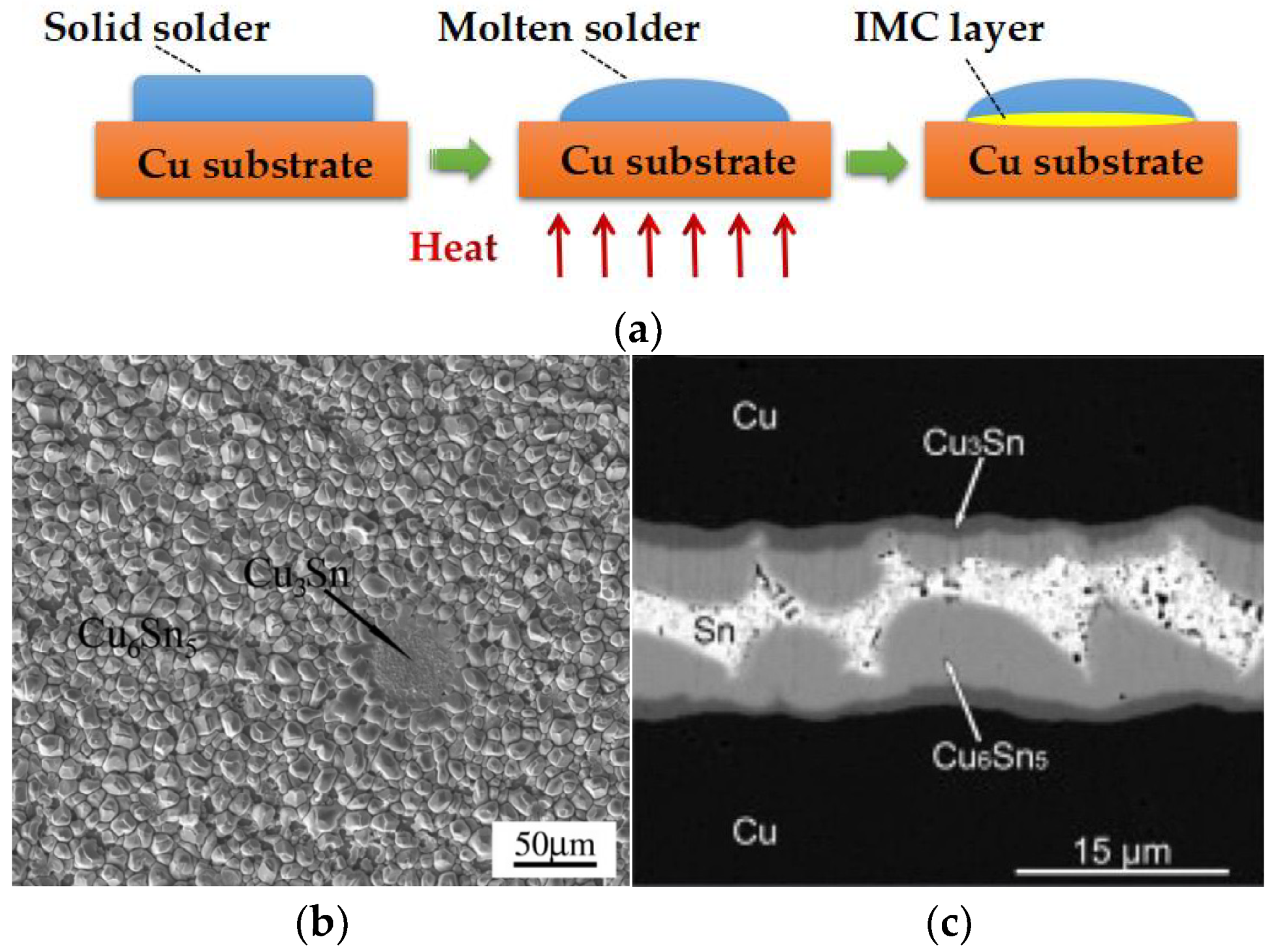
Figure 2.
Schematic illustrations showing the 2D atomic site correspondence at the interface between (a) η-Cu6Sn5 and (001) Cu; (b) η-Cu6Sn5 and (111) Cu. The shaded area in the hexagonal lattice η-Cu6Sn5 shows the lattice plane in parallel with the Cu surface [16].
Figure 2.
Schematic illustrations showing the 2D atomic site correspondence at the interface between (a) η-Cu6Sn5 and (001) Cu; (b) η-Cu6Sn5 and (111) Cu. The shaded area in the hexagonal lattice η-Cu6Sn5 shows the lattice plane in parallel with the Cu surface [16].
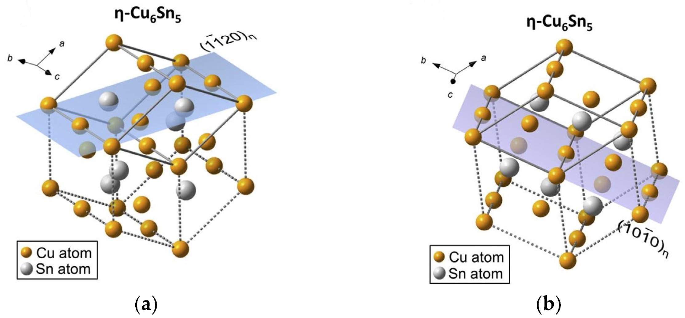
Figure 3.
Scheme of the interfacial reaction of solder/Cu during solder reflow: (a) dissolution of the Cu substrate; (b) supersaturation of the molten solder layer with Cu; (c) formation of the scallop-type Cu6Sn5 at the interface; and (d) Cu3Sn emerges between Cu6Sn5/Cu with prolonged soldering.
Figure 3.
Scheme of the interfacial reaction of solder/Cu during solder reflow: (a) dissolution of the Cu substrate; (b) supersaturation of the molten solder layer with Cu; (c) formation of the scallop-type Cu6Sn5 at the interface; and (d) Cu3Sn emerges between Cu6Sn5/Cu with prolonged soldering.

Figure 4.
Plots showing the chemical free energy of Cu (s), liquid Sn (L), and η-Cu6Sn5 during reaction 6Cu + 5Sn→Cu6Sn5: (a) free energy evolution with Sn mole fraction as a function of composition at 25 °C [21]; (b) free energy evolution with Cu mole fraction as a function of composition at 250 °C [16]; (c) free energy evolution with Sn mole fraction as a function of composition in which condition both η-Cu6Sn5 and ε-Cu3Sn precipitated [22].

Figure 5.
Flow chart of kinetics of formation of IMCs by the phase field method.


| Phases | Temperature Range | Free Energy |
|---|---|---|
| Sn (Pure) | ||
| Cu (Pure) | ||
| Sn (Liquid) | ||
| Sn * (F.C.C.) | ||
| Sn (B.C.C.) | ||
| Sn (H.C.P.) | ||
| Cu (Liquid) | ||
| Cu (B.C.C.) | ||
| Cu (B.C.T.) | ||
| Cu6Sn5 | -- | |
| Cu3Sn | -- |
* Many reactions such as L→Sn+Cu6Sn5 involve the metastable phases in the Cu-Sn system under the interactions of thermal, electrical, and force fields. Therefore, FCC and BCT in the above table respectively represent face-centered cubic or body-centered foursquare phases.
Table 2.
Thermodynamic parameters in Cu-Sn binary system [27].
Table 2.
Thermodynamic parameters in Cu-Sn binary system [27].
| Phases | Thermodynamic Parameters |
|---|---|
| Liquid | |
| F.C.C | |
| B.C. T |
Publisher’s Note: MDPI stays neutral with regard to jurisdictional claims in published maps and institutional affiliations. |
© 2022 by the authors. Licensee MDPI, Basel, Switzerland. This article is an open access article distributed under the terms and conditions of the Creative Commons Attribution (CC BY) license (https://creativecommons.org/licenses/by/4.0/).
Share and Cite
MDPI and ACS Style
Sun, J.; Zhao, L.; Liang, H.; Zhang, Y.; Li, X.; Teng, C.; Wang, H.; Bai, H. A Review on Phase Field Modeling for Formation of η-Cu6Sn5 Intermetallic. Metals 2022, 12, 2043. https://doi.org/10.3390/met12122043
AMA Style
Sun J, Zhao L, Liang H, Zhang Y, Li X, Teng C, Wang H, Bai H. A Review on Phase Field Modeling for Formation of η-Cu6Sn5 Intermetallic. Metals. 2022; 12(12):2043. https://doi.org/10.3390/met12122043
Chicago/Turabian StyleSun, Jia, Lingyan Zhao, Huaxin Liang, Yao Zhang, Xuexiong Li, Chunyu Teng, Hao Wang, and Hailong Bai. 2022. "A Review on Phase Field Modeling for Formation of η-Cu6Sn5 Intermetallic" Metals 12, no. 12: 2043. https://doi.org/10.3390/met12122043
Note that from the first issue of 2016, this journal uses article numbers instead of page numbers. See further details here.