2. Materials and Methods
The OK Autrod 308LSi ESAB welding wire was used to produce the pilot workpieces. According to EN ISO 14343-2017, the material’s yield strength is 400 MPa. The wire’s chemical composition is given in
Table 1. The material of this chemical composition refers to austenitic stainless steels. The wire’s ferrite number (FN) is 8, which denotes that the content of the ferritic phase in the deposited metal is within a range of 3–8% (~4.5%).
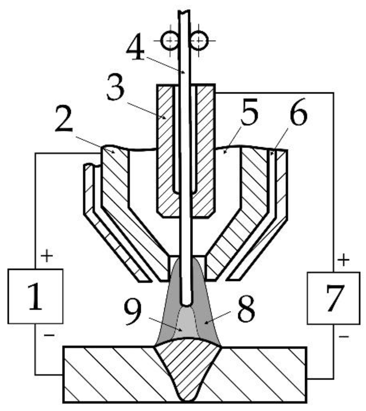
The deposition welding was carried out using a plasma device for Plasma-MIG deposition welding designed at Perm National Research Polytechnic University. The principle of the facility is shown in
Figure 1. A KEDR-400 power supply was used as the power supply for the consumable electrode, and a Kedr Arc-319 power supply for TIG welding was used as the power supply for the plasma arc.
The Plasma-MIG layer-by-layer depositions of wire material and deformation treatment are implemented on one platform using a CNC machine with an integral SA7401H AIRPRO air hammer manufactured by Airpro Industry Corp. (New Taipei, Taiwan). The principle of the facility is shown in
Figure 2.
The deposition welding of the walls with and without interpass work hardening (peening) was carried out via the selected deposition regime: plasma arc current Ia = 120 A; consumable electrode arc current Ie = 210 A; arc voltage U = 23–24 V; wire feed speed Vwire = 6.6 m/min; torch movement speed Vdep = 90 cm/min; volume of argon supplied to the welding torch Qshield = 7.5 L/min; volume of argon supplied to plasma forming nozzle Qpl = 2.5 L/min. Peening was carried out via a previously selected regime: air hammer movement speed Vham = 100 mm/min (linear number of strokes N/L = 28.2 strokes/mm at the standard hammer stroke frequency N = 2820 strokes/min); the hammer tip was a semisphere with a radius of R = 20 mm; stroke energy E = 19.74 J. The hammer’s pressing force created by the air cylinder was 300 N. The temperature at which the peening of the deposited layers was conducted was T = 250–300 °C.
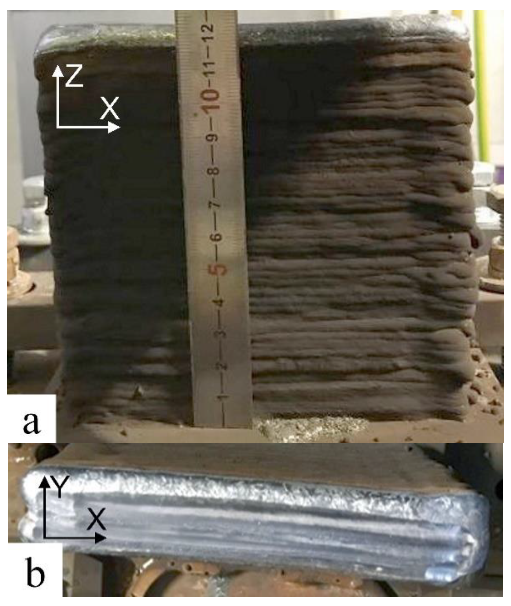
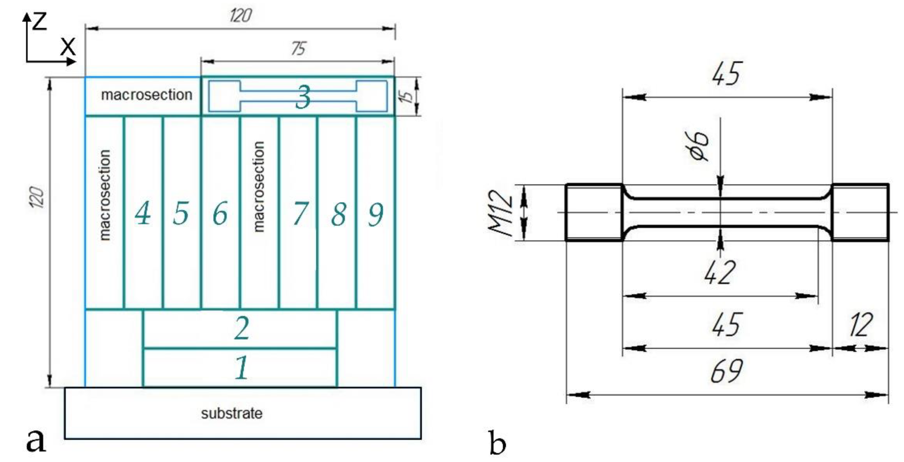
Workpiece samples for the study of the structure and mechanical characteristics of the deposited metal were produced in the form of a flat wall (
Figure 3), where X is the horizontal direction along the deposition direction, and Z is the vertical.
Microstructural studies were performed for the polished sections cut out in the transverse and longitudinal directions of the deposition welding of the wall workpiece. To reveal the microstructure, Vasiliev’s chemical agent was used to treat the polished sections (hydrochloric acid 500 mL, sulphuric acid 250 mL, blue vitriol 100 g, water 500 mL). The studies were conducted on an Altami CM0745-T stereomicroscope (LLC Altami, Saint Petersburg, Russia) and an Altami MET 1T inverted light microscope (LLC Altami, Saint Petersburg, Russia) with a magnification up to 1000× using the Altami Studio 3.5 software (LLC Altami, Saint Petersburg, Russia). To study the microstructure and determine the local chemical composition of the phases, we used two scanning electron microscopes. A JEOL JSM 6490 microscope (JEOL Ltd., Tokyo, Japan) with an Inca X-sight Oxford Instruments attachment (JEOL Ltd., Tokyo, Japan) for local X-ray spectral microanalysis was used at 20 kV and a HITACHI S-3400N high-resolution (3–10 nm) scanning electron microscope (Hitachi Ltd., Tokyo, Japan) equipped with a Bruker EDS XFlash Detektor (Bruker Corp., Billerica, MA, USA) 4010 was used at 5 kV.
The phase composition of the samples was studied using a Shimadzu XRD-7000 X-ray diffractometer (Shimadzu, Kyoto, Japan). To separate the Kβ component of X-ray radiation, a monochromator was used during the analysis. The X-ray photography conditions were as follows: the range of the scan angle 2θ from 40 to 120 deg, Cu X-ray tube, tube voltage 30 kV, tube current 30 mA, scan speed 1 deg/min, scan step 0.01 deg, DS 1 deg, SS 1 deg, RS 0.15 mm. The X-ray diffraction patterns were processed using the PANalytical X’Pert HighScore Plus Ver.2.1 software (Malvern Panalytical Ltd., Malvern, UK). The phase composition of the samples under analysis was determined using the ICDD PDF-2 Release 2012 database.
Hardness was tested by the Vickers method using an automated micro- and microhardness tester Emco-Test Durascan 50 (EMCO-TEST Prüfmaschinen GmbH, Kuchl, Austria), ser. No. 119, under a load of 100 g. One hundred measurements were made in the form of a 5 × 20 net: 5 width measurements with a step of 0.1 mm and 20 depth measurements with a step of 0.05 mm.
To find the mechanical properties, samples were cut out from the walls produced by deposition welding in accordance with
Figure 4.
The largest variation in characteristics during additive growth is usually observed for samples in the vertical direction. So, three specimens and six specimens in the vertical have been tested for the tensile strength for each wall. Tensile tests were performed at room temperature with a strain rate of 1 × 10
−3 s
−1 using an Instron 8801 servohydraulic system (Instron, Norwood, MA, USA) on standard (ISO 6892-1:2016) samples with a diameter of 5 mm and a gauge length of 25 mm (
Figure 4b).
4. Discussion
Based on the results of the study, the features of the formation of macro- and microstructure and phase composition in the workpiece from the 308LSi alloy produced by Plasma-MIG hybrid welding with the use of layer-by-layer cold working have been revealed.
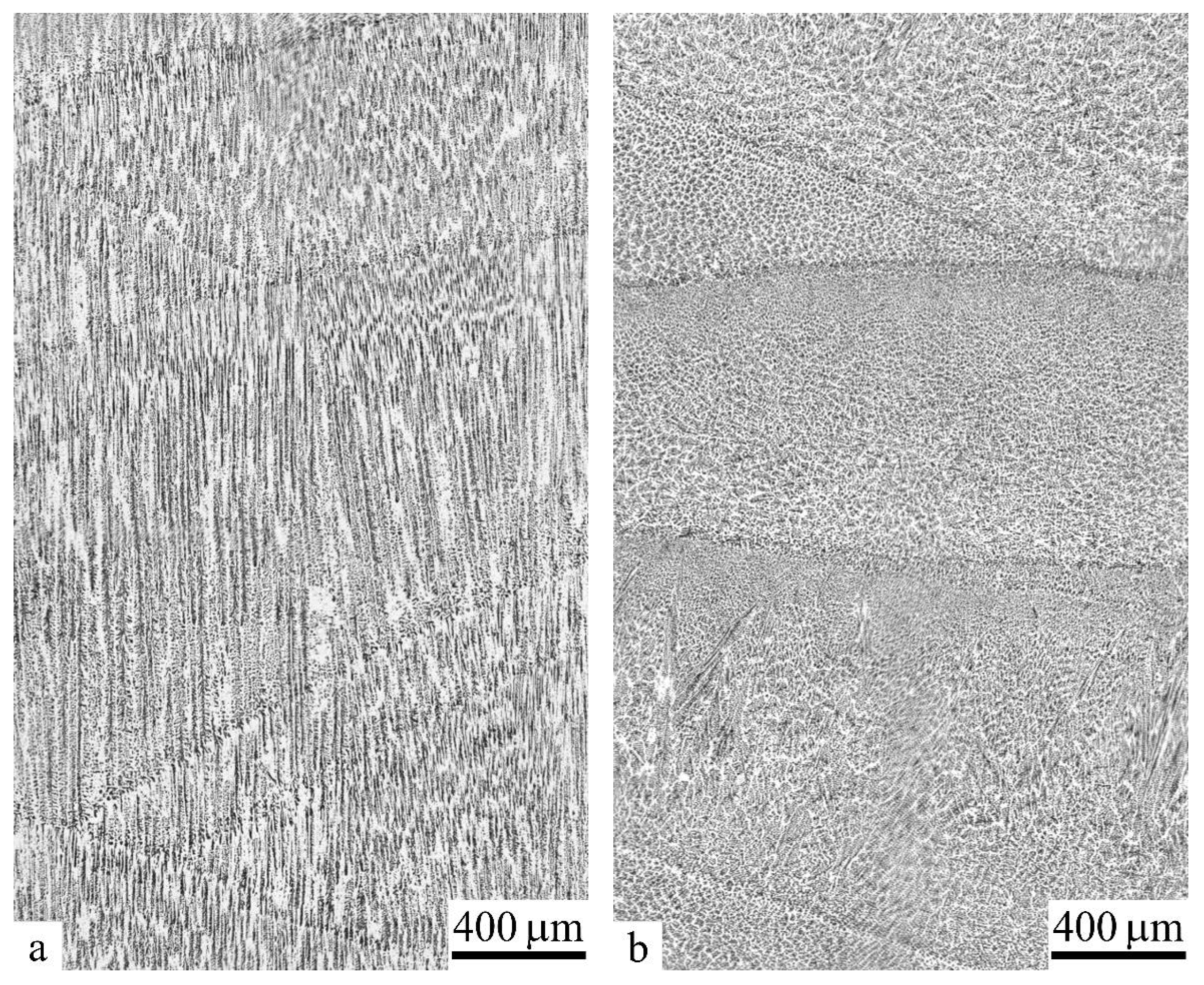
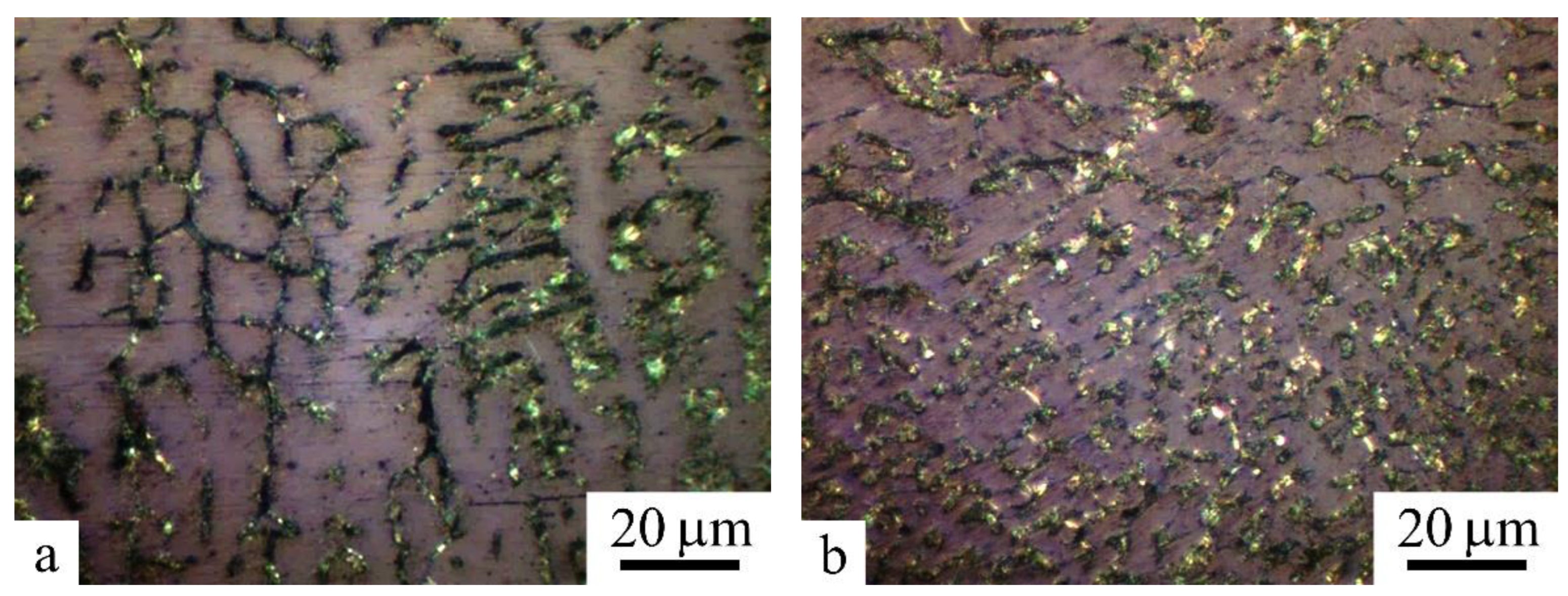
First, in both cases a dendritic microstructure is formed, characteristic of layer-by-layer wire deposition welding of austenitic steels [
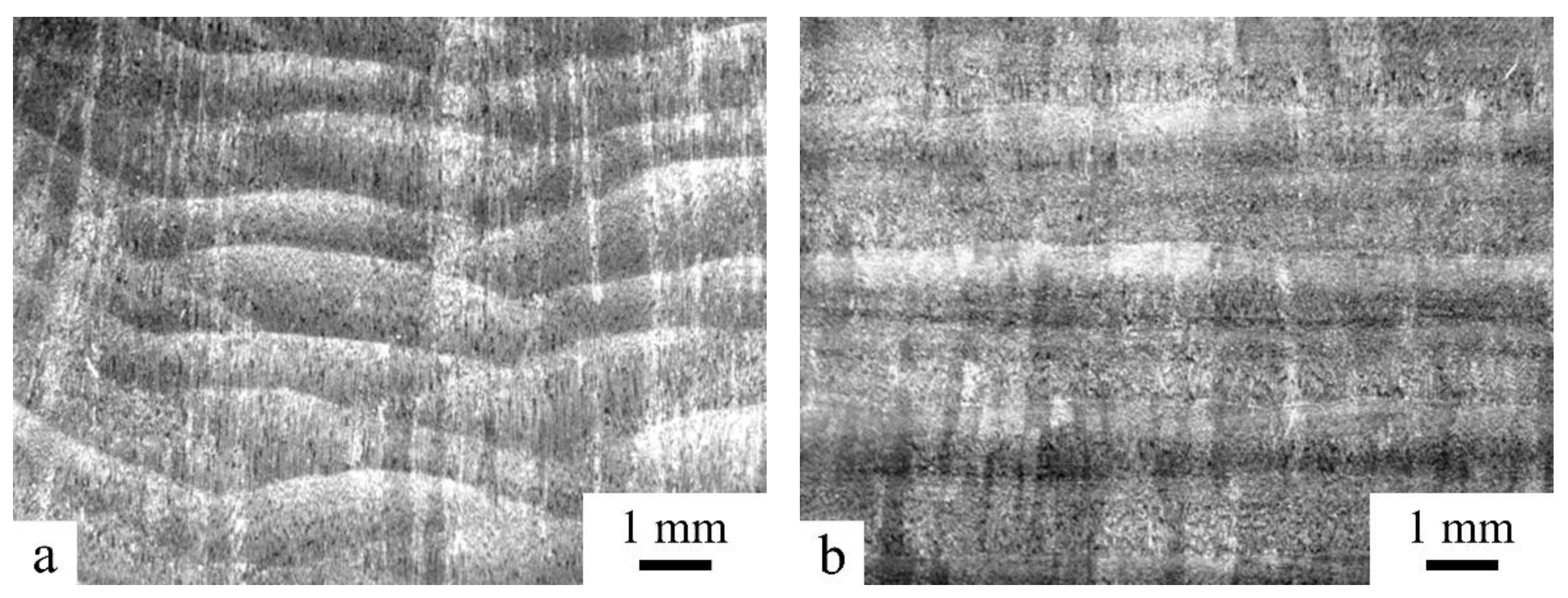
2]. A difference in the shape of the dendrites was revealed. In particular, in the regular regime of deposition welding (without layer-by-layer peening) the dendrites are characterized by a columnar shape and grow through the fusion zone (
Figure 6a). Such structures were observed in [
2] during deposition welding by WAAM. The introduction of cold working after the cooling of a layer led to the formation of dendrites with predominantly a more equiaxed shape (
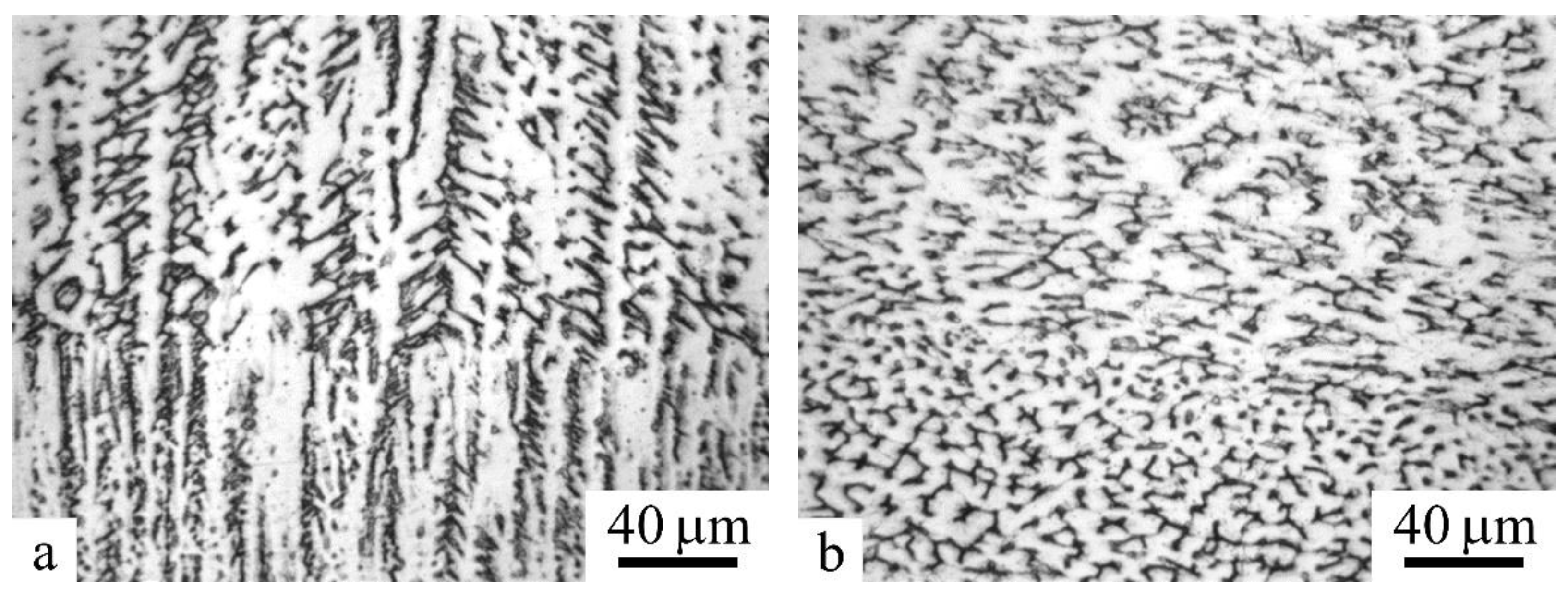
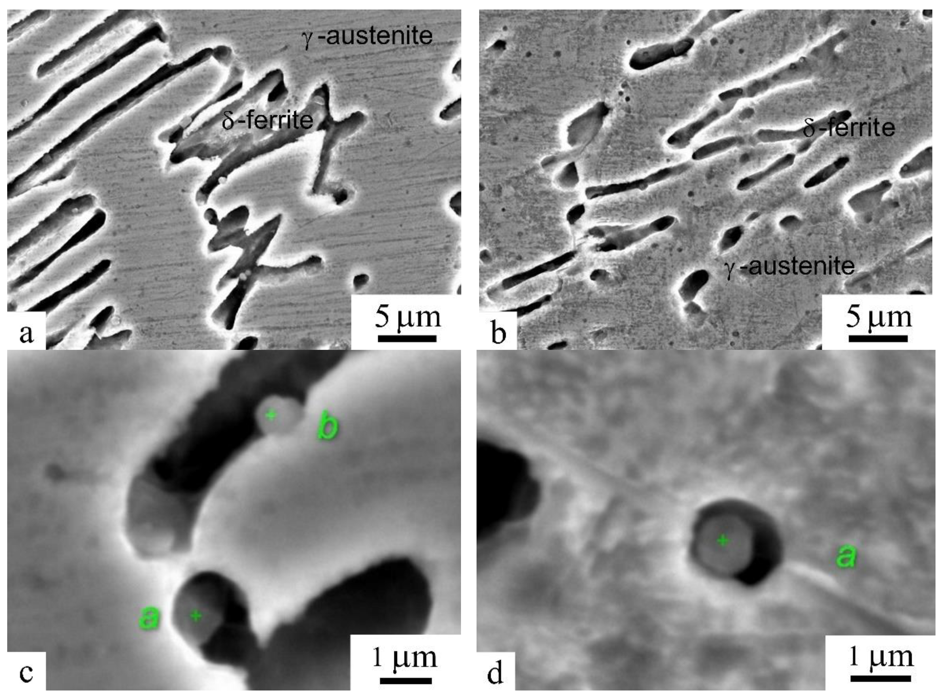
Figure 6b). The microstructure of the metal inside the layer in the workpieces produced using peening is characterized by a less pronounced anisotropy and metallographic texture (
Figure 7b). Apparently, during cold working, the level of stress and the dislocation density in the surface layer increase, which promotes a change in the direction of crystallite growth in the next layer and, as a consequence, a refinement of the microstructure.
Therefore, during the crystallization of a new deposited layer, the number of crystallization centers increases and, as a result, a more dispersed microstructure is formed than in the case of deposition welding without peening.
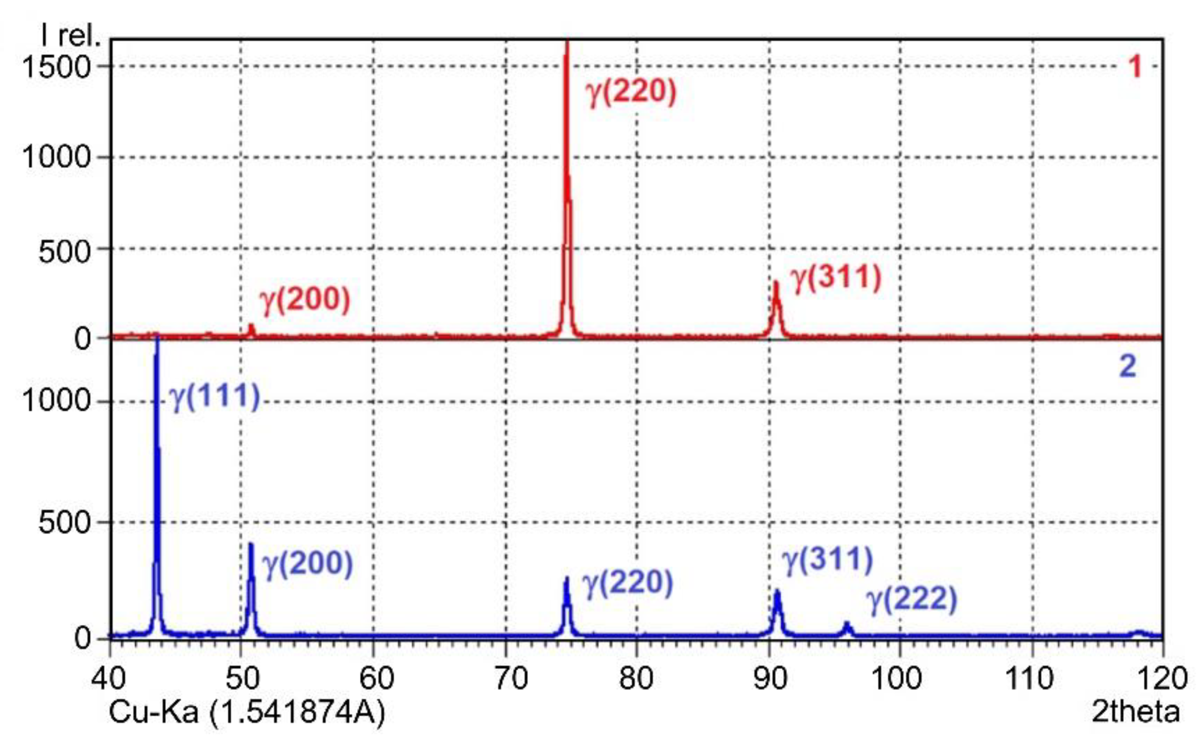
The studies of the phase composition of the metal produced via different regimes demonstrate that the crystallized metal consists of austenite and carbides that precipitated during cooling from the Cr-rich austenite. In the X-ray diffraction pattens of the samples produced using cold peening, peaks from δ-ferrite are observed (
Figure 10). It is known from the literature data [
22,
23] that the crystallization of austenitic steels (like 308L) in a range of temperatures between the liquidus and the solidus occurs via the following mechanism: austenite is formed as the first phase, then eutectic ferrite precipitates in the interdendritic space. Eutectic ferrite is formed from the last portions of the Cr- and Ni-rich liquid phase via the liquidation mechanism:
Correspondingly, the structure of the crystallized metal represents austentite’s dendrites (γ) and residual delta-ferrite (δ) at the boundaries of dendrites and cells. Normally, the content of residual δ-ferrite in a deposited metal does not exceed 8% [
23]. It can be assumed that residual δ-ferrite is present in both samples produced with and without peening. Apparently, in both cases peaks in the X-ray diffraction pattens had low intensity. Meanwhile, according to [
2] the content of residual δ-ferrite under different parameters of the WAAM treatment of the 316 L steel was from 13% to 17%.
The data of the X-ray phase analysis data correlate with the results of the microstructural studies on optical and scanning microscopes and indicate that, at the final stage of crystallization, carbide compounds precipitate from the last portions of the liquid phase in the layers deposited using both process variants. Apparently, the formation of fine-dispersed carbides may be associated with a continuous thermal cycle. It appears that, in the process of the deposition of a new layer, the preceding layer experiences a high-temperature heating below the solidus temperature. Such heating may promote carbide precipitation in interdendritic spaces enriched with carbon and chromium, predominantly at the boundaries between dendrites and cells. Due to the fact that, in the case of deposition welding with layer-by-layer cold working, a more dispersed structure is formed, the carbide size is smaller and they are more uniformly distributed in the structure (
Figure 11).
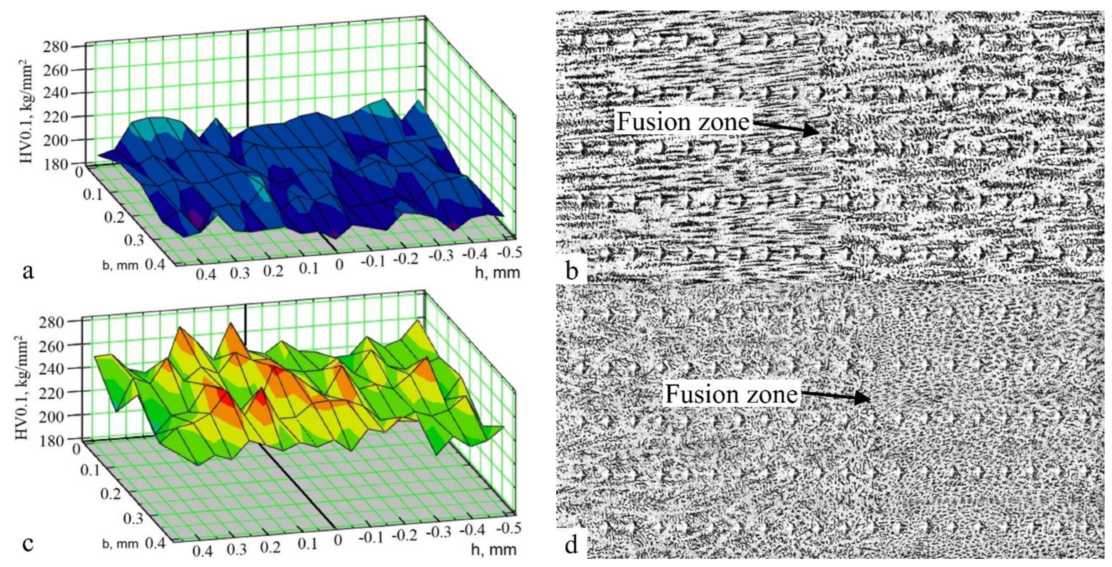
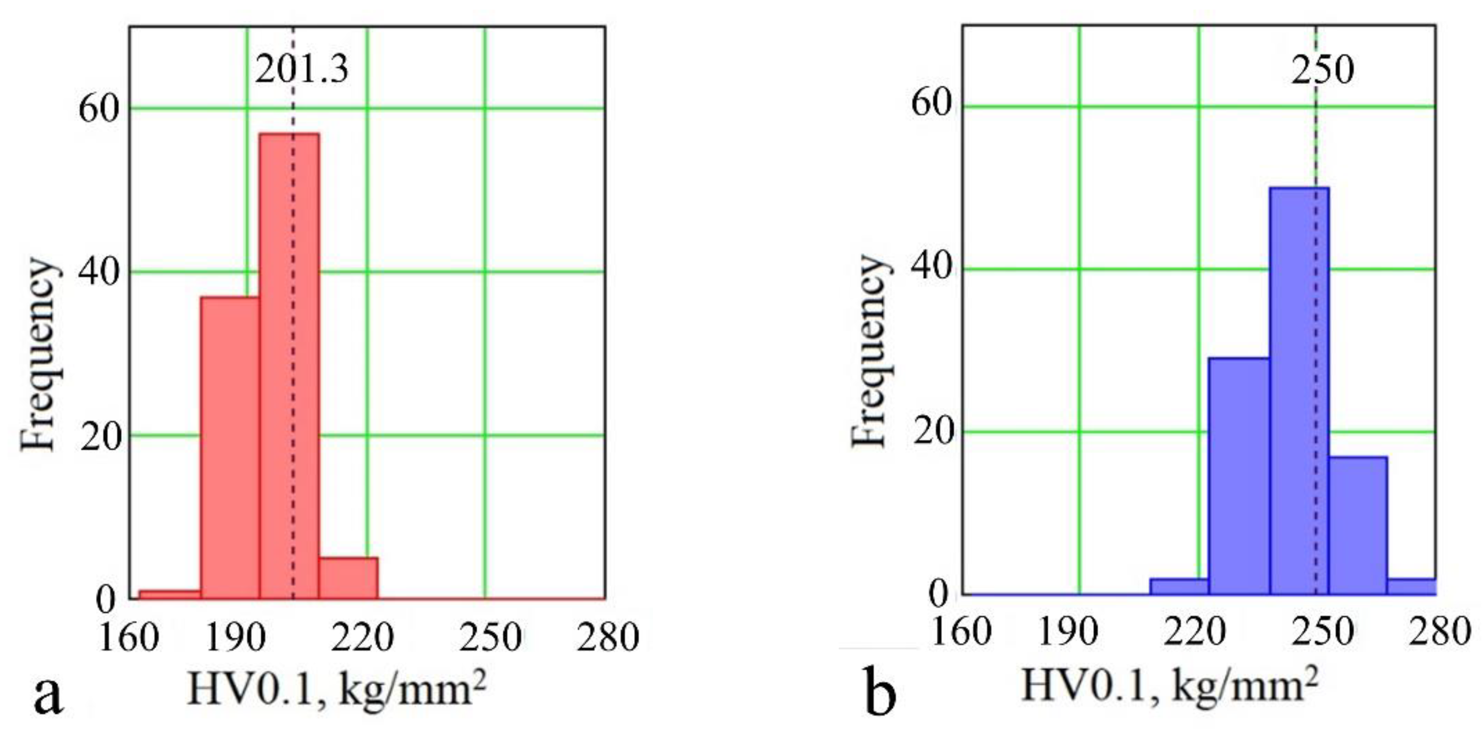
The results of the microhardness testing of the samples produced by both variants of deposition welding show that when layer-by-layer cold peening is used, the total level of hardness increases by 50 HV due to an increase in the microstructure’s degree of dispersion. At the same time, a less uniform hardness distribution is observed in the case of deposition welding with peening (
Figure 14). This could evidently be attributed to the different degrees of dispersion of the microstructure inside a layer and in the near-boundary regions corresponding to the surface of the filler wire subjected to cold working (
Figure 7b). Such a regularity was observed earlier in [
16].
The tensile mechanical tests of the samples demonstrate that the use of layer-by-layer cold peening during the plasma wire deposition welding Plasma-MIG leads to the enhancement of the strength characteristics while preserving the ductility characteristics at a high level as compared to deposition welding without peening (UTS 710 and 555 MPa, respectively). The anisotropy of properties does not increase either. The use of the subsequent heat treatment of the obtained samples would perhaps additionally reduce the scatter of the characteristic values in the vertical and horizontal directions, which will be necessarily investigated in subsequent works. It should be noted that the ultimate tensile strength of the 316 L steel metal produced by the conventional WAAM method is within a range of 520–570 MPa [
2], which correlates with the level of strength of the sample produced in the present work without layer-by-layer peening (598 MPa).
Thus, the results obtained in the present study demonstrate that the Plasma-MIG hybrid process that combines arc deposition welding with a consumable electrode and plasma deposition welding is a promising method for manufacturing large-sized parts. The introduction of deformation treatment in the process of the layer-by-layer synthesis of a workpiece leads to grain size reduction, a decrease in the anisotropy of the macro- and microstructure and, consequently, an increase in the mechanical characteristics of a workpiece. This research area is in its development stage and opens prospects for producing workpieces with a minimum machining allowance and high service characteristics. At the same time, its wide application in industry requires solving various materials-science and processing tasks. This includes the tasks of providing the precision of a workpiece and the specified structure and properties of a metal, such as fusion penetration depth, area of the fusion zone between layers, rates of metal heating and cooling, time for which a metal is in the molten state, chemical composition of metal layers, loss of alloying elements, and so forth. It should be noted that layer-by-layer shot peening reduces the productivity of the process (by a factor of 1.5–2), but this fact can fade into the background in the manufacture of critical products, when the level and reproducibility of the mechanical properties of the material of the part are of paramount importance.
Author Contributions
Conceptualization, T.O. and D.T.; Investigation, A.D., A.G. and A.P.; Methodology, T.O. and I.S.; Writing–original draft, T.O.; Writing–review & editing, D.T. and I.S. All authors have read and agreed to the published version of the manuscript.
Funding
This research was funded by Russian Science Foundation (RSF), grant number 21-19-00715 “Control of microstructure, strength, residual stresses and geometry distortions in hybrid additive manufacturing” (Agreement No. 21-19-00715 dated 20 March 2021).
Institutional Review Board Statement
Not applicable.
Informed Consent Statement
Not applicable.
Data Availability Statement
Not applicable.
Acknowledgments
The authors are grateful to the Center for Common Use “Nanotech” of Ufa State Aviation Technical University.
Conflicts of Interest
The authors declare no conflict of interest.
References
- DebRoy, T.; Wei, H.L.; Zuback, J.S.; Mukherjee, T.; Elmer, J.W.; Milewski, J.O.; Beese, A.M.; Wilson-Heid, A.; De, A.; Zhang, W. Additive manufacturing of metallic components—Process, structure and properties. Prog. Mater. Sci. 2018, 92, 112–224. [Google Scholar] [CrossRef]
- Long, P.; Wen, D.; Min, J.; Zheng, Z.; Li, J.; Liu, Y. Microstructure Evolution and Mechanical Properties of a Wire-Arc Additive Manufactured Austenitic Stainless Steel: Effect of Processing Parameter. Materials 2021, 14, 1681. [Google Scholar] [CrossRef] [PubMed]
- Ding, D.; Pan, Z.; Cuiuri, D.; Li, H. Wire-feed additive manufacturing of metal components: Technologies, developments and future interests. Int. J. Adv. Manuf. Technol. 2015, 81, 465–481. [Google Scholar] [CrossRef]
- Wu, B.; Pan, Z.; Ding, D.; Cuiuri, D.; Li, H.; Xu, J.; Norrish, J. A review of the wire arc additive manufacturing of metals: Properties, defects and quality improvement. J. Manuf. Process. 2018, 35, 127–139. [Google Scholar] [CrossRef]
- Köhler, M.; Fiebig, S.; Hensel, J.; Dilger, K. Wire and Arc Additive Manufacturing of Aluminum Components. Metals 2019, 9, 608. [Google Scholar] [CrossRef]
- Lee, H.; Park, S.; Kang, C.-Y. Effect of plasma current on surface defects of plasma-MIG welding in cryogenic aluminum alloys. J. Mater. Process. Technol. 2015, 223, 203–215. [Google Scholar] [CrossRef]
- Lee, H.-K.; Chun, K.-S.; Park, S.-H.; Kang, C.-Y. Control of surface defects on plasma-MIG hybrid welds in cryogenic aluminum alloys. International. Int. J. Nav. Archit. 2015, 7, 770–783. [Google Scholar] [CrossRef]
- Guo, Y.; Pan, H.; Ren, L.; Quan, G. An investigation on plasma-MIG hybrid welding of 5083 aluminum alloy. Int. J. Adv. Manuf. Technol. 2018, 98, 1433–1440. [Google Scholar] [CrossRef]
- Mamat, S.; Afandi, A.A.M.; Abu Bakar, M.B.; Masri, M.N.; Mohamed, M.; Razab, M.K.A.A.; Tanaka, M. Effect of Plasma Flow in Plasma MIG Welding Process to the Microstructure Refinement at Heat Affected Zone of As-Welded Carbon Steel. Mater. Sci. Forum 2020, 1010, 15–20. [Google Scholar] [CrossRef]
- Harris, I.D. Plasma-MIG Welding, Welding, Brazing, and Soldering. In ASM Handbook; Thomas, D.L.O., Siewert, A., Glen, S.L., Edwards, R., Eds.; ASM International: Cleveland, OH, USA, 1993; Volume 6, pp. 223–225. [Google Scholar]
- Shchitsyn, Y.D.; Terentev, S.A.; Neulybin, S.D.; Artyomov, A.O. Formation of 04Cr18Ni9 steel structure and properties during additive manufacturing of blanks. Int. J. Adv. Manuf. Technol. 2019, 102, 3719–3723. [Google Scholar] [CrossRef]
- Blakhyna, I. Investigation of surfaced press molds made its working resource. Technol. Audit Prod. Reserves 2017, 3, 34–38. [Google Scholar] [CrossRef][Green Version]
- Haghdadi, N.; Laleh, M.; Moyle, M.; Primig, S. Additive manufacturing of steels: A review of achievements and challenges. J. Mater. Sci. 2021, 56, 64–107. [Google Scholar] [CrossRef]
- Knysh, V.V.; Solovej, S.A.; Kuzmenko, A.Z. Effectiveness of strengthening butt welded joints after long-term service by high-frequency mechanical peening. Paton Weld. J. 2014, 11, 42–45. [Google Scholar] [CrossRef]
- Lu, J.Z.; Luo, K.Y.; Zhang, Y.K.; Sun, G.F.; Gu, Y.Y.; Zhou, J.Z.; Ren, X.D.; Zhang, X.C.; Zhang, L.F.; Chen, K.M.; et al. Grain refinement mechanism of multiple laser shock processing impacts on ANSI 304 stainless steel. Acta Mater. 2010, 58, 5354–5362. [Google Scholar] [CrossRef]
- Martina, F.; Williams, S.W.; Colegrove, P.A. Improved microstructure and increased mechanical properties of additive manufacture produced Ti–6Al–4V by interpass cold rolling. In Proceedings of the 24th International Solid Freeform Fabrication Symposium, Austin, TX, USA, 12−14 August 2013. [Google Scholar]
- Baranov, V.N.; Sidelnikov, S.B.; Bezrukikh, A.I.; Zenkin, E.Y. Study of the rolling regimes and mechanical properties of the cold-rolled, annealed and welded semi-products from Al-Mg pilot alloys sparingly alloyed with Sc. Tsvetnye Met. 2017, 9, 91–96. (In Russian) [Google Scholar] [CrossRef]
- Panin, V.E.; Kablov, E.N.; Pleshanov, V.S.; Klimenov, V.A.; Ivanov, Y.F.; Pochivalov, Y.I.; Kibitkin, V.V.; Napryushkin, A.A.; Nekhoroshkov, O.N.; Lukin, V.I.; et al. Effect of ultrasonic impact treatment on the structure and fatigue resistance of VKS-12 high-strength steel welds. Fiz. Mezomekhanika 2006, 9, 85–96. (In Russian) [Google Scholar]
- Shchitsyn, Y.; Kartashev, M.; Krivonosova, E.; Olshanskaya, T.; Trushnikov, D. Formation of Structure and Properties of Two-Phase Ti-6Al-4V Alloy during Cold Metal Transfer Additive Deposition with Interpass Forging. Materials 2021, 14, 4415. [Google Scholar] [CrossRef]
- Brooks, J.A.; Williams, J.C.; Thompson, A.W. Microstructural origin of the skeletal ferrite morphology of austenitic stainless steel welds. Metall. Trans. A 1983, 14, 1271–1281. [Google Scholar] [CrossRef]
- Anisovich, A.G.; Rumyantseva, I.N. Practice of Metallographic Studies of Metals; Belarusskaya Nauka: Minsk, Belarus, 2013; p. 221. (In Russian) [Google Scholar]
- Rajasekhar, K.; Harendranath, C.S.; Raman, R.; Kulkarni, S.D. Microstructural evolution during solidification of austenitic stainless steel weld metals: A color metallographic and electron microprobe analysis study. Mater. Charact. 1997, 38, 53–65. [Google Scholar] [CrossRef]
- Valiente Bermejo, M.A.; Wessman, S. Computational thermodynamics in ferrite content prediction of austenitic stainless steel weldments. Weld World 2019, 63, 627–635. [Google Scholar] [CrossRef]
Figure 1.
Principle of plasma arc welding (deposition welding) with a consumable electrode–Plasma-MIG: 1–plasma arc power supply; 2–non-consumable electrode; 3–contact tip; 4–consumable electrode; 5–plasma gas; 6–shielding gas; 7–power supply for the consumable electrode arc; 8–plasma arc; 9–consumable electrode arc.
Figure 2.
Principle of the facility for implementing Plasma-MIG hybrid welding and layer-by-layer peening.
Figure 3.
View of the workpiece: (a) side view, XZ; (b) the view from above XY.
Figure 4.
Plan of sampling sites for examination and a scheme for cutting out samples for mechanical tests (a) and the drawing of the tensile specimen in millimeters (b).
Figure 5.
Macrostructure of the deposited metal: (a,b)—deposition welding without layer-by-layer peeing, (c,d)—deposition welding with layer-by-layer peening; (a,c)—transverse section, (b,d)—longitudinal section.
Figure 6.
General view of the microstructure of the metal deposited without (a) and with (b) layer-by-layer peening.
Figure 7.
Microstructure of the metal at a boundary between the deposited layers in a sample produced without (a) and with (b) cold peening.
Figure 8.
Microstructure of the deposited metal without (a) and with (b) layer-by-layer peening.
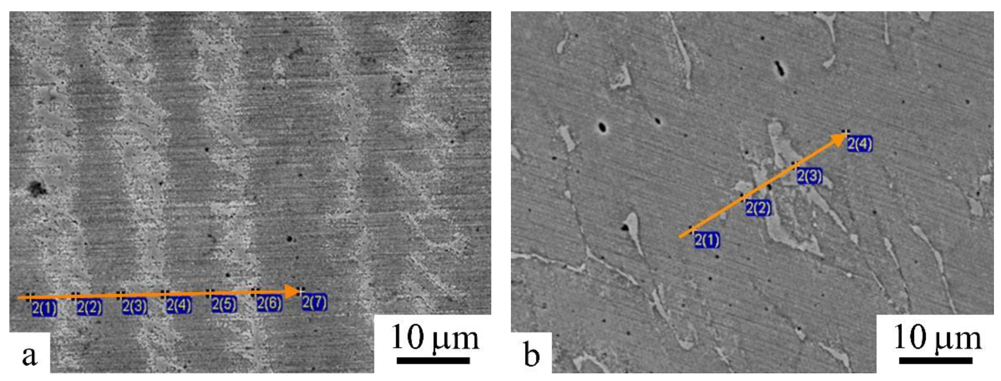
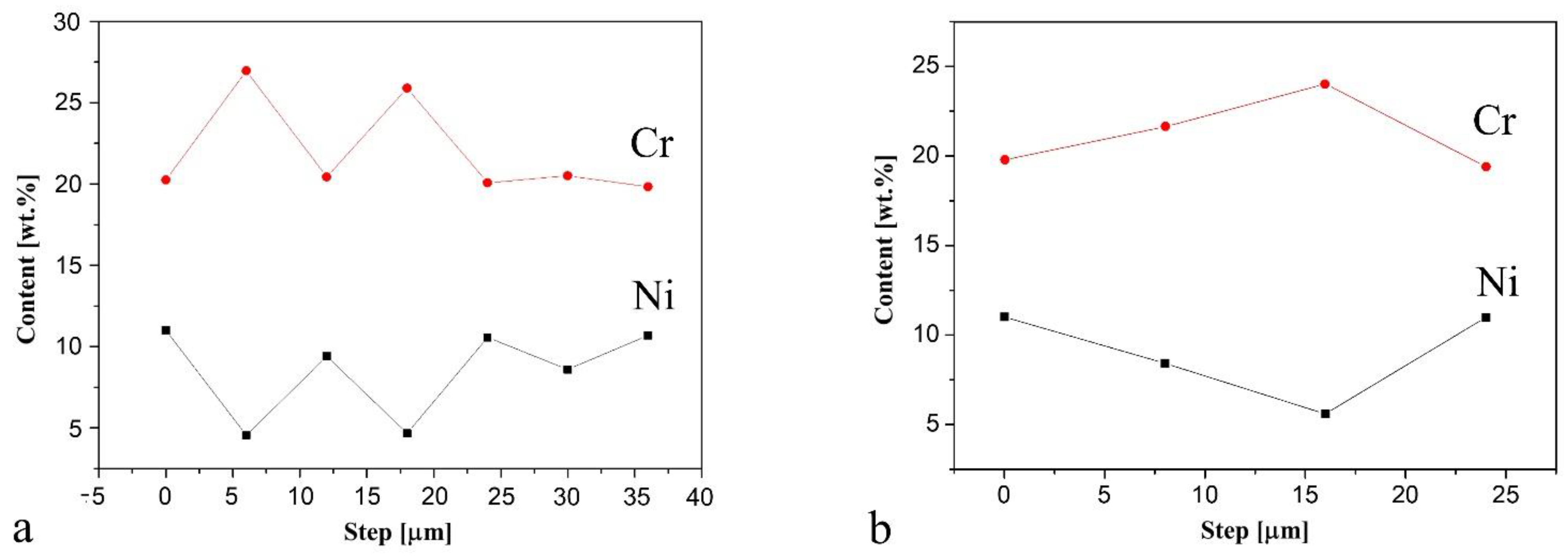
Figure 9.
Distribution of the alloying elements (Cr, Ni) along the EDS lines: (a) deposition welding without peening; (b) deposition welding with peening.
Figure 10.
X-ray diffraction patterns for the steel samples after plasma deposition welding without layer-by-layer peening (line 1) and with layer-by-layer peening (line 2).
Figure 11.
Microstructure inside a layer for the samples after deposition welding without (a) and with (b) layer-by-layer peening. Polarized light.
Figure 12.
SEM images of the microstructure and carbide particles in the metal deposited without peening (a,c) and with peening (b,d).
Figure 13.
Microhardness maps for the transition zone between layers (a,c) and measurement examples (b,d): (a,b)—welding deposition without peening; (c,d)—welding deposition with layer-by-layer peening; h—measurements in layer depth, (b)—measurements in layer width.
Figure 14.
Diagrams of the frequency distribution of the microhardness values: (a)—deposition welding without peening; (b)—deposition welding with layer-by-layer peening.
Table 1.
Chemical composition (wt.%) of the 308LSi wire according to EN ISO 14343-2017.
| C | Mn | Si | Cr | Ni | P | S |
|---|
| ≥0.03 | 1.50–2.10 | 0.65–1.00 | 19.5–21.0 | 9.0–11.0 | ≥0.030 | ≥0.020 |
Table 2.
Microhardness HV0.1 of the samples produced using different process variants.
| Values | Without Layer-by-Layer Deformation | With Layer-by-Layer Deformation |
|---|
| Average value | 201.36 | 250 |
| Minimum value | 180 | 224 |
| Maximum value | 217 | 279 |
| σ–Root-mean-square deviation | 7.16 | 11.35 |
| υ–Variation coefficient (%) | 3.56 | 4.54 |
Table 3.
Results from the testing of the mechanical properties.
| Fabrication Method | Specimen Orientation | UTS
[MPa] | YS0.2
[MPa] | Elongation, δ [%] | Reduction
Area, ψ [%] |
|---|
| Plasma-MIG deposition welding | Z | 555 ± 7 | 295 ± 5 | 34 ± 3 | 72 ± 10 |
| Plasma-MIG deposition welding | X | 560 ± 10 | 300 ± 10 | 50 ± 5 | 60 ± 5 |
| Plasma-MIG deposition welding with layer-by-layer peening | Z | 710 ± 20 | 550 ± 30 | 30 ± 6 | 50 ± 2 |
| Plasma-MIG deposition welding with layer-by-layer peening | X | 740 ± 20 | 570 ± 30 | 36 ± 1 | 56 ± 6 |
| 308LSi according to EN ISO 14343-2017 | - | 570 | 400 | 36 | - |
| AISI 304 L steel according to ASTM A240 (thick sheet) | - | ≥485 | ≥170 | 40 | - |
| Publisher’s Note: MDPI stays neutral with regard to jurisdictional claims in published maps and institutional affiliations. |
© 2022 by the authors. Licensee MDPI, Basel, Switzerland. This article is an open access article distributed under the terms and conditions of the Creative Commons Attribution (CC BY) license (https://creativecommons.org/licenses/by/4.0/).


 ,
, 


