Article

Micro-/Nano-Texturing of Aluminum by Precise Coining for Functional Surface Decoration

1
Surface Engineering Design Laboratory, Shibaura Institute of Technology, Tokyo 144-0045, Japan
2
Komatsu-Seiki Kosakusho, Co., Ltd., Suwa 392-0012, Japan
3
LPS-Works, Co., Ltd., Tokyo 144-0033, Japan
*
Author to whom correspondence should be addressed.
Metals 2020, 10(8), 1044; https://doi.org/10.3390/met10081044
Submission received: 15 June 2020 / Revised: 20 July 2020 / Accepted: 24 July 2020 / Published: 3 August 2020

Abstract

:
The AISI316 austenitic stainless steel die was prepared and nitrided at 673 K for 14.4 ks. Through this low temperature plasma nitriding, the AISI316 die was homogeneously hardened up to 1400 HV within its surface layer of 50 μm. This nitrided AISI316 die was utilized to print the tailored micropattern with nanotextures onto its surface by the femtosecond laser processing. Each micropattern consisted of the tailored segments to have unidirectional nanotextures with different orientations. Each segment was recognized by its intrinsic surface plasmonic brilliance to tailored nanotextures. The CNC (Computer Numerical Control) stamping system was used to coin these micropatterns with nanotextures onto the AA1060 aluminum plates with the thickness of 1 mm. SEM (Scanning Electron Microscopy) and optical microscopy were employed to characterize the original micro-/nano-textures on the AISI316 die as well as the coined nanotextured patterns on the AA1060 plate surfaces.

1. Introduction

Various drawings, fonts, and patterns have been printed onto the metallic sheets, plates, and solids not only for commercial service but also for functional decoration [1]. These things are digitally designed and transformed into CAD (Computer Aided Design) data to directly drive and control the printing and machining tools. In addition to surface coloring by the grating technique [2], the micro-/nano-textures on the metallic plates and products are expected to significantly change the original surface properties and to improve the heat transfer process. The hydrophilic surface of AISI304 plates was modified by the femtosecond laser nanotexturing to be hydrophobic or super-hydrophobic [3,4,5]. The overall heat penetration capacity of an aluminum heat sink was improved by its microtextures [6,7]. The boiling heat transfer process was enhanced by micro-/nano-textures on the pure aluminum and copper devices [8,9,10]. In addition to these nano-texturing effects on the surface and engineering fields, various mini-/micro-/nano-textured metallic sheets and plates are necessary in mass for health-control and medical operations to deal with medicines, polymer parts, cells, viruses, etc. [11,12]. Mini-/micro-textures on the metallic plates provide a visible work-field to preserve the culturing platform; nanotextures yield a space to culture the targeting cells, viruses, and microorganisms [13]. A new printing system is necessary to duplicate the tailored micro- and nano-patterns onto the metallic sheets and plates and to fabricate the functionally decorated devices and parts. Femtosecond laser processing becomes a powerful tooling system to print the microtextures as well as the nanotextures onto any material substrates [14,15,16]. In particular, LIPSS (Laser Induced Periodic Surface Structuring) [17] forms various nanotextured morphologies on the work material surface with different LIPSS-ripple periods in the function of laser beam capacity such as fluence and pulse width in addition to the work surface condition. As surveyed in [18,19,20], this LIPSS process is useful to make nanotexturing onto the punches and dies and to transcribe the tool-surface nanostructures onto the metal, polymer, and oxide-glass products by stamping. Optical property and structure control by femtosecond laser nanotexturing has a direct influence on the decoration on the metallic products [21,22].
In the present paper, the micro-/nano-textured AISI316 dies are fabricated by the femtosecond laser machining to coin the textured punch surface to the aluminum plate by CNC (Computer Numerical Control)-stamping. The low temperature plasma nitriding is employed to preharden the AISI316 substrate as a mother punch with the tailored micro-/nano-textures. In this design of original micro-/nano-patterns, every micropattern consists of geometric unit-segments, which are represented by an assembly of nanopatterns with different orientations. The femtosecond laser machining is employed to print these tailored micro-/nano-patterns as micro-/nano-textures on the mother punch surface. First, 8 × 8 matrix with 64 unit segments is designed by allocating the nanopattern with the specified orientation to each designated segment. This CAD data are transformed into CAM (Computer Aided Machining) data to drive the laser control in the femtosecond laser machining. Six nanotextures are formed onto the specified segment to build up the matrix as an assembly of 64 nanotextured segments. Each segment is color decorated in blue by the surface plasmon intrinsic to each nanotexture. Second, the mother punch with seven microtextures is prepared for precise coining of these microtextures with nanotextures onto the pure aluminum plates. SEM and optical microscopy is utilized to evaluate the micro- and nano-textures of mother punch as well as coined specimens.

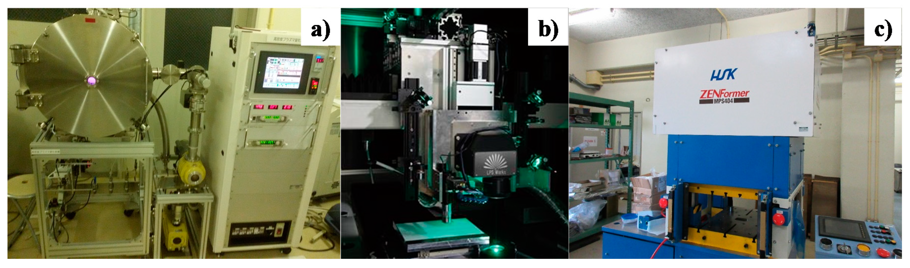
2. Experimental Procedure

AISI316 die substrates with the size of 24 × 14 × 5 mm3 were surface-polished, nitrided, and laser-machined to form these micropatterns with nanotextures. This laser-processed punch was fixed into a cassette die to coin these micropatterns with nanotextures onto pure aluminum plates.
As the first step, the plasma nitriding system in Figure 1a was utilized to nitride the buff-polished AISI316 die substrate at 673 K for 14.4 ks at 70 Pa under the nitrogen-hydrogen mixture gas with the flow rate of 160 mL/min for nitrogen and 30 mL/min for hydrogen, respectively. Although no heat treatment was utilized before nitriding, the hardness of nitrided punch increases up to 1400 HV in average within the nitrided layer thickness of 50 μm. Owing to this nitrogen supersaturation, the average nitrogen solute content becomes 4 mass % homogeneously in the nitrided layer.
A femtosecond laser machining system in Figure 1b is utilized to form the tailored spatial nano-textures onto the nitrided AISI316 punch with the head size of 10 × 20 mm2. The wave length of femtosecond laser was 515 nm, the pulse width was 200 fs, and the pulse repetition rate was 20 MHz. The maximum power in average was 40 W, and the maximum pulse energy was 50 μJ. Hence, the power by irradiation of a single pulse is estimated to be 0.25 GW. The fluence of laser irradiation is constant by 0.61 J/cm2. The beam spot is 1 μm when using the fixed lens. The maximum scanning speed is 3000 m/s for the area of 30 × 30 mm. The beam overlap ratio is 98%.
The CNC stamping system (ZEN90; Hoden-Seimitsu, Co., Ltd., Kanagawa, Tokyo) in Figure 1c was used to make embossing of the laser-processed punch onto the pure aluminum plates with the size of 20 × 10 × 1 mm3. The stroke was controlled to move down the punch from the original position down to the starting position where the punch was contacted to work. The upsetting was performed until the total stroke became 150 μm by the applied load of 3 kN.

3. Experimental Results

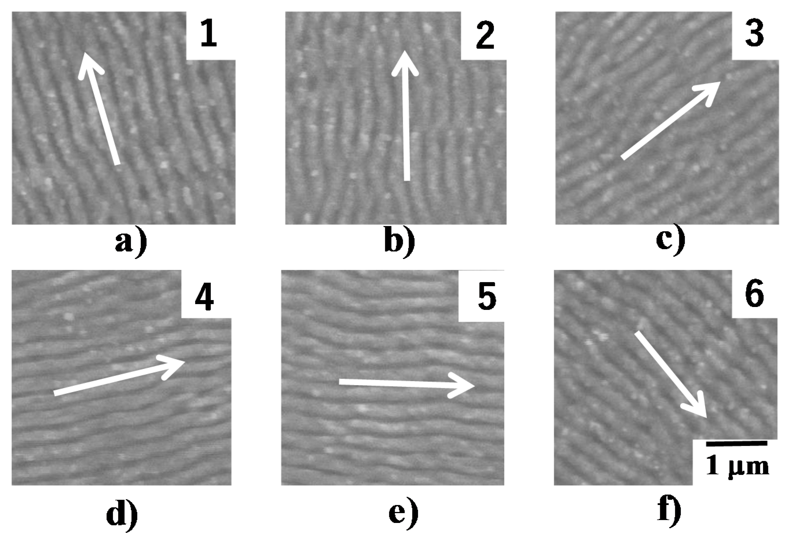
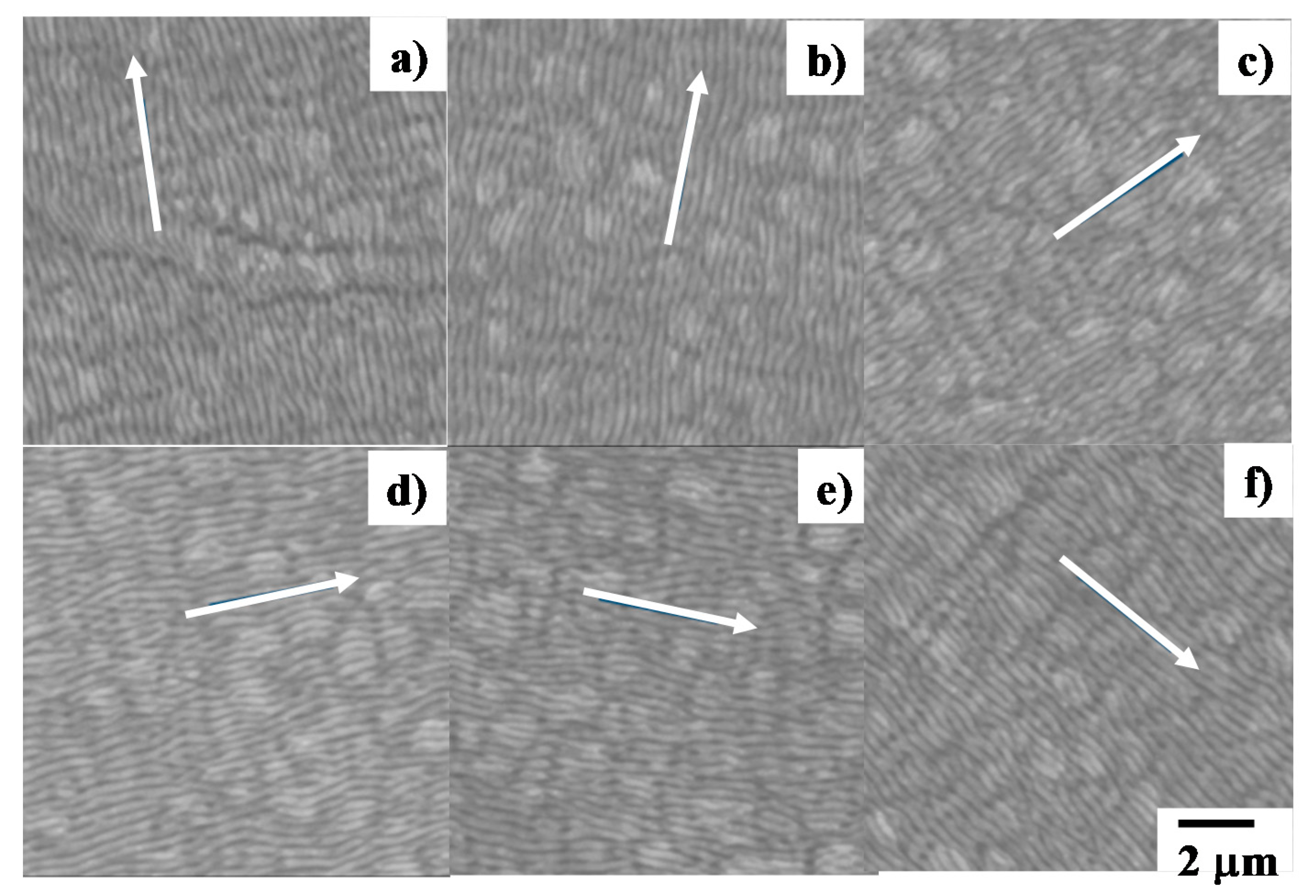
3.1. Formation of Unidirectional Nanotextures onto Stainless Steels

With use of the galvanometer, the laser beam path was controlled to form the unidirectional nanotextures onto the AISI304 stainless steel sheets on the X-Y stage by the present femtosecond laser processing. The laser beam was scanned in the specified angle (θ) by this galvanometer; this angle was incrementally rotated clockwise. In the case when the laser fluence was 0.6 J/cm2 and the wave length was 512 nm, the LIPSS ripple period was estimated to be 300 nm. Figure 2 depicts the six nanotextures formed onto the AISI304 sheet with a clockwise rotation of nanotexture orientation from 0° for Figure 2a to 180° for Figure 2f with an incremental angle of 30°.
The nanotextures in Figure 2a–f are aligned to the specified orientation in parallel to each other. Among Figure 2a–f, the nanotexture width remains to be constant by 300 nm. This directional controllability of nanotextures reveals that a two-dimensional segment is printed as a unidirectional assembly of nanotexture with the specified orientation and then every two-dimensional microtexture is designed and constructed by a patchwork of segments to have distributed nanotextures.
In order to demonstrate this possibility to form the patchworked microtexture by nanotextured segments, a two-dimensional matrix with 8 rows × 8 columns is designed to be built up by assembling the 8 × 8 (= 64) segments with six different nanotextures. Figure 3a represents how to distribute the unidirectional nanotextures for each segment; e.g., the nanotexture in Figure 2c is allocated to (1,1)-segment in the matrix by notation of No.3 while the nanotexture in Figure 2b, to (8,8)-segment by notation of No.2. Figure 3b shows the optical microscopy image on the patchworked microtexture. Each surface plasmonic color corresponds to each segment in the matrix.
If this collaring were induced by the grating techniques, the tone in collaring could be insensitive to the change of nanotexture orientations. As depicted in Figure 3b, the segments allocated with the same nanotextures in Figure 3a have a different tone in blue; e.g., the segment at (8,2) colors light blue but the segment at (8,8) colors darker blue even when the same nanotexture with Figure 2b is allocated to two segments in Figure 3a. This sensitiveness of tone in the blue range under normal lighting explains that this surface color decoration is induced by plasmonic brilliance on the nanotexture with the period of 300 nm.

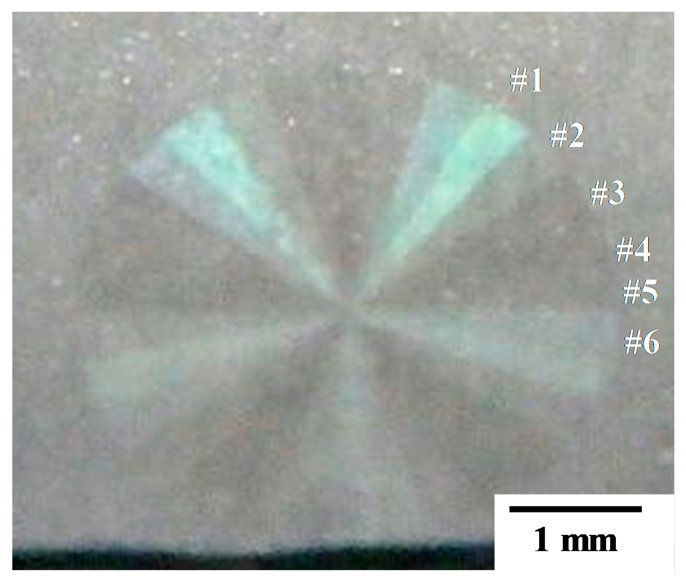
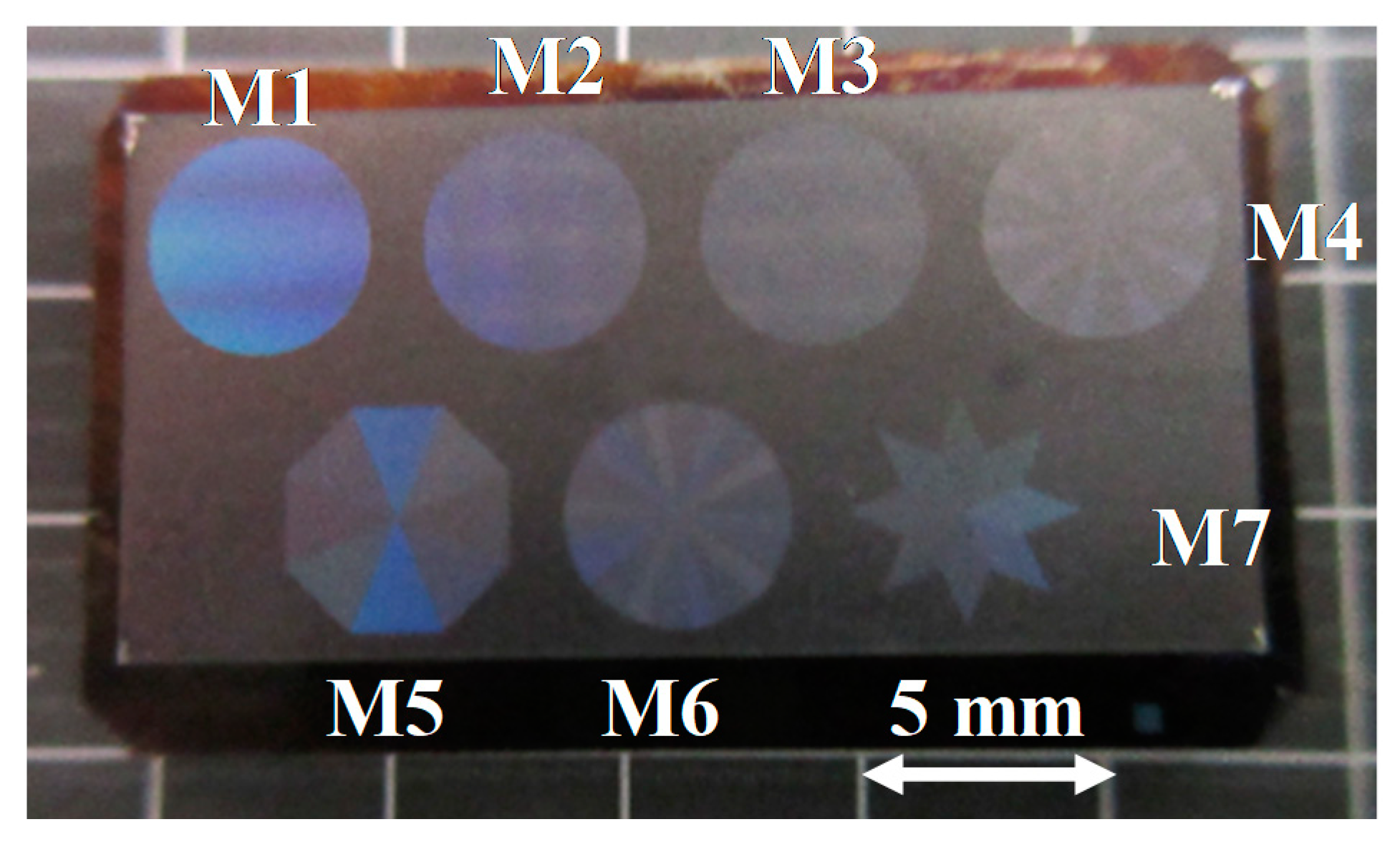
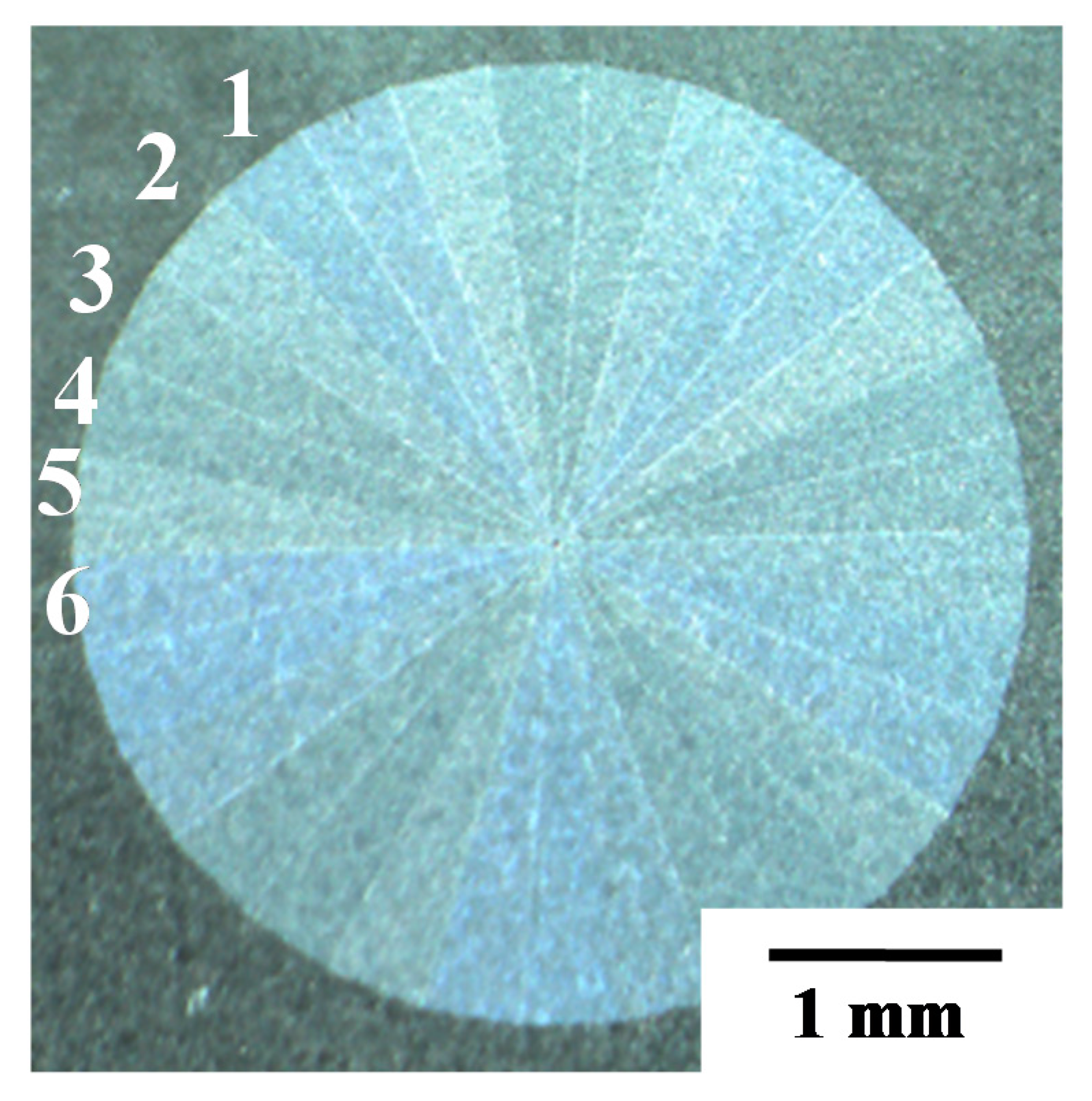
3.2. Fabrication of AISI316 Micro-/Nano-Textured Punch

The nitrided AISI316 substrate was micro-/nano- textured by the femtosecond laser processing to prepare for a punch for precise embossing. Figure 4 shows seven patterns (M1–M7) which are micro-textured onto the surface of nitrided AISI316 punch. They consist of three circular patterns (M1, M2, M3), three polygonal patterns (M4, M5, M6), and a star-shaped one (M7). As stated in [20,21], each micro-textured pattern is colored in dark blue by surface plasmonic brilliance in optics. Since the LIPSS-ripple period is around 300 nm in these nanotextures, this blue color range is selected in the optical diffraction to nanotextures.
This diffractive color is different in each segment of seven micropatterns in Figure 4, as suggested by coloring in the matrix in Figure 3. This reveals that allocation of nanotextured ripples with their tailored orientation to each segment controls the color tone of micropatterns for surface decoration. The M6 micropattern is employed to explain this controllability.
Figure 5 depicts the optical microscopic image on the polygonal micropattern, M6. This microtexture consists of five repetitive sections; each section is further divided into six segments from #1 to #6 in Figure 5 with different nanotextures. As stated in 3.1, each segment has different surface plasmonic brilliances with dependence on the orientation of nanotextures. Figure 6 lists the SEM images on the nanotextures allocated to six segments for five sections in the microtexture of M6 on the die. The orientation of nanotexture is controlled to rotate clockwise (a)–(f) in correspondence from segment #1 to #6 in Figure 5. Irrespective of this rotational control, the spatial period of six nanotextures is constant by 300 nm for all segments and sections in this microtexture of M6. Figure 5 and Figure 6 demonstrate that the microtextures of M6 is shaped as a regularly tailored assembly of nanotextures with their controlled orientations.
Each of the other six micropatterns in Figure 5 is also composed of geometrically designed assembly of sections, each section of which consists of segments with designated nanotextures as seen in Figure 5 and Figure 6. To be noticed in Figure 6, each nanotexture is continuous across the grain and zone boundaries of nitrided AISI316 punch. This proves that femtosecond laser processing works as a tool to print the original nanotextures onto the fine-grained and hardened AISI316 punch. This punch is used for precise coining onto the metallic products.

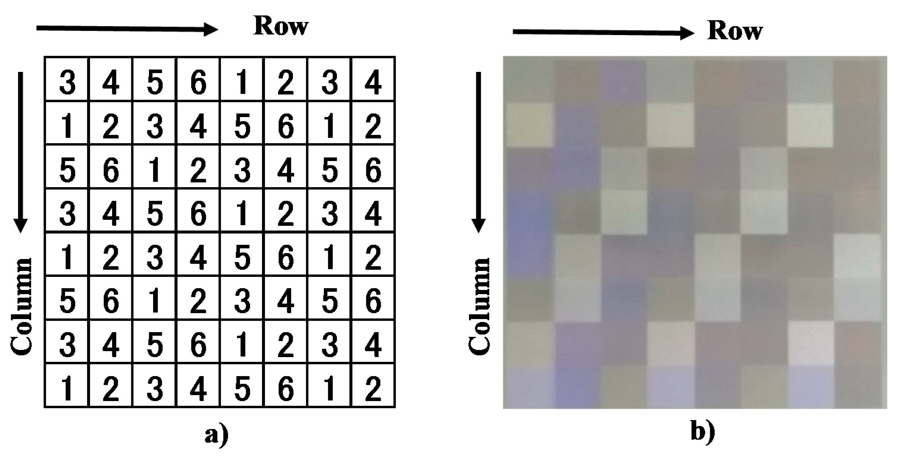
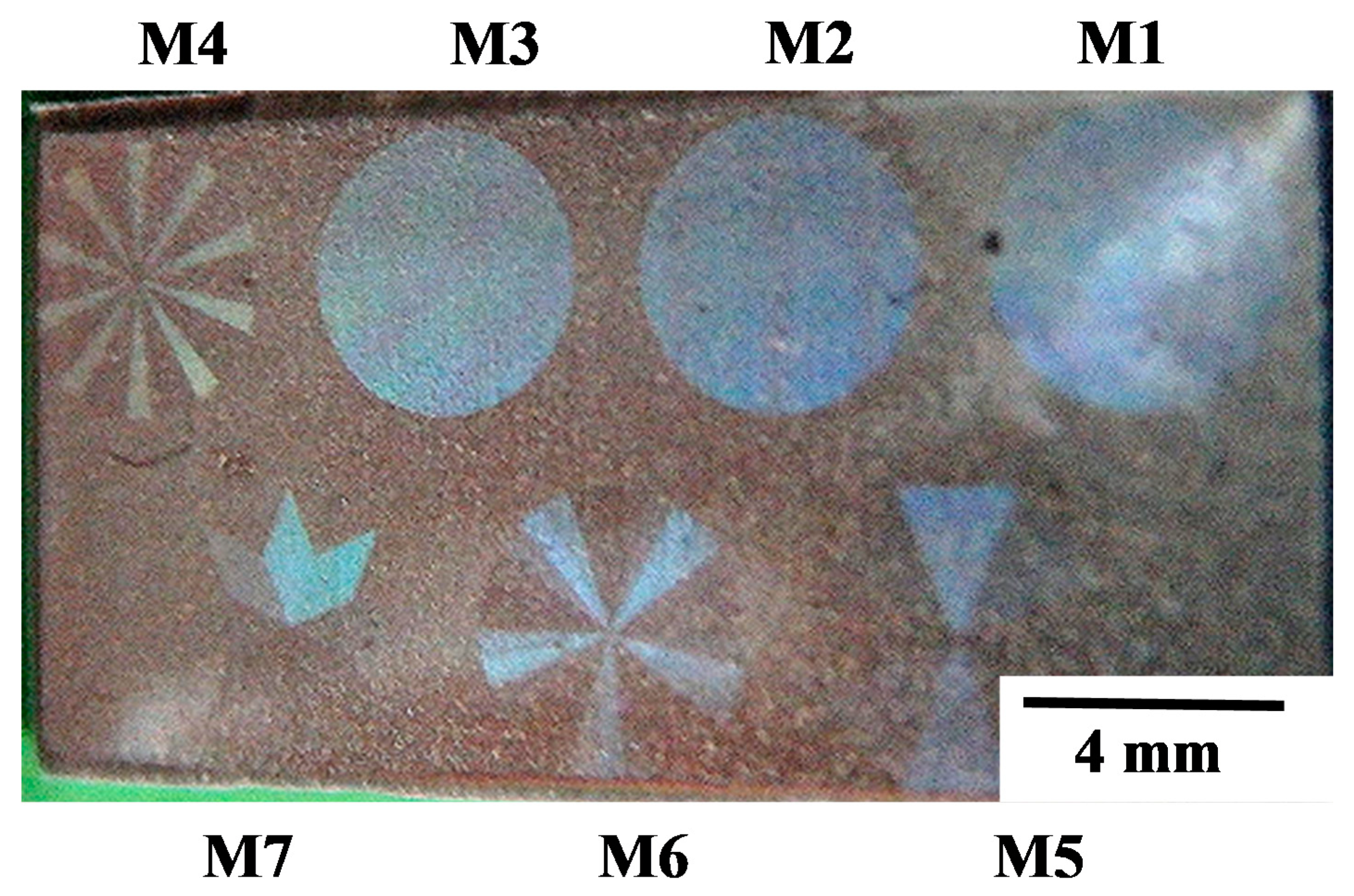
3.3. Coining of Micro-/Nano-Textures onto AA1060 Aluminum Plates

A single-mode loading sequence was used to compress the upper punch with the constant velocity. First, the punch was lowered from the original position down to the starting position, where the punch touched just on the work material surface. Then, the stroke was moved down to 150 μm from the starting position by the constant velocity of 0.02 mm/s. After holding this stroke for 10 s, the punch was moved up by the constant velocity of 0.1 mm/s. Figure 7 depicts the embossed AA1060 aluminium plate after single-shot loading in the above. This stroke of 150 μm is larger than the depths of microtextures and nanotextures in Figure 7. This is because the elastic deformation of AA1060 aluminum surface roughness is included in this total stroke together with the elastic response in the supporting jig of aluminum work. In addition, the depths of coined textures on the aluminum plate are not constant in the whole area during coining because of uneven distribution of coining pressure and elastic deformation of punch and die. In fact, the ratio of depth of coined textures on the aluminum plate to the height of textures on the punch was limited by 80%. The incremental loading sequence might be well employed to increase this ratio.
Seven microtextures from M1 to M7 are duplicated on the aluminum plate surface to have their surface plasmonic brilliance. Seven microtextures from M1 to M7 on the coined aluminum plate in Figure 7 are just corresponding in mirror image to seven micropatterns from M1 to M7 on the AISI316 punch in Figure 4. A micropattern of M6 is employed as a representative to describe the dimensional accuracy in this coining process by comparing Figure 5 and Figure 8. As stated, this M6 micropattern consists of five patch-works of six segments. The segments from #1 to #6 in Figure 5 are duplicated to #1 to #6 in Figure 8. Through coining, the anti-clock wise numbering of six segments in Figure 5 turns to be clockwise in Figure 8. This agreement between the original M6 micropattern and the coined M6 microtexture implies that each nanotexture in each segment is also accurately transcribed from the AISI316 punch to the aluminum work surface.
Figure 9 compares the nanopattern with LIPSS-ripples for segment #1 in micropattern M6 on the AISI316 punch to the nanotexture for segment #1 in microtexture M6 of the coined AA1060 aluminum plate. The average nanotexture period remains to be the same as the original LIPS-period of 300 nm. The original orientation angle (θ) in Figure 9a is −30° while θ = +30° in Figure 9b. This mirror-image reverse relationship proves that the original nanopattern on the punch is accurately transcribed to the aluminum plate.

4. Discussion

Micro-/nano-textures on the nitrided AISI316 die were coined onto the pure aluminum plate surfaces by the CNC stamping system with the stroke control. The dimensional accuracy in this coining process can be evaluated by two approaches. The high resolution SEM analysis works as the first method to prove that nanotextures with the LIPSS-period of 300 nm are precisely coined to the aluminum surface. As shown in Figure 9, the nanogroove texture with the orientation of −30° in segment #1 in the M6 micropattern on the punch is transcribed into the AA1060 aluminum plate surface with the same LIPPS period of 300 nm and the orientation of +30°. This mirror nanotexture reversal proves that each segment with an alignment of nanotextures and each microtexture with patchwork of segments can be also accurately transcribed into the aluminum plate surface. The surface plasmonic brilliance intrinsic to each nanotexture works as the second method to demonstrate that each segment and each microtexture can be coined with accuracy. Let us compare the original surface plasmonic brilliance to the micropattern M6 in Figure 5 with that in the coined microtexture M6 in Figure 8. As stated next, the color tone in each nanotexture is sensitive to positioning of the die and plate as well as lighting for observation. However, the variation of color tone from #1 to #6 in Figure 5 is transcribed to that from #1 to #6 in Figure 8.
The fundamental optics in this optical decoration is determined by surface plasmonic characteristics on the nanotextures with the specified LIPSS period (Λ) [22]. In the present laser nano-texturing, Λ = 300 nm; the wave length of the induced surface plasmon at these nanotextures ranges around 300 nm. That is, the color tone ranges from light blue to dark blue. As seen in Figure 3b, Figure 4, Figure 5, Figure 7, and Figure 8, every plasmonic brilliance on the die and AA1060 aluminum surfaces is characterized by the light to dark blue tone. As stated in Figure 3, this color tone is sensitive to the orientation of unidirectional nanotextures. When the specimen with coined micro-/nano-textures does not deform by the external stimulus, its surface disturbance on the surface is detected by the change in this surface plasmonic color tone.
Let us consider two types of stimulation to change the micro-/nano-textured specimen surface. When the liquid swells on a part of surface, the surface plasmon disappears on this local spot. As discussed in [18,19], every metallic material surface with micro-/nano-textures become hydrophobic and super-hydrophobic. Then, the surface plasmon disappears only on the hydrophobic spot while it remains the same as before on the other surface of textured surface. This reveals that the liquid deposition in a small volume can be detected by the change in the surface plasmonic pattern. Bacteria, virus or cell has a nature to deposit and swell on the material surface with specified nano-textures [23]. These solid deposits are detected by the selective disappearance of surface plasmon at the nanotextured segment with the designated LIPSS-period. The present laser-nanotexturing tool and coining process is also utilized to fabricate a metallic specimen by coining the tailored microtextures with aligned nanotextures even with the controlled LIPSS-period. Where the bacteria, the viruses, and the cells deposit on the coined metallic specimen is precisely detected by the local disappearance of surface plasmon.
The current attack by COVID19 teaches us that every man-made part and tool must be anti-bacterial not to make infection to a human being only by touching these parts and tools. Several papers insisted that nano-textured surface decoration by formation of a nanostructured oxide layer was effective to make the titanium part anti-bacterial and to control the bio-activeness of titanium surface by nanotexturing [24,25,26]. Their approach stood on the naturally grown oxide nanostructure; the present surface decoration has a potential to vary the spatial frequency, distribution, and orientation of nanotextures and to control the anti-bacterial surface condition of any material products.

5. Conclusions

The AISI316 substrate was plasma nitrided at 673 K for 14.4 ks as a mother die to be micro-/nano-textured by using the femtosecond laser processing. Seven micropatterns were machined onto this die; each microstructure was geometrically composed of several patchworks. Every patchwork also consisted of several nano-textured segments. This multi-dimensional design of micro-/nano-textures enables constructing various microstructures with the tailored nanotextures onto the mother die surface. In particular, the nanotexture period as well as its regular alignment and designable orientation are a key factor to make full use of the femtosecond laser surface decoration of dies. The preliminary plasma nitriding is useful to reduce the grain size of die material and to enhance its hardness and strength enough to be used in fine stamping for coining these micro-/nano-textures onto various metallic products.
CNC-stamping is useful to transcribe the original micropatterns and nanopatterns on the die to every metallic work material. The original patchwork of nanotextured segments in each micropattern on the punch surface is preserved and coined onto the work surface. Every patchwork as well as each segment is reproduced in the mirror-image reversal. As suggested in [15], this coining of micro-/nano-textures can be performed simultaneously with near-net shaping the metallic sheet and plate into parts and tools.
Surface plasmonic brilliance is a key factor in the present surface decoration. Since the nanotexture period in the present study is around 300 nm, its color tone ranges from light to dark blue. Each segment in every micropattern and microtexture is identified to have a different color tone by this surface plasmon. Every microtexture on the coined work products is composed of a nanotextured segment assembly; it has its intrinsic surface plasmon color tone. Any deposits and adheres on this product surface can be detected by local disappearance of this color tone. No change in this optical characteristic on the product surface proves that its surface is antibacterial in practice by the present surface decoration.

Author Contributions

Conceptualization, T.A. and T.I.; methodology, T.A.; formal analysis, T.A.; investigation, T.A. and T.Y.; data curation, T.I.; writing—original draft preparation, T.A.; writing—review and editing, T.A.; visualization, T.A. and T.Y.; funding acquisition, T.I. All authors have read and agreed to the published version of the manuscript.

Funding

This research received no external funding.

Acknowledgments

The authors would like to express their gratitude to Yasuyuki Okabe (LPS-Works, Co., Ltd.) and Shu-Ichi Kurozumi (Nano-Film Coat, LLC.) for their help in the experiments.

Conflicts of Interest

The authors declare no conflict of interest.

References

  1. GF Laser Texturing Revolution Dans la Decoration Horlogere. Available online: https://www.swissphotonics.net/libraries.files/nicolet.pdf (accessed on 8 July 2020).
  2. Yang, Y.; Pan, Y.; Guo, P. Structural coloration of metallic surfaces with micro/nano-structures induced by elliptical vibration texturing. Appl. Surf. Sci. 2017, 402, 400–409. [Google Scholar] [CrossRef]
  3. Aizawa, T.; Hasegawa, T.; Inohara, T. Surface geometry control of stainless steels by femtosecond laser nano-/micro-texturing toward super-hydrophilicity and super-hydrophobicity. In Proceedings of the 12th AFGS, Kunming, China, 12 August 2019; pp. 71–78. [Google Scholar]
  4. Aizawa, T.; Inohara, T.; Wasa, K. Femtosecond laser micro/nano-texturing of stainless steels for surface property control. Micromachines 2019, 10, 512. [Google Scholar] [CrossRef] [PubMed] [Green Version]
  5. Aizawa, T.; Inohara, T.; Wasa, K. Fabrication of hydrophobic stainless steel nozzle by femtosecond laser micro-/nan-texturing. Int. J. Automot. Technol. 2020, 14, 159–166. [Google Scholar] [CrossRef]
  6. Gong, L.; Zhao, J.; Huang, S. Numerical study on layout of micro-channel heat sink for thermal management of electric devices. Appl. Therm. Eng. 2015, 88, 480–490. [Google Scholar] [CrossRef]
  7. Aizawa, T.; Shiratori, T.; Wasa, K. Plasma-printed AISI316L multi-punch array for fabrication of aluminum heatsink with micro-pillar fines. In Proceedings of the 3rd WCMNM International Conference, Raleigh, NC, USA, 10–12 September 2019; pp. 220–223. [Google Scholar]
  8. Jung, S.M.; Preston, D.J.; Jung, H.Y.; Deng, Z.; Wang, E.N.; Kong, J. Porous Cu nanowire aerosponges from one-step assembly and their applications in heat dissipation. Adv. Mater. 2016, 28, 1413–1419. [Google Scholar] [CrossRef] [PubMed]
  9. Aizawa, T.; Wasa, K.; Tamagaki, H. A DLC-punch array to fabricate the micro-textured aluminum sheet for boiling heat transfer control. Micromechanics 2018, 9, 147. [Google Scholar] [CrossRef] [PubMed] [Green Version]
  10. Aizawa, T.; Ono, N. Boiling heat transfer control by micro-/nano-texturing of metallic heat-spreading devices. In Proceedings of the 4th WCMNM International Conference, Mumbai, India, 14 March 2021. In press. [Google Scholar]
  11. Misun, P.M.; Hierlemann, A.; Frey, O. Miniature fluidic microtissue culturing device for rapid biological detection. In Miniature Fluidic Devices for Rapid Biological Detection; Springer: New York, NY, USA, 2018; pp. 207–225. [Google Scholar]
  12. Browne, D.J.; Karakozian, S.; Chen, X. Cell Culturing Device. U.S. Patent US2015.0072377 A1, 12 March 2015. [Google Scholar]
  13. Su, Y.; Luo, C.; Zhang, Z.; Hermawan, H.; Zhu, S.; Huang, J.; Liang, Y.; Li, G.; Ren, L. Bioinspired surface functionalization of metallic biomaterials. J. Mech. Behav. Biomed. Mater. 2018, 77, 90–105. [Google Scholar] [CrossRef] [PubMed]
  14. Davim, P. Nontraditional Machining Processes: Research Advances; Springer: New York, NY, USA, 2013. [Google Scholar]
  15. Aizawa, T.; Inohara, T. Pico- and femtosecond laser micromachining for surface texturing. In Micromachining; InTech-Open: London, UK, 2019; pp. 1–24. [Google Scholar]
  16. Aizawa, T.; Shiratori, T.; Kira, Y.; Inohara, T. Simultaneous nano-texturing onto a CVD-diamond coated piercing punch with femtosecond laser trimming. Appl. Sci. 2020, 10, 2674. [Google Scholar] [CrossRef]
  17. Derrien, T.J.-Y.; Koter, R.; Kueger, J.; Hoem, S.; Rosenfeld, A.; Bonse, J. Plasmonic formation mechanism of periodic 100nm-structures in femtosecond laser irradiation of silicon in water. J. Appl. Phys. 2014, 116, 074902. [Google Scholar] [CrossRef]
  18. Hasegawa, T.; Aizawa, T.; Inohara, T.; Wasa, K.; Anzai, M. Hot mold stamping of optical plastics and glasses with transcription of super-hydrophobic surfaces. Procedia Manuf. 2019, 15, 1437–1444. [Google Scholar] [CrossRef]
  19. Hasegawa, T.; Aizawa, T.; Inohara, T.; Yoshihara, S.-I. Mold-stamping of optical glasses by micro/ nano-textured die to transcript the hydrophobicity. J. JSTP 2019, 60, 23–27. [Google Scholar] [CrossRef]
  20. Aizawa, T.; Inohara, T.; Wasa, K. Nano-texturing onto tool-surface by the femtosecond laser processing. In Proceedings of the 4th WCMNM 2020, Mumbai, India, 13 March 2021. In press. [Google Scholar]
  21. Vorobyev, A.Y.; Guo, C. Thermal response and optical absorptance of metals under femtosecond laser irradiation. Nat. Sci. 2011, 4, 488–495. [Google Scholar] [CrossRef] [Green Version]
  22. Shulka, P.; Waugh, D.G.; Lawrence, J.; Vilar, R. Laser surface structuring of ceramics, metals and polymers for biomedical applications: A review. In Laser Surface Modification of Biomaterials; Woodhead Publishing: Cambridge, UK, 2016; pp. 281–299. [Google Scholar]
  23. van Driel, H.M.; Sipe, J.E.; Young, J.F. Laser-induced periodic surface structure on solids: A universal phenomenon. Phys. Rev. Lett. 1982, 49, 1955–1958. [Google Scholar] [CrossRef]
  24. Jang, Y.; Choi, W.T.; Johnson, C.T.; Garcia, A.J.; Singh, P.M.; Breedveld, V.; Hess, D.W.; Champion, J.A. Inhibition of bacterial adhesion on nanotextured stainless steel 316L by electrochemical etching. ACS Biomater. Sci. Eng. 2018, 4, 90–97. [Google Scholar] [CrossRef] [Green Version]
  25. Ferraris, S.; Cochis, A.; Cazzola, M.; Tortello, M.; Scalia, A.; Spriano, S.; Rimondini, L. Cytocompatible and anti-bacterial adhesion nanotextured titanium oxide layer on titanium surfaces for dental and orthopedic implants. Front. Bioeng. Biotechnol. 2019, 9, 103–110. [Google Scholar] [CrossRef] [PubMed]
  26. Ferraris, S.; Vemturello Miola, M.; Cochis, A.; Rimondini, L.; Spriano, S. Antibacterial and bioactive nanostructure titanium surfaces for bone integration. Appl. Surf. Sci. 2014, 311, 279–291. [Google Scholar] [CrossRef]
Figure 1. Three step experimental procedures for the decorative coining process to duplicate the computer aided design (CAD) data of micropatterns with nanotextures onto the metallic plate. (a) Plasma nitriding for fabrication of the die substrate, (b) femtosecond laser texturing onto the die substrate, and (c) computer numerical control (CNC)-stamping for precise coining of micro-/nano-textures to metallic plates.
Metals 10 01044 g001
Figure 2. Six nanotextures formed onto the stainless steel plates by the optical path control. Directivity of the nanotextures is controlled to rotate from (af). In the following, each nanotextured segment with the specified orientation was identified by each number; e.g., a nanotextured segment in Figure 2a was identified by No. 1.
Metals 10 01044 g002
Figure 3. Construction of two-dimensional microtextures as the 8 × 8 matrix of 64 segments with different nanotextures allocated to each one. (a) Allocation of nanotextures from “1” in Figure 2a to “6” in Figure 2f to each segment with (i,j) for 1 < i, j < 8 of matrix, and (b) surface plasmonic brilliant decoration of stainless steel plate surface on the matrix.
Metals 10 01044 g003
Figure 4. Seven microtexture patterns directly printed onto the nitrided AISI316 die surface.
Metals 10 01044 g004
Figure 5. Allocation of nanotextures with different orientations into six segments (#1–#6) in the M6 micropattern.
Metals 10 01044 g005
Figure 6. Nanotextures of six segments in M6 with a clockwise rotation of their orientations (af) in correspondence of #1 to #6 in Figure 5 by the femtosecond laser texturing.
Metals 10 01044 g006
Figure 7. Pure aluminum plate with coined seven microtextures, each of which has nanotextured segments. Each microtexture M1M7 in the above just corresponds to the original one from M1 to M7 in Figure 4.
Metals 10 01044 g007
Figure 8. Optical microscopic image on the microtexture of M6, coined onto the surface AA1060 plate. The coined segments are aligned in the clockwise numbering in the mirror-image reversal to the original anti-clockwise alignment in Figure 5.
Metals 10 01044 g008
Figure 9. Comparison of the nanotextures of segment #1 in the microtexture of M6 between the punch and the coined AA1060 specimen. (a) Nanopattern of #1 on M6 of the AISI316 punch, and (b) nanotexture of #1 on the M6 of coined AA1060.
Metals 10 01044 g009

