Article

Electrical and Mechanical Analysis of Different TSV Geometries

1
School of Engineering, Faculty of Science and Engineering, University of Wolverhampton, Wolverhampton TF2 9NN, UK
2
Department of Materials Science and Engineering University of Seoul, Seoul 130-743, Korea
*
Author to whom correspondence should be addressed.
Metals 2020, 10(4), 467; https://doi.org/10.3390/met10040467
Submission received: 21 February 2020 / Revised: 27 March 2020 / Accepted: 31 March 2020 / Published: 2 April 2020

Abstract

:
Through-silicon via (TSV) is an important component for implementing 3-D packages and 3-D integrated circuits as the TSV technology allows stacked silicon chips to interconnect through direct contact to help facilitate high-speed signal processing. By facilitating the stacking of silicon chips, the TSV technology also helps to meet the increasing demand for high density and high performance miniaturized electronic products. Our review of the literature shows that very few studies have reported on the impact of TSV bump geometry on the electrical and mechanical characteristics of the TSV. This paper reports on the investigation of different TSV geometries with the focus on identifying the ideal shapes for improved electrical signal transmission as well as for improved mechanical reliability. The cylindrical, quadrangular (square), elliptical, and triangular shapes were investigated in our study and our results showed that the quadrangular shape had the best electrical performance due to good characteristic impedance. Our results also showed that the quadrangular and cylindrical shapes provided improved mechanical reliability as these two shapes lead to high Cu protrusion of TSV after the annealing process.

Graphical Abstract

1. Introduction

The increasing demand for lower cost, miniaturized, and multi-functional electronic devices with lower power consumption has given rise to a number of new manufacturing challenges. To meet these challenges, the electronics packaging R&D industry has worked hard in recent years to develop novel interconnection materials, process techniques, and packaging technologies such as the through-silicon via (TSV) technologies [1,2].
TSV is becoming a promising solution that can offer the shortest interconnection, minimum chip-to-chip bonding pad sizes and spacing, and can greatly improve the density of integration and performance. Additionally, it can provide novel packaging applications for delivering the highest level of silicon integration and space efficiency at the lowest cost [3,4,5].
The TSV manufacturing process includes via formation, filling, annealing, and wafer thinning. In general, Cu (copper) is the most widely used material for filling the TSV, and forms the electrical connection between the active side to the backside of the silicon die. High conductivity, low cost, and good compatibility with the multilayer interconnects process are the main merits of using copper as the filler material in the TSV [6].
Although the use of TSV can provide several benefits in implementing 3D packaging and 3D integrated circuits, the TSV fabrication and manufacturing processes have been associated with a number of electrical and mechanical reliability issues and challenges [7].
One of the main electrical reliability issues that have been linked with TSV fabrication and manufacturing processes is the signal degradation due to crosstalk and other switch noises. As TSVs are mostly used for signal and power transmission, TSVs used in high frequency applications tend to be affected by crosstalk signal distortion. Equally, the main mechanical reliability challenge is the formation of Cu protrusion caused by the TSV manufacturing process, which is known to induce high stress levels in the wafer [7,8,9]. Indeed, because of the large coefficient of thermal expansion (CTE) mismatch between Cu (l6.7 ppm/°C) and silicon (2.3 ppm/°C), the material surrounding the TSV (silicon) can experience several reliability issues such as chip or wafer warpage, interfacial delamination, and cracking. This paper reports on the investigation of different TSV geometries with the focus on identifying the ideal shapes for improved electrical signal transmission as well as for improved mechanical reliability.

2. Electrical Investigation of Through-Silicon Via (TSV) Structures

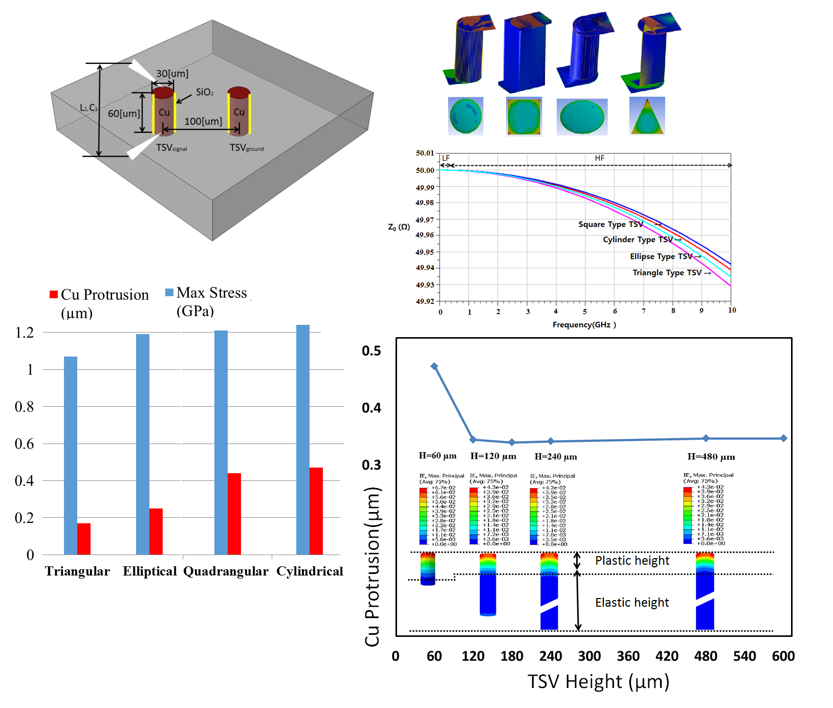
2.1. Through-Silicon Via (TSV) Structure and Manufacturing Process

The main steps used in TSV fabrication are via-drilling, dielectric barrier deposition, seed layer deposition, Cu-filling by electroplating, and chemical-mechanical polishing (CMP) [10]. The deep reactive ion etching (DRIE) process is used for via-drilling, and the process conditions used are 300 sccm SF6, 200 sccm, C4F8, 400 mtorr pressure, and 250 W RF power. For dielectric barrier deposition, the plasma enhanced chemical vapor deposition (PECVD) is used to make a SiO2 dielectric barrier to isolate Cu and Si. For seed layer deposition, a high density plasma chemical vapor deposition (HDP CVD) is used to form 0.3 μm Ti and 0.5 μm Cu layers, and they are deposited as seed layers on the dielectric barrier. The electroplating solution for Cu filling is prepared from 100 g CuSO4, 30 mL/L H2SO4, and small doses of additive. Plating is performed by applying a periodic pulse reverse (PPR) current. Finally, the Cu-filled silicon wafer is thinned to 60 μm using CMP. The steps described above were used for preparing a 4-inch wafer, consisting of 192 TSVs with 30 μm diameter, and 60 μm height that was used for testing (see Figure 1).
Electrical parameters such as inductance, L1, and capacitance, C1 were measured by a commercial tester of the Agilent Precision LRC meter (model: E4980A, Keysight Technologies Inc., Santa Rosa, CA, USA) in the frequency range of 1 Hz to 1 MHz before implementing the thermal shock test. The thermal shock test was performed to simulate the thermo-mechanical response according to the MIL-STD-833A standard. The temperature range was considered to be between −65 °C and 150 °C (with the dwell and ramp times set to 60 s). Samples were taken at 0, 500, and 1000 cycles. After the thermal shock test, the TSV cross-sections were analyzed by field emission-scanning electron microscopy (FE-SEM).

2.2. Electrical Simulation

The Advanced Design System (ADS), a commercial software, was used for the electrical simulation, and the adaptive sampling frequency (ASF) method was used for the analysis. To simplify the calculation, the dielectric load was ignored due to its small values. For more accurate simulation, the number of mesh and the curved angle were considered as 52 and 45°, respectively. TVS is a very small structure and needs very expensive processing to make the various TVS features. Thus, after manufacturing a single TSV, the characteristic values of the manufactured TSV and the simulated TSV were compared and analyzed. Based on this, various structures of TSVs were analyzed using only the simulation. At low-bandwidth frequencies (1~100 MHz, see Figure 2), the measurements and simulations were performed and compared; at high-bandwidth frequencies (1~10 GHz, see Figure 3 and Figure 5), only simulations were performed because the measurement is difficult.
Characteristic impedance (Z0), which is the ratio of the amplitudes of voltage and current of a single wave propagating along the line, is a measure of how effectively the signal is delivered through a transmission line. Z0 can be expressed by Equation (1), where R is resistance, L is inductance, G is conductance, C is capacitance, j is imaginary unit, and ω is the angular frequency.
Z 0 = R + j ω L G + j ω C
Figure 2 shows that for frequencies in range of 1~100 MHz, Z0 was measured at 48.5 Ω, whilst the Z0 value from the ADS simulator was 50.0 Ω (there was a difference of 3% between the measured and simulation values). This difference is due to the fact that the Cu material is assumed as a perfect conductor for the simulation and does not consider the errors that are associated with the TSV manufacturing process, whilst the real Cu material in the fabrication process may have some defects such as micro cracks caused by CMP process after Cu-filling.
The equivalent circuit for the TSV is composed of series inductance (L1), resistance (R1), shunt capacitance (C1), and conductance (G1). To calculate the electrical parameters, the measured S parameters are converted to the Z parameters by using Equation (2) and then the electrical parameters can be calculated from Equation (3) [11]. The Z parameter is a factor by which input voltage and current, and output voltage and current of the two-port network are related. For any two-port network, input voltage V1 and output voltage V2 can be expressed in terms of input current I1 and output current I2. Therefore, the Z parameter is defined as Z11 = V1/I1(I2 = 0), Z21 = V2/I1(I2 = 0), Z12 = V1/I2(I1 = 0), Z22 = V2/I2(I1 = 0) [11]. Here, the measured result for L1 and C1 were 0.052 nH and 0.022 pF, respectively. In addition, from the simulated S parameters, the calculated values of L1 and C1 were 0.063 nH and 0.030 pF, respectively.
[ Z 11 Z 12 Z 21 Z 22 ] = [ Z 0 ( 1 + S 11 ) ( 1 S 22 ) + S 12 S 21 ( 1 S 11 ) ( 1 S 22 ) S 12 S 21 Z 0 2 S 12 ( 1 S 11 ) ( 1 S 22 ) S 12 S 21 Z 0 2 S 21 ( 1 S 11 ) ( 1 S 22 ) S 12 S 21 Z 0 ( 1 S 11 ) ( 1 + S 22 ) + S 12 S 21 ( 1 S 11 ) ( 1 S 22 ) S 12 S 21 ]
L 1 = Imag ( Z 11 ( Z 12 + Z 21 ) ) 2 π f   ,         C 1 = Imag ( 2 Z 12 + Z 21 ) 2 π f

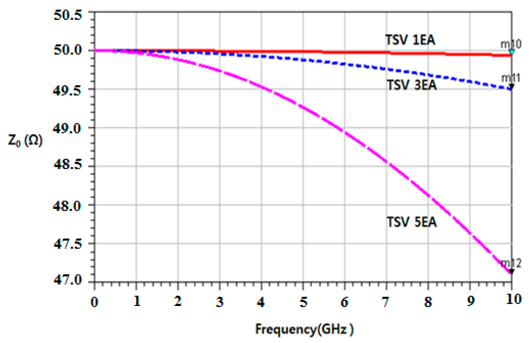
2.3. Characteristic Impedance of Multilayer TSV

TSVs are increasingly used in 3D packaging applications as they have the capacity to significantly speed up communication between layered chips, when compared to a planar layout. In this study, we considered the simulation of the characteristic impedance (Z0) of 1EA, 3EA, and 5EA multilayers in the frequency range of 1~10 GHz. Figure 3 shows the Z0 for different TSV layers (same Cu filled geometry in each layer) and it was assumed that Z0 for all multilayers was 50 Ω.
As can be seen, more multiple layers give higher Z0 values, because the increase in the total TSV length results in more parasitic inductance, which affects signal attenuation and increases the characteristic impedance.

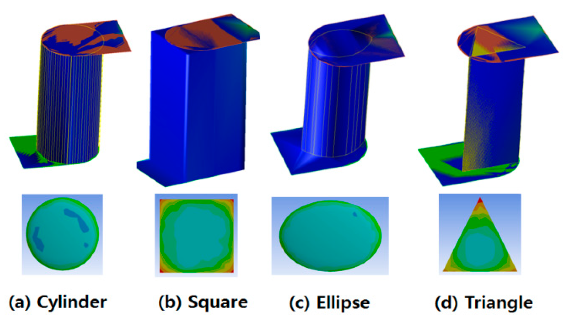
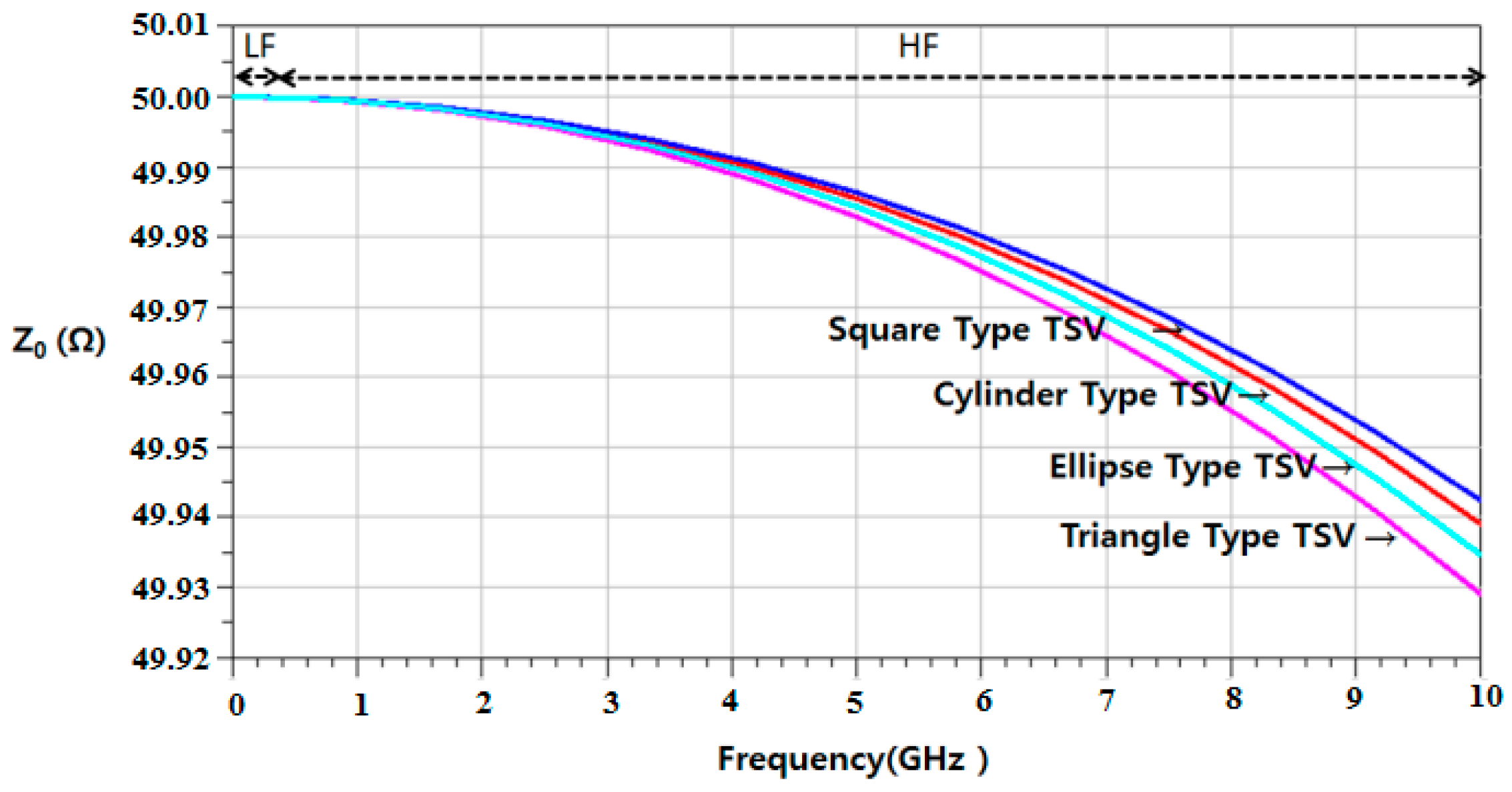
2.4. Characteristic Impedance for Different TSV Shapes

Figure 4 shows the cylindrical, quadrangular, elliptical, and triangular TSV shapes that were considered for the investigation of the characteristic impedance for different TSV shapes.
Equations (4) and (5) show that the skin effect (δ) is decreased by increasing the frequency; however, this leads to an increase in the effective resistance. This means that the AC current density (J) in a conductor decreases exponentially from its value at the surface (JS), according to the depth (d) from the surface, where ρ is resistivity, ω is angular frequency, μ is permeability, and ε is permittivity [12,13,14]. It should also be realized that the effective resistance causes a reduction in Z0.
J = J S e ( 1 + j ) d / δ
δ = 2 ρ ω μ 1 + ( ρ ω ϵ ) 2 + ρ ω ϵ
Figure 5 shows the characteristic Impedance for single TSV layers with different shapes in the frequency range between 1 and 10 GHz. As can be noted, in the low frequency (LF), there is no difference in Z0 for different TSV shapes, however, in high frequency (HF), the quadrangular (square) TSV shape had better electrical performance compared to the other shapes. This is because the quadrangular TSV shape has a higher insulating layer due to its large outer area and hence protects the signal more than other shapes. It should be noted that in case of multilayer TSVs, the effect of signal attenuation will further deteriorate the characteristic impedance (will lead to more reduction).

3. Mechanical Investigation of TSV Structures

One of the main reliability issues associated with the TSV fabrication process is the protrusion of Cu due to the Cu–Si CTE mismatch. Figure 6 shows the cross section of the Cu-filled TSV after 500 and 1000 cycles of the thermal shock test. After 1000 cycles, voids and cracks due to electro migration and protrusion (resulting from stresses induced by CTE mismatch) were found on the opening side and the wall side of the TSV. To reduce the effect of protrusion and improve the mechanical reliability of TSV, the annealing process is an effective approach that can be done in the fabrication process.

3.1. Finite Element Simulation (FEM)

ABAQUS 6.14 software was used for investigating the Cu protrusion of TSV that results during the annealing process for each of the TSV geometries. This finite element simulation (FEM) software was selected for its features in accurately investigating the nonlinearities in the geometry and material properties. Two symmetrical boundary conditions were applied to the FE models (only one symmetric plane in case of triangular shape). Three-dimensional continuum elements “C3D8R” with a fine mesh density in the Cu region were used to provide enough convergence in the results. As maximum protrusion appears at the maximum temperature, which is independent of the dwell time, therefore, dwell time was not taken into account. In addition, cooling time was not considered because of reduced protrusion during cooling. The annealing temperature used in the simulation was between 250 °C and 450 °C, while the temperature ramp rate was 5 °C/min [15]. Additionally, the temperature and time dependency of the materials (such as creep behavior) were not considered in this work. However, to find the Cu protrusion, plastic behavior (non-reversible deformation) was considered during rising temperatures. Table 1 shows the mechanical properties of the used materials in the simulation (Cu and Si) [15].

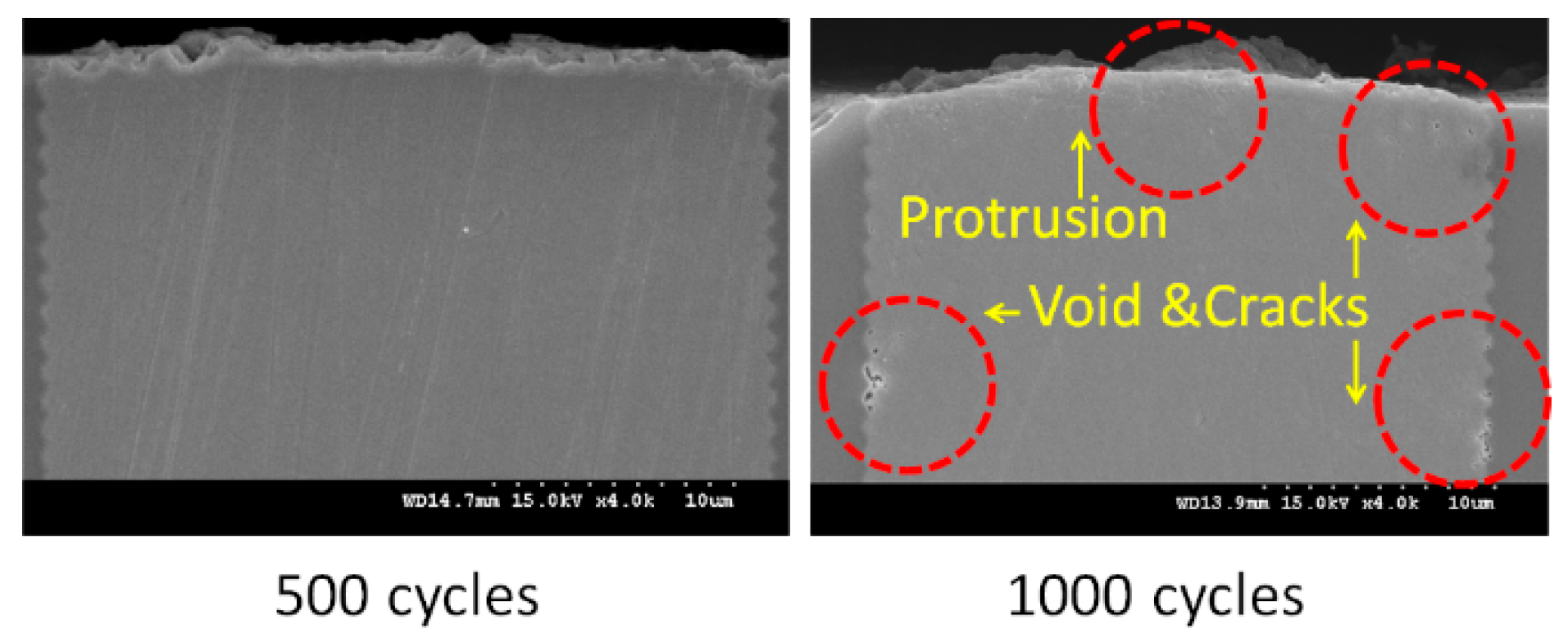
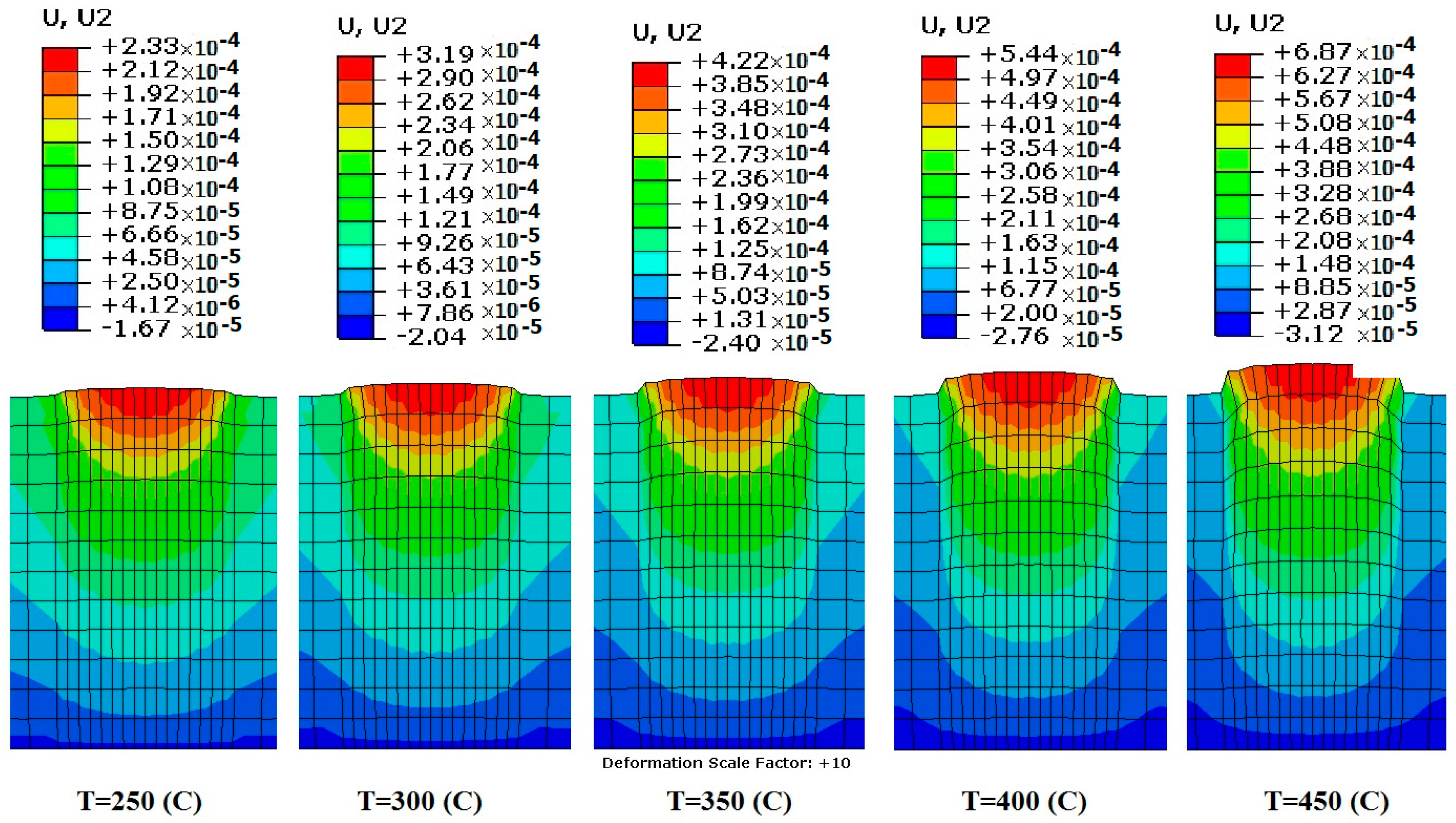
3.2. Protrusion on Single Layer TSV

Figure 7 displays the vertical deformation of the mid cross section of the cylindrical Cu filled TSV for temperatures between 250 °C and 450 °C. This FEM result showed that a greater annealing temperature induces further thermal expansion on the TSV.

3.3. Protrusion on Multilayer TSVs

Figure 8 shows the Cu protrusion for the 1EA, 3EA, and 5EA multilayer TSV under annealing temperatures from simulation. The diameter and height of each TSV layer were considered as 30 µm and 60 µm, respectively. From the results, the protrusion height of 1EA (single layer), 3EA, and 5EA were found to be 0.47 µm, 0.36 µm, and 0.35 µm, respectively, at 450 °C. For multilayer TSVs, the protrusion height was saturated because the top layers tended to expand in two sides of the vertical direction and the bottom surface of each layer compressed the top surface of bottom layer. Indeed, in the bottom layers, the upward thermal expansion was limited by downward expansion of its top layer. However, in the single layer, the top surface was completely free to expand, and hence the protrusion was higher than that of the multi-layer. The results showed that multilayer TSVs have less reliability as they have less Cu protrusion, and they also have a higher probability for cracks due to high stress level induced by the interaction between multilayers that are in contact.

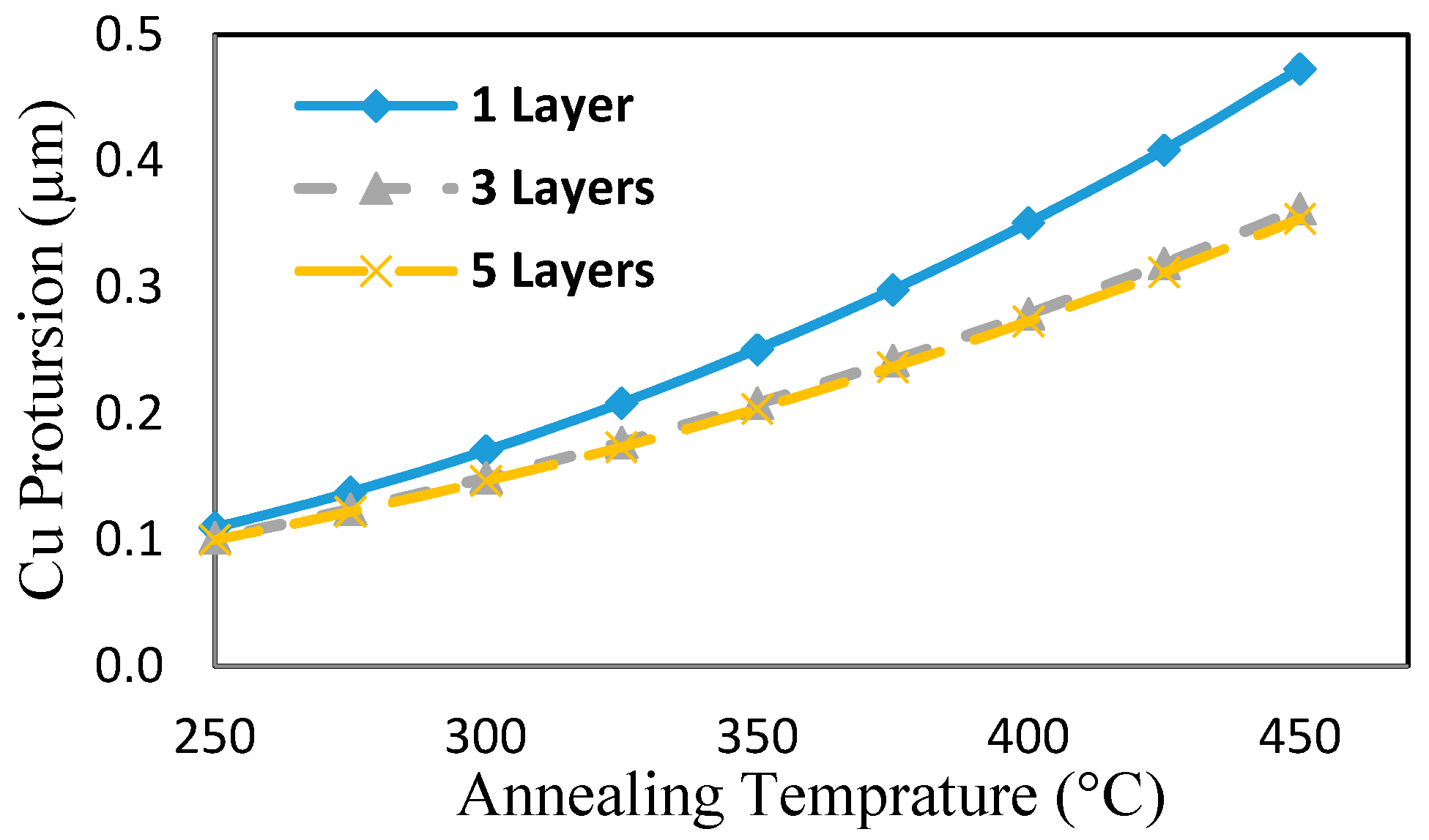
3.4. Effect of TSV Height on the Protrusion

The results for Cu protrusion of different cylindrical TSV height (from 60 µm to 600 µm) with a 30 µm diameter are shown in Figure 9. This figure shows that at 450 °C annealing, the protrusion height of 60 µm TSV was 0.47 µm, but decreased to about 0.33 µm for TSVs taller than 120 µm. During the high temperature annealing process, the Cu surface goes into plastic phase and plastic behavior can directly affect the expansion of Cu. As can be noted in Figure 9, by increasing the height of the TSV from 60 µm to values higher than 120 µm, the magnitude and height of the plastic region decrease from 45 µm to 40 µm. Indeed, the plastic height of TSV determines the extent of protrusion (plastic height of TSV is more important TSV height; higher plastic height leads to higher protrusion).

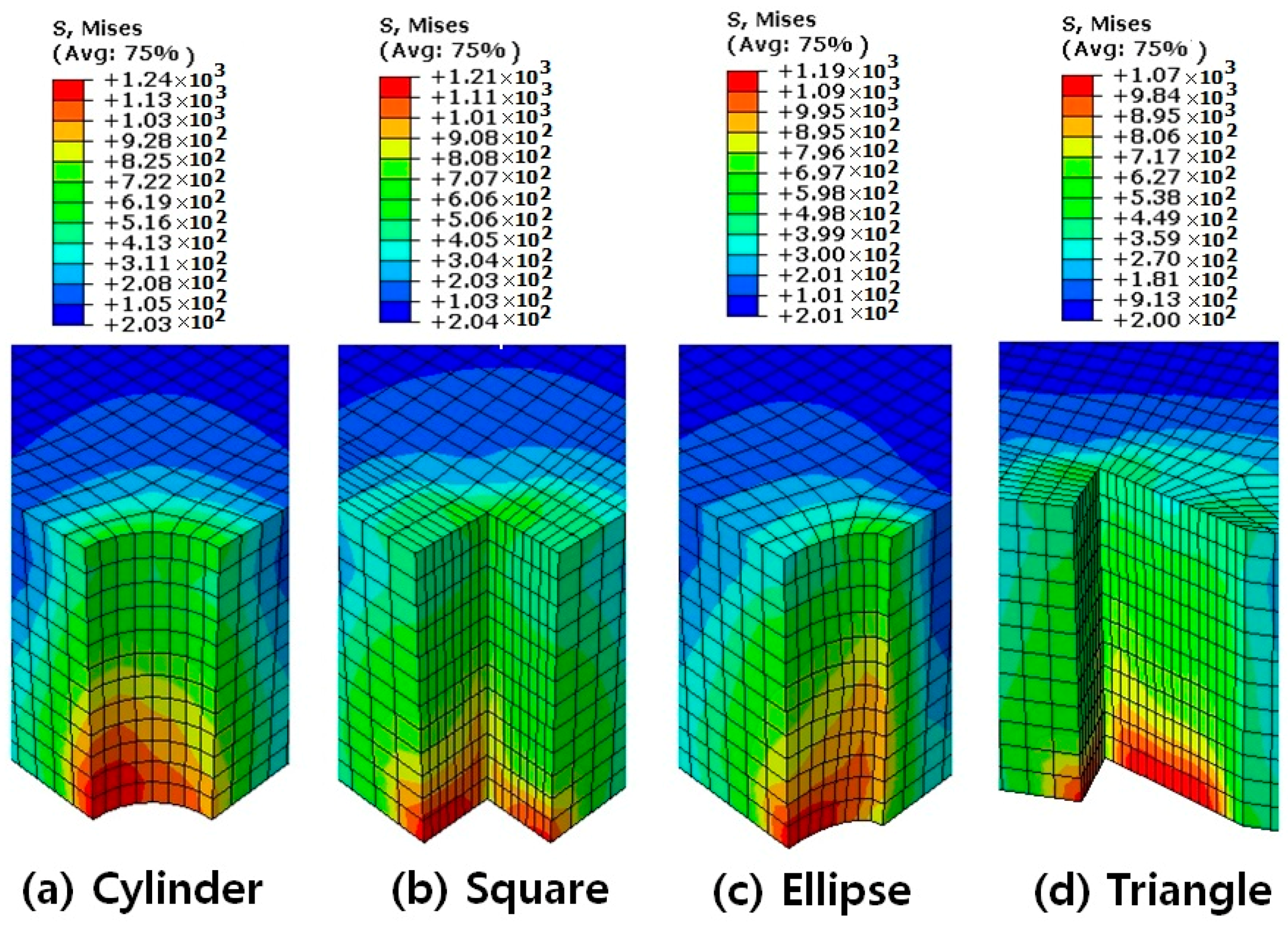
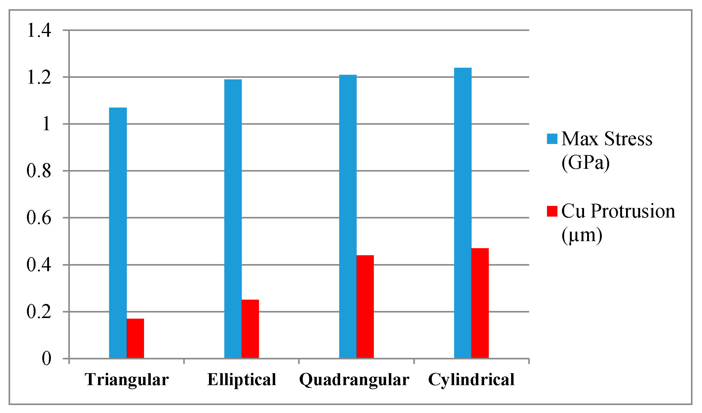
3.5. The Protrusion and Stress Analysis for Different TSV Shapes

Figure 10 displays the Von-Mises stress distribution in Si material for different TSV shapes at the 450 °C annealing temperature. For all TSV shapes, the maximum Von-Mises stress was concentrated on the bottom of the TSV and as can be noted, they had almost the same magnitude and distribution of stress (the maximum stress range was between 1.07 GPa and 1.24 GPa).
Figure 11 compares the Cu protrusion and maximum Von-Mises stress in Si for different TSV shapes after the 450 °C annealing process. As can be seen, the Cu protrusion of cylindrical, quadrangular, elliptical, and triangular shapes was 0.47 µm, 0.44 µm, 0.25 µm, and 0.17 µm, respectively. If we assume no differences in silicon stress levels for the different TSV shapes, then the cylindrical and quadrangular TSV shapes are more mechanically reliable due to reaching a higher Cu protrusion. It follows that the annealing process releases the internal stresses and causes Cu protrusion at the entrance of the TSV. The high Cu protrusion means that the internal stresses of the TSV have been released more and can suggest more reliability. The final TSV produced by the annealing process followed by the CMP process used for removing the CU protrusion led to a lower internal stress level.

4. Conclusions

This paper reports on the investigation of different TSV geometries with the focus on identifying the ideal shapes for improved electrical signal transmission and improved mechanical reliability. The cylindrical, quadrangular (square), elliptical, and triangular shapes were investigated in our study and our results showed that the characteristic impedance (Z0) for all multilayers investigated were about the same. The single layer TSV showed a higher Cu protrusion (due to reaching higher plastic height); increasing the number of layers did not lead to any significant change in the Cu protrusion height. However, the TSV Cu protrusion decreased for 60 µm to a 120 µm TSV height, and then remained constant for taller TSVs. In terms of TSV shape, the cylindrical and quadrangular TSV shapes showed improved mechanical reliability when compared with the elliptical and triangular shapes. Our results also showed that in low frequencies (less than 1 GHz), Z0 is constant for different TSV shapes, but in high frequencies, the quadrangular TSV shape showed improved electrical performance (due to having a higher insulating layer and better protecting the signal).

Author Contributions

I.H.J., performed the experiments, measurements and developed the first draft of the paper. A.E.M. undertook FEM simulations and results. J.P.J. and N.N.E. supervised the work and contributed to developing the outline of the paper. All co-authors contributed to the response of reviewers’ comments and have read and agreed to the final published version of the manuscript. All authors have read and agreed to the published version of the manuscript.

Funding

This research received no external funding and Alireza Eslami Majd’s Ph.D. Studies is funded by Faculty of Science and Engineering, University of Wolverhampton under their PGR Scholarships and Bursary Scheme.

Acknowledgments

The authors would like to acknowledge the support of the Faculty of Science and Engineering, University of Wolverhampton for providing the sponsorship for the corresponding author’s Ph.D. studies.

Conflicts of Interest

The authors declare no conflicts of interest.

References

  1. Kong, L.W. Visualization of extrusion and voids induced in TSV. Microelectron. Reliab. 2012, 92, 24–28. [Google Scholar] [CrossRef]
  2. Ding, Y.; Yan, Y.; Chen, Q.; Wang, S.; Su, R.; Dang, H. Analytical solution on interfacial reliability of 3-D through-silicon-via (TSV) containing dielectric liner. Microelectron. Reliab. 2014, 54, 1384–1391. [Google Scholar] [CrossRef]
  3. Choi, H.S.; Seo, W.S.; Choi, D.K. Prediction of reliability on thermoelectric module through accelerated life test and Physics-of-failure. Electron. Mater. Lett. 2011, 7, 271. [Google Scholar] [CrossRef]
  4. Kang, U.S.; Chung, H.J.; Heo, S.M.; Park, D.H.; Lee, H.; Kim, J.H.; Ahn, A.H.; Cha, S.H.; Ahn, J.; Kwon, D.M.; et al. 8 Gb 3-D DDR3 DRAM using through-silicon-via technology. IEEE J. Solid-state Circuit Conf. 2010, 45, 111–119. [Google Scholar] [CrossRef]
  5. Kumar, S.; Park, J.Y.; Jung, J.P. Analysis of high speed shear characteristics of Sn-Ag-Cu solder joints. Electron. Mater. Lett. 2011, 7, 365. [Google Scholar] [CrossRef]
  6. Roh, M.H.; Sharma, A.; Lee, J.H.; Jung, J.P. Extrusion Suppression of TSV Filling Metal by Cu-W Electroplating for Three-Dimensional Microelectronic Packaging. Metall. Mater. Trans. A 2015, 46, 2051–2062. [Google Scholar] [CrossRef]
  7. Lau, J.H. Overview and Outlook of Three-Dimensional Integrated Circuit Packaging, Three-Dimensional Si Integration, and Three-Dimensional Integrated Circuit Integration. ASME J. Electron. Packag. 2014, 136, 040801. [Google Scholar] [CrossRef] [Green Version]
  8. De Messemaeker, O.; Pedreira, V.; Vandevelde, B.; Philipsen, H.; De Wolf, I.; Beyne, E.; Croes, K. Impact of post-plating anneal and throughsilicon via dimensions on Cu pumping. In Proceedings of the 2013 IEEE 63rd Electronic Components and Technology Conference (ECTC), Las Vegas, NV, USA, 28–31 May 2013; pp. 586–591. [Google Scholar]
  9. Jeong, I.H.; Jung, D.H.; Shin, K.S.; Shin, D.S.; Jung, J.P. Electrical characteristics and thermal shock properties of Cu-filled TSV prepared by laser drilling. Electron. Mater. Lett. 2013, 9, 389–392. [Google Scholar] [CrossRef]
  10. Seo, S.W.; Park, J.H.; Seo, M.S.; Kim, G.S. The electrical, mechanical properties of through-silicon-via insulation layer for 3D ICs. In Proceeding of the Electronics Packaging Technology & High Density Packaging International Conference, Beijing, China, 10–13 August 2009; p. 64. [Google Scholar]
  11. Lu, J.Q.; Xu, Z. Through-silicon-via fabrication technologies, passives extraction, and electrical modeling for 3-D integration/packaging. Semicond. Manuf. IEEE 2013, 26, 23. [Google Scholar]
  12. Hayt, W.H. Engineering Electromagnetics, 5th ed.; McGraw-Hill: New York, NY, USA, 1989; ISBN 0070274061. [Google Scholar]
  13. Vander Vorst, A.; Rosen, A.; Kotsuka, Y. RF/Microwave Interaction with Biological Tissues; John Wiley and Sons, Inc.: Hoboken, NJ, USA, 2006; ISBN 978-0-471-73277-8. [Google Scholar]
  14. Jordan, E.C. Electromagnetic Waves and Radiating Systems; Prentice Hall: Upper Saddle River, NJ, USA, 1968; p. 130. ISBN 978-0-13-249995-8. [Google Scholar]
  15. Jing, X.; Lee, U.-H.; Xu, C.; Niu, Z.; Hao, H.; Bae, J.-Y.; Won, J.; Zhang, W. Effect of pre-CMP annealing on TSV pumping in thermal budget and reliability test. In Proceedings of the 2015 IEEE 22nd International Symposium on the Physical and Failure Analysis of Integrated Circuits, Hsinchu, Taiwan, 29 June–2 July 2015. [Google Scholar]
Figure 1. Schematic view of the through-silicon via (TSV) sample.
Metals 10 00467 g001
Figure 2. Z0 and equivalent circuit of Cu filled TSV.
Metals 10 00467 g002
Figure 3. 1EA, 3EA, and 5EA multilayer Z0 of Cu filled TSV.
Metals 10 00467 g003
Figure 4. Different TSV shapes considered in the simulation.
Metals 10 00467 g004
Figure 5. Characteristic impedance (Z0) for different TSV shapes.
Metals 10 00467 g005
Figure 6. Thermal shock test (500 and 1000 cycles) of Cu filled TSV.
Metals 10 00467 g006
Figure 7. Vertical deformation of the cylindrical TSV shape (in mm).
Metals 10 00467 g007
Figure 8. Cu protrusions of multilayer TSVs via annealing temperature.
Metals 10 00467 g008
Figure 9. Cu protrusion of cylindrical TSV with different heights (maximum principal plastic strain distribution is also shown).
Metals 10 00467 g009
Figure 10. Von-Mises stress distribution in different TSV shapes at 450 °C.
Metals 10 00467 g010
Figure 11. Cu protrusions and max induced stress in Si for different TSV shapes at 450 °C.
Metals 10 00467 g011
Table 1. Mechanical properties of the materials in the simulation.
Mat. Poisson’s RatioCTE
(ppm/k)
Young Modulus
(GPa)
Plastic Curve, Stress (MPa) vs. Strain
Cu0.3417.3121[email protected]
[email protected]
[email protected]
[email protected]
[email protected]
Siνyz = 0.36
νzx = 0.28
νxy = 0.064
2.8Ex = Ey = 169
Ez = 130
Gyz = Gzx = 79.6 Gxy = 50.9
Fully elastic

