Article

Galling-Free Forging of Titanium Using Carbon-Supersaturated SiC Coating Dies

1
Surface Engineering Design Laboratory, Shibaura Institute of Technology, Tokyo 144-0056, Japan
2
Tokai Engineering Service, Co., Ltd., Kyoto 930-0005, Japan
*
Author to whom correspondence should be addressed.
Lubricants 2024, 12(9), 309; https://doi.org/10.3390/lubricants12090309
Submission received: 10 July 2024 / Revised: 14 August 2024 / Accepted: 21 August 2024 / Published: 1 September 2024
(This article belongs to the Collection Rising Stars in Tribological Research)

Abstract

:
The thermal chemical vapor deposition (CVD) process was utilized to fabricate 6H-structured SiC coating dies with carbon control. The carbon-rich clusters along the SiC grain boundaries acted as a pinning site to suppress irregular crystal growth and to homogenize the fine-grained structure. These massive carbon-supersaturated (MCSed) SiC dies with a thickness of 4 mm were utilized for upsetting pure titanium bars in dry and cold conditions. Under a stress gradient from the contact interface to the depth of the SiC coating, the carbon solute isolated from these carbon clusters diffused through the grain boundaries and formed free carbon agglomerates on the contact interface to the pure titanium bars. These in situ-formed free carbon agglomerates acted as a solid lubricant to sustain the friction coefficient at 0.09 at the hot spots on the contact interface and to protect the dies and bars from severe adhesive wearing.

1. Introduction

Single-crystal and polycrystalline silicon carbide (SiC) substrates have been utilized, respectively, as semi-conductive devices [1] and heat-resistant tools [2] in industries. In the literature, three routes to fabricate a bulk SiC substrate have been reported: (1) the melting and solidification method to yield a single crystal rod [3], (2) the sintering of SiC powders to yield near-net-shaped preforms and parts [4], and (3) physical and chemical coatings to produce thin and thick SiC layers [5].
In particular, the CVD (chemical vapor deposition) approach is preferable for fabricating thick high-power SiC devices and parts [6]. Their higher thermal conductivity than that of the normal die materials of WC (Co) cermets and AISI316 stainless steel is preferable for reducing thermal stress and thermal shocks during the hot molding process [7]. In particular, well-defined thermal transient control is indispensable for fabricating large-sized, non-spherical optical lenses and imprinting the textured DOE (diffractive optical element) via hot molding [8]. The carbon content in SiC must be optimized to suppress irregular grain growth during the CVD process at an elevated processing temperature for the microstructure control of the SiC coating layer. When carbon is condensed in stoichiometry to SiC, SiC nucleates, causing extraordinary growth during the CVD process to yield a heterogeneous granular structure [9]. In the case when an excess amount of carbon is condensed into SiC, the SiC coating becomes too fragile to be used as a die [10].
Under carbon content optimization, a massively carbon-supersaturated (MCSed) SiC coating was yielded and utilized as a die for upsetting titanium bars with a large reduction in thickness [11,12,13]. There was no adhesion of titanium fragments and debris particles on the contact interface of the SiC coating die, proving that the in situ-formed carbon tribofilm should work as a lubricant at the hot spots on the contact interface [11,12]. The modified microstructure of SiC by massive carbon supersaturation (MCS) drives in situ solid lubrication on the contact interface of the MCSed SiC coating die on titanium bars [13]. A three-stage model is proposed to describe this in situ lubrication process. In Stage I, shown in Figure 1, the carbon solutes isolate themselves from the MCSed SiC grains. In Stage II, these isolated carbons transport themselves through the diffusion paths to the contact interface. These carbon solutes nucleate as an agglomerate at the hot spots on the contact interface and form a carbon tribofilm in Stage III.
In the present paper, a detailed mechanism in each stage of this in situ solid lubrication is explained using microstructure analyses and continuous forging experiments. STEM (scanning transmission electron microscopy) is mainly utilized to analyze the microstructure of the MCSed SiC grains. The carbon-rich clusters are formed mainly along the SiC grain boundaries in Stage I. The carbon solutes transport from these clusters to the hot spots on the contact interface through the grain boundaries in Stage II. The stress gradient across the depth of the MCSed SiC die drives this diffusion process. This carbon nucleates, grows, and forms a free carbon film on the contact interface in Stage III. This MCSed SiC coating die was utilized for upsetting pure titanium wires with high reduction in thickness and a lower friction coefficient than 0.1, without adhesive wear. This galling-free upsetting proves that a free carbon tribofilm is formed on the contact interface to preserve the low frictional state.

2. Materials and Methods

First, the carbon source gas supply in the thermal CVD process is commented on. The preparation of specimens for microstructure analysis is explained to comprehensively support various STEM images. A CNC (computer numerical control) stamping system was used for the cold, dry forging of titanium wires.

2.1. Thermal CVD Processing

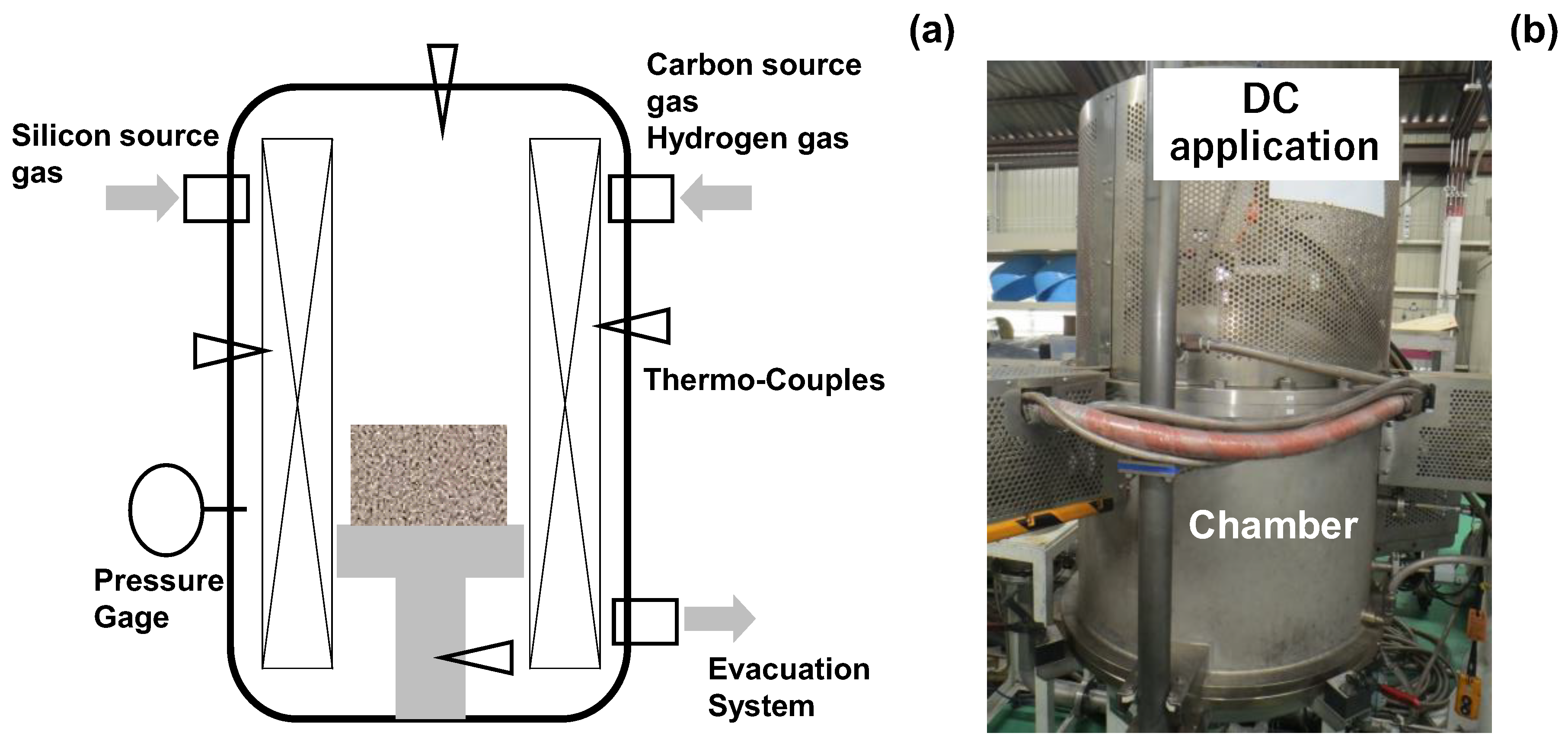
A thermal CVD system (Shinko-Seiki, Co., Ltd., Kobe, Japan) was used to achieve the carbon supersaturation of the co-deposited SiC coating onto the sintered SiC die substrate by controlling the carbon source gas flow rate. As illustrated in Figure 2a, a sintered SiC block with an average porosity of 0.5% was prepared as a substrate to make a thick SiC coating via the thermal CVD process at 1500 K for 108 ks. Silicon chloride and methane gases were selected as the silicon and carbon sources, respectively. They were mixed with hydrogen gas and introduced at a total flow rate of 500 mL/min to the thermal reactor in the CVD system. The average deposition rate was 37 μm/ks; the thickness of the SiC coating reached 4 mm.
After cooling down in an inert gas atmosphere, the SiC-coated SiC block was directly cut using a diamond saw and polished using chemical buffing to shape the SiC-coated SiC punch and die. An overview of thermal CVD system is depicted in Figure 2b.

2.2. Preparation of Specimens for Microstructure Analyses

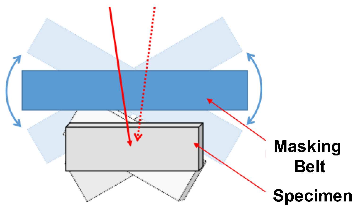
The MCSed SiC coating die was ion-sliced and ion-milled to prepare a specimen for STEM analysis [14]. To avoid anisotropic milling, the masking belt was rotated during the ion-slicing step to build up the specimen, as shown in Figure 3. After the ion milling, the specimen surface was adjusted and polished for STEM analysis.

2.3. CNC-Upsetting of Work Materials

The CNC stamping system (MT-1; Precise Stamping Laboratory, LLC, Tokyo, Japan) was utilized for cold forging.
As illustrated in Figure 4a, a titanium feedstock bar was upset using the MCSed SiC punch and die in the following forging experiments. The reduction in thickness was controlled by the stroke between the upper and lower bolsters. The MCSed punch and die were cemented to each bolster, respectively, as shown in Figure 4b,c. The cross-sectional view of the MCSed die is also depicted in Figure 4d; a 6H-structured SiC layer was coated onto the sintered SiC substrate with a thickness of 4 mm.
In the case of warm forging, an IH (induction heating) unit (YS-Electrical Industry, Co., Ltd., Kofu, Japan) was used for rapid heating and maintaining the temperature.

3. Results

The detail mechanisms from Stage I to Stage III are explained using STEM analysis and the continuous forging experiments in dry and cold. The friction coefficient of the contact interface between the MCSed die and titanium work is also estimated.

3.1. Characterization of the MCS Process

XRD was utilized to characterize the massive carbon supersaturation (MCS) into SiC coating. MCSed and normal SiC coatings were analyzed by XRD (Rigaku SmartLab, Rigaku, Co., Ltd., Tokyo, Japan) with monochromatic CuKa radiation (λ = 0.1542 nm) and Bragg–Brentano geometry, at 40 kV and 30 mA. The 2θ range was set between 20 and 80°, with a scanning speed of 10 mm/min and a step angle of 0.02°. As stated by the micromechanics in [15], the lattice strain is sensitive to inhomogeneities embedded into the grains.
Figure 5 depicts the measured XRD diagram of SiC coating on the sintered SiC substrate between the bare SiC and MCSed SiC coating dies. The normally CVD-coated SiC is characterized by three peaks; e.g., SiC (111) at 2θ = 35.938°, SiC (200) at 2θ = 60.237°, and SiC (331) at 2θ = 71.985°, with reference to [16]. This XRD reveals that the CVD-synthesized coating is β-phase SiC and has a cubic structure. Through the MCS with co-deposition of βSiC onto the SiC block, these peaks shifted; e.g., βSiC (111) shifted to 2θ = 35.56°, and βSiC (220) shifted to 2θ = 60.034°. This MCS is characterized by the lattice expansion of SiC. Inhomogeneity is present inside βSiC grains, inducing a positive lattice strain. Later, a precise microstructural analysis is employed to describe this inhomogeneity in SiC that induces this lattice expansion.

3.2. Granular Structure with and without MCS

In addition to the inhomogeneities inside SiC grain, other inhomogeneities are possible to locate at the SiC grain boundaries. When these are distributed along the boundaries of SiC grains and at their triplet corners during CVD, each grain growth is significantly suppressed by their pinning effect [17]. Hence, the SiC grain size distribution provides a means to detect the presence of inhomogeneities along the SiC grain boundaries.
Figure 6 compares the laser microscopic images on the CVD SiC coating with and without MCS. Without MCS treatment, lots of irregular-shaped and extraordinarily grown SiC grains can be seen in Figure 6a. On the other hand, most SiC grains adjusted to a homogeneous distribution of fine grains, as shown in Figure 6b. This implies that extraordinary SiC grain growth was suppressed by this MCS treatment of SiC grains during the CVD process.

3.3. Formation of Carbon-Rich Clusters in MCSed SiC Die

STEM analyses with SEM-EDS were performed to identify what the representatives of these inhomogeneities are inside SiC grains and along the grain boundaries. Figure 7 shows a typical microstructure of an MCSed SiC coating. Two defects were found in this TEM image; i.e., the stacking faults penetrating across the SiC grain from one end of grain boundary (GB) to the other GB, and the clusters located at the vicinity of the SiC grain boundaries (GBs). The selected area electron dispersive (SAED) X-ray image, inserted in Figure 7, shows that the CVD-synthesized SiC grains had a 6H structure among the candidate crystallographic morphologies [18]. These defects were synthesized by MCS into this 6H-structured SiC granular structure.
These clusters, identified by the red arrow in Figure 7, were further analyzed by STEM and EDX. Figure 8a depicts a STEM image of the SiC coating, including three clusters with a size of 1 μm, most of which were located along the SiC grain boundaries. According to EDS analysis, these three clusters mainly consisted of carbon, as shown in Figure 8b,c. During the CVD process, the excess carbons were supersaturated into the SiC nucleates. Each SiC nucleate was lattice-strained by this carbon supersaturation to eject these carbon solutes from the inside of SiC nucleate to its boundaries. This self-ejection process left defects inside the SiC grains after the CVD process.
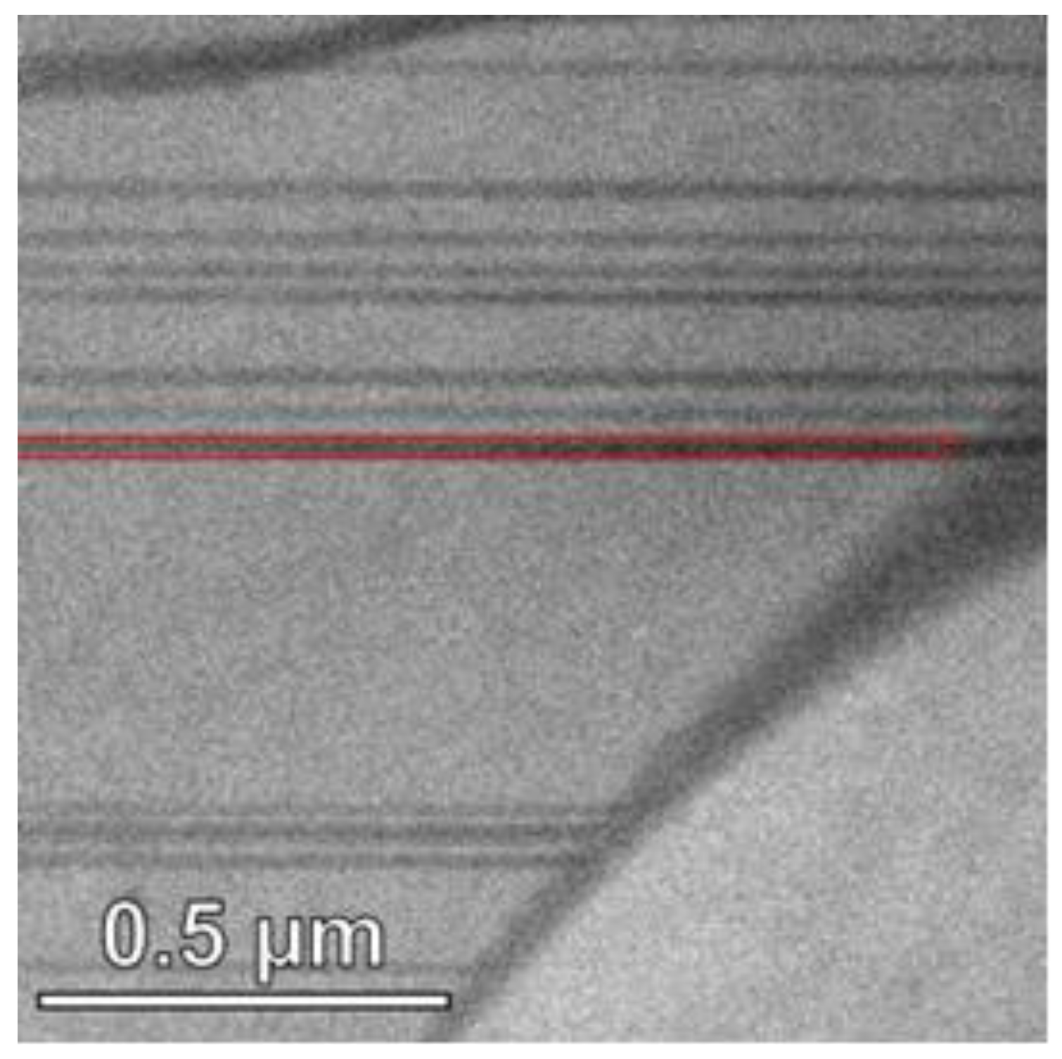
Figure 9 depicts an array of stacking faults penetrating through the 6H-structured SiC grain from one end of the GB to the other end of the GB. Most of the supersaturated carbons were ejected into the GBs by this formation of stacking faults, forming carbon-rich clusters along the GBs. Through this ejection, the lattice strains induced by MCS inside the SiC grains are relaxed by the formation of stacking faults.

3.4. Transportation of Free Carbons to Contact Interface

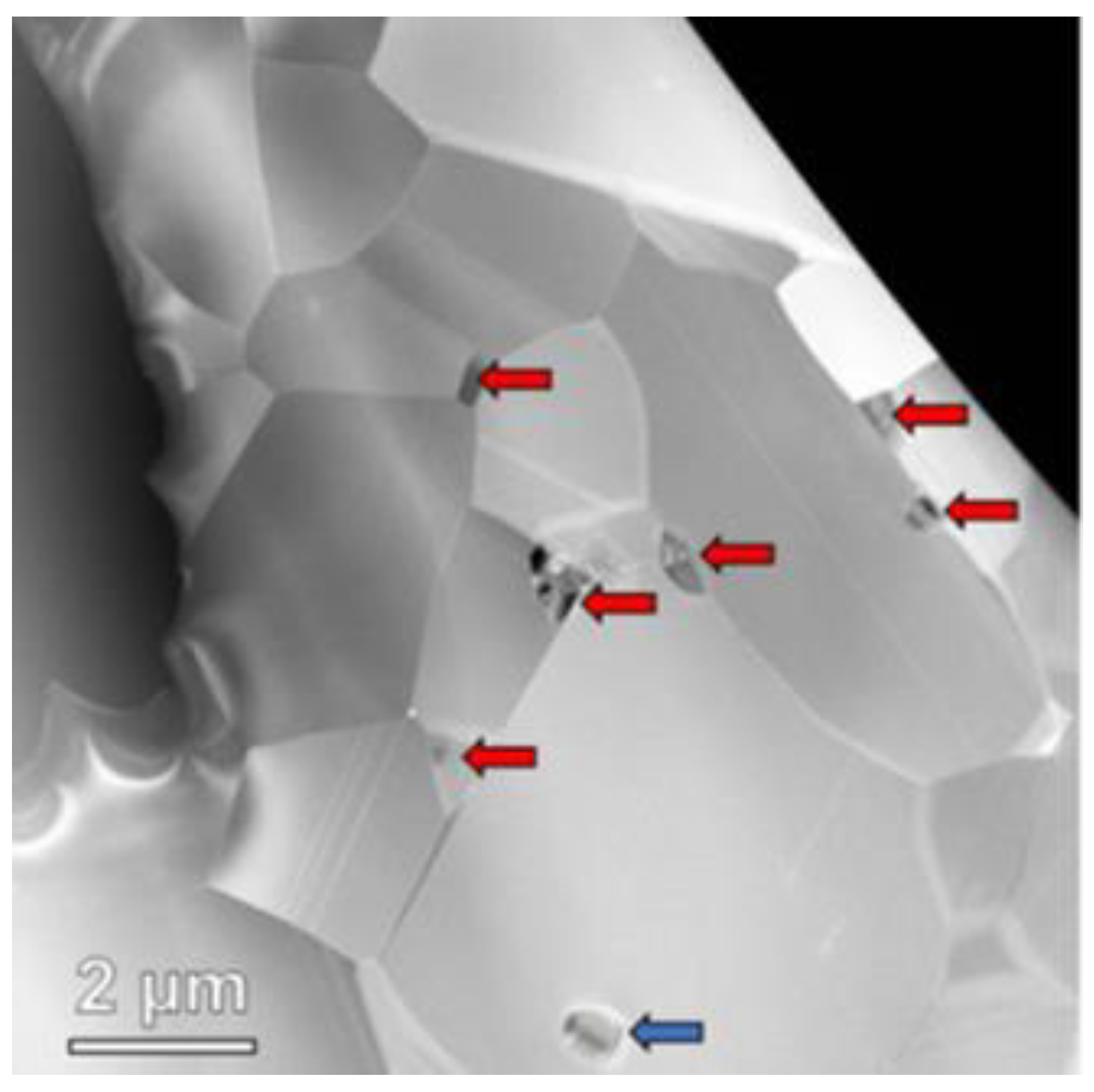
The MCSed SiC coating is identified as a composite, where 6H-strcutured SiC grains, including their stacking fault array inside, have lots of carbon-rich clusters along their GBs. This composite granular structure is shown in Figure 10.
Each SiC grain has lots of carbon-rich clusters along every GB. In addition, a few carbon-rich clusters are included inside SiC grains, expanding the lattice structure, as depicted as a peak shift in Figure 5. Each cluster along the GBs neighbors another one within 1 to 2 μm, as shown in Figure 10. When high traction is applied to the surface of this composite SiC coating die, some clusters are elastically strained, expelling the carbon solutes along the neighboring GBs due to the stress gradient across the coating thickness. As stated in [19], these carbons isolated from clusters are transported to highly stressed hot spots on the contact interface. These GBs work as diffusion paths for carbon solutes.

3.5. Formation of Carbon Agglomerates at Hot Spots on the Contact Interface

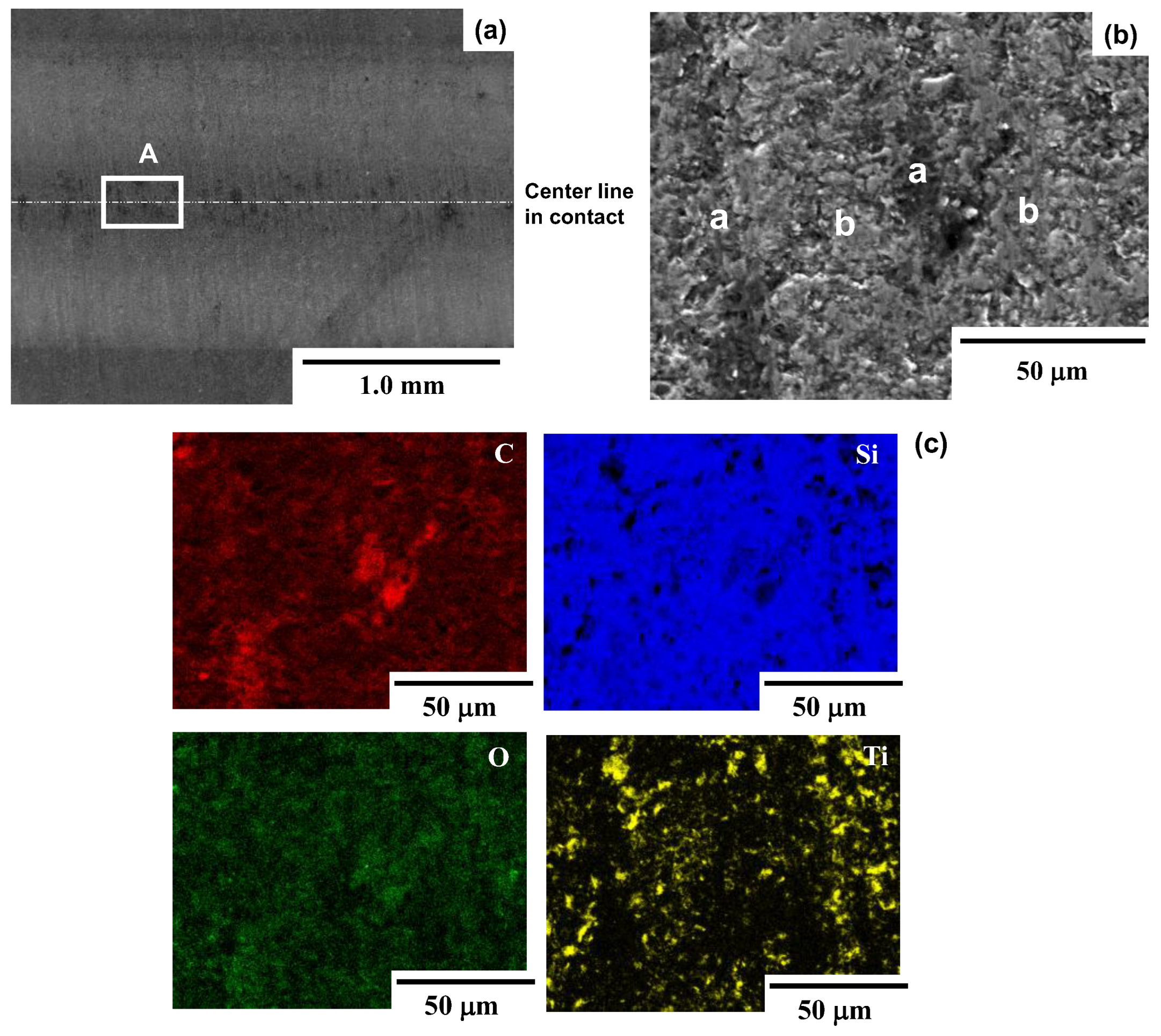
A dry, cold upsetting experiment was performed to investigate the frictional behavior on the contact interface between the MCSed SiC coating die and pure titanium wires. A pure titanium wire with a diameter of 1.0 mm and length of 10.0 mm was upset within a single stroke up to specified reductions in thickness (r) of r = 10%, 20%, 30%, 50%, and 70%, respectively. In addition, a continuous upsetting experiment was also performed 20 times until r = 70% to describe the adhesive behavior of titanium fresh debris on the contact interface of the MCSed SiC die. SEM-EDS was also used to analyze this adhesion process during continuous upsetting experiments. Figure 11 depicts the SEM image and element mapping at the hot spots on the contact interface after continuous upsetting.
As shown in Figure 11a, the white and gray lines are aligned in the direction of the metal flow on the contact interface. In particular, these lines are classified as the a- and b-phases at the A region of the interface, as shown in Figure 11b; e.g., the a-phase corresponds to white and gray lines in Figure 11a, and the b-phase is identified as interfaces other than a-phase. The element mapping in Figure 11c reveals that the a-phase consisted of carbon films on the SiC. Since Si was weakly detected at the a-phase zones, these carbon films formed thickly on the SiC die. In addition, the whole carbon film was formed as an assembly of carbon agglomerates with an average size of 5 μm. Remembering that the average SiC grain size ranges from 2 to 5 μm, these agglomerates must have been made from the carbon solutes ejected from the GBs of the SiC grains shown in Figure 10. Since oxygen and titanium map coincide with each other, the b-phase was composed of the titanium oxide. That is, the thick carbon films and the thin titanium oxide layers were formed on the contact interface between the MCSed SiC die and the continuously upset titanium wires.
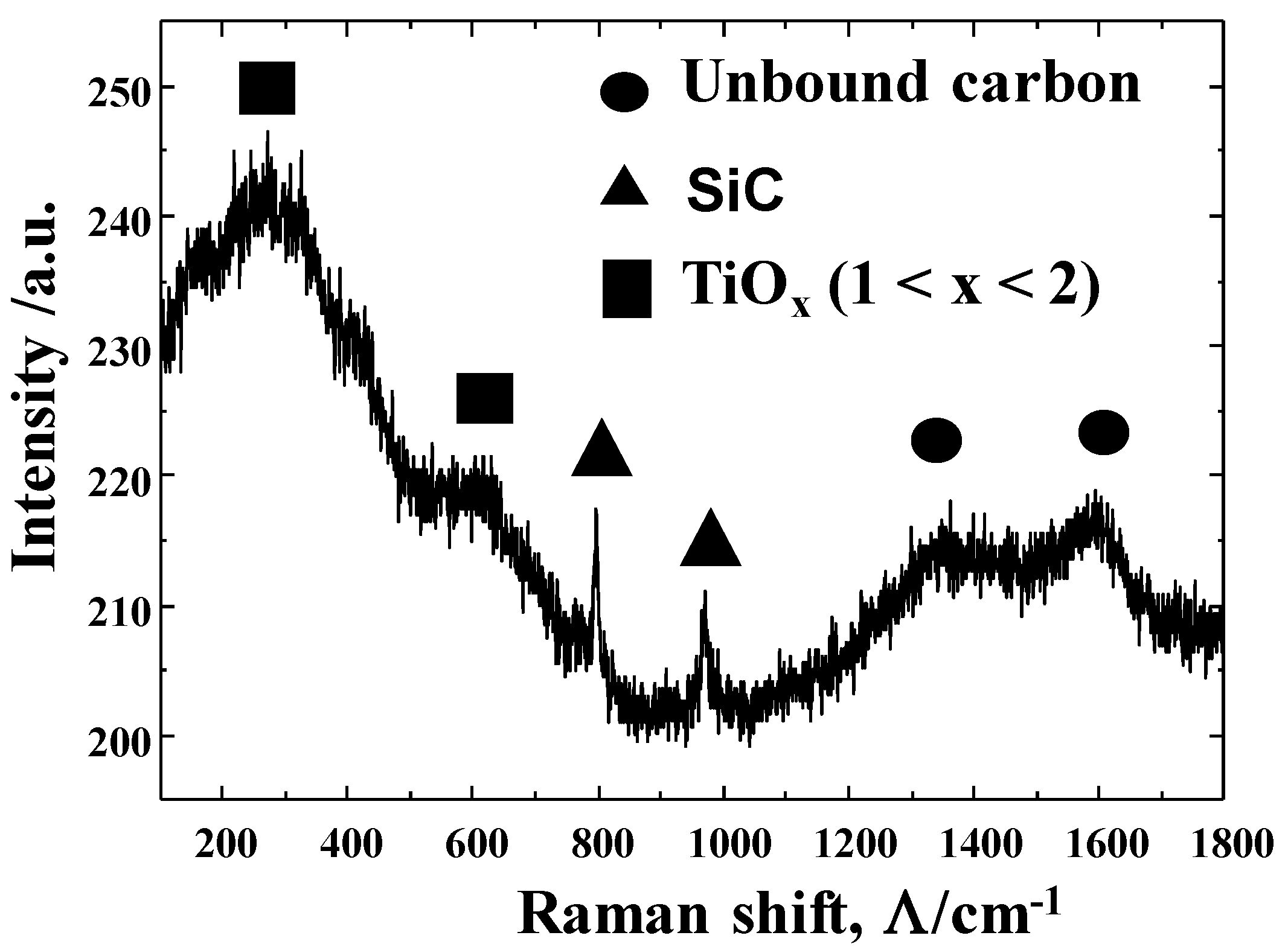
Raman spectroscopy was utilized to characterize the local material distribution at the center of the contact interface shown in Figure 11. Figure 12 shows that two materials were distributed on the SiC coating. Two narrow peaks at Λ = 800 cm−1 and 950 cm−1, respectively, with weak intensities, reveal that the βSiC die surface was partially covered by these two materials. Free carbon was detected as two broad peaks, the D-peak at Λ = 1330 cm−1 and the G-peak at Λ = 1600 cm−1 [20]. Other than these two peaks, only a broad peak was detected around Λ = 200~600 cm−1. The titanium and oxygen maps were detected by EDS except for the carbon map on the contact interface shown in Figure 11c. These broad peaks might correspond to titanium oxide. If TiO2 was only present as titanium oxide at the interface, narrow peaks could be detected at Λ = 400 cm−1 and 600 cm−1, respectively, after [21]. These narrow peaks cannot be observed in Figure 12, implying that titanium oxide film consists of various binding states in the titanium–oxygen system from TiO to TiOx for 1 < x < 2, through the intermediate Magneli phase oxides [22]. In particular, the other broad peaks at Λ = 150 cm−1 and 250 cm−1 suggest that the intermediate titanium oxides or TiOx are formed together with TiO2 debris particles in the tribofilm.
XPS (X-ray photoelectron spectroscopy) was utilized to investigate the binding energy of Ti–O in these oxides. Three Ti 3/2 peaks were detected for TiO, TiOx, and TiO2. In these binding energies, 455 eV represents TiO, 457 eV corresponds to TiOx, and 459 eV represents TiO2.
The SEM-EDS and Raman spectroscopic analyses in the above section revealed that thick free-carbon layers and agglomerates work as a tribofilm at the hot spots on the contact interface together with the thin lines of deformable titanium oxide, TiOx. This in situ formation of free-carbon tribofilm influences the titanium metal flow on the contact interface.

3.6. Frictional Behavior in Upsetting of Pure Titanium Wires Using MCSed SiC Dies

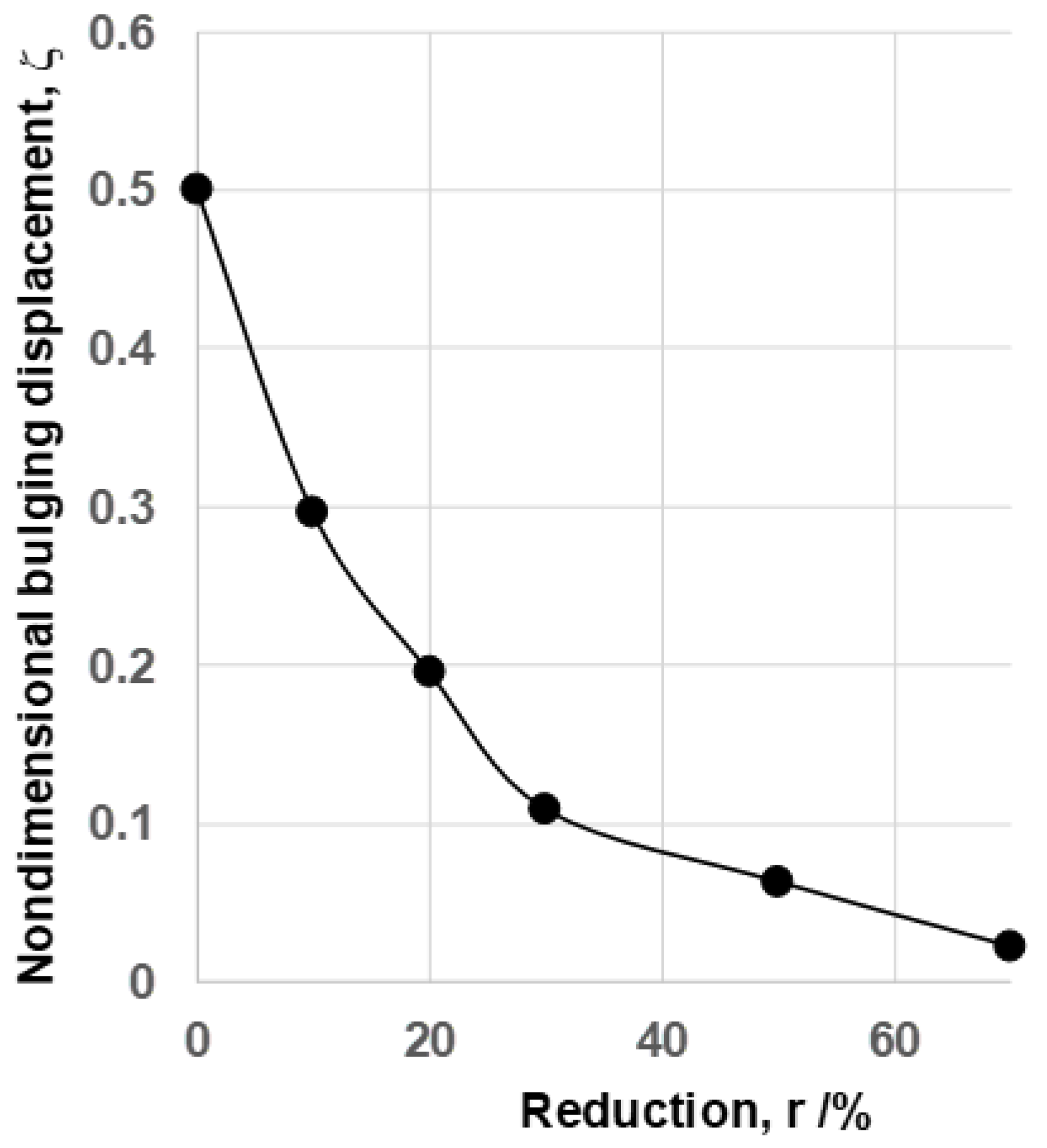
The upsetting of pure titanium wires to specified reductions in thickness was performed to describe the effect of in situ-formed free-carbon tribofilm on the frictional behavior. By increasing the reduction in thickness (r), the wire width (Wo) and the contact interface width (Wi) increased during the upsetting. When the friction coefficient (μ) was higher than unity, or μ >> 1.0, the non-dimensional bulging displacement (ζ), which is defined by ζ = (Wo − Wi)/2Wο, was nearly the same as ζ~0.5, irrespective of r. On the other hand, when μ << 1.0, ζ rapidly decreased to 0.0 with r. Hence, the relationship of ζ to r provides a means to estimate the frictional state on the contact interface.
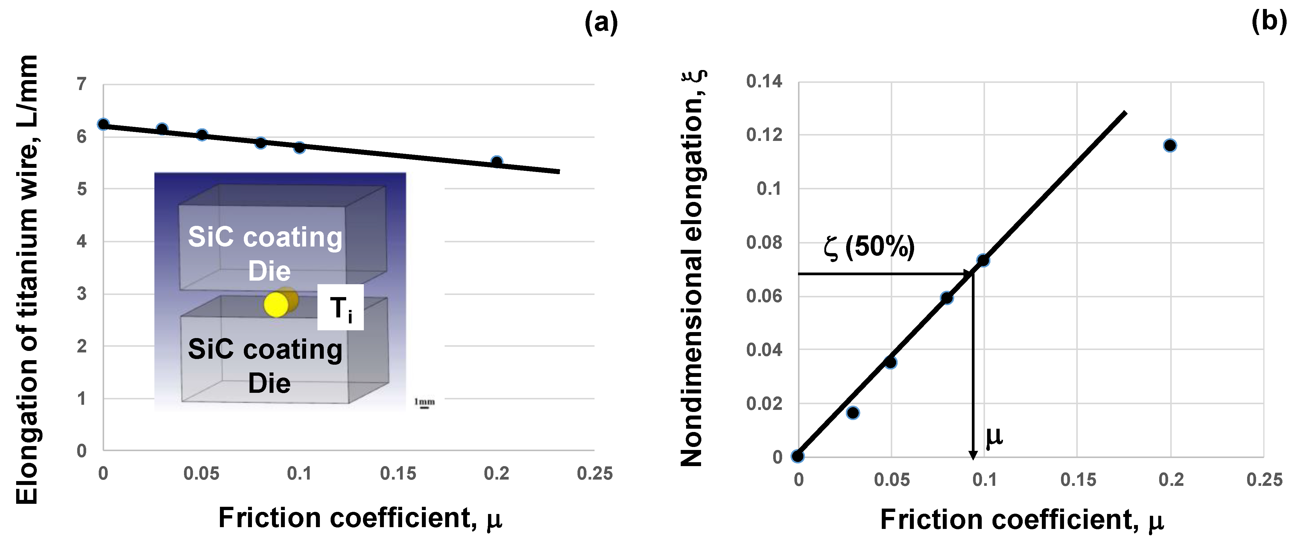
The Wo and Wi of the upset titanium wires at each r were measured in the upsetting experiment to deduce the relationship between ζ and r. As shown in Figure 13, ζ decreased exponentially with r up to r = 30%, and gradually deceased with r for r > 30%. This implies that the friction coefficient steeply reduced with r due to the homogeneous metal flow on the contact interface for r < 30%, and that the workpiece flattened with r in the low frictional state for r > 30%. Referring to [23], the friction coefficient was empirically estimated from this ζ (r) relationship in Figure 13 to be μ = 0.05 to 0.1. For quantitative analysis of the friction coefficient for r > 30%, inverse finite element analysis was performed according to [24,25]. Three-dimensional finite element analysis was employed to parametrically vary the friction coefficient for 0 < μ < 0.2 and to estimate μ at r = 50% to calculate the nondimensional elongation, ξ (μ, 50%), coinciding with the experimentally measured nondimensional bulging displacement, ζ (50%).
Figure 14a depicts the linear variation in the elongation L (μ, 50%) for the titanium workpiece with the friction coefficient. These elongations were calculated assuming the die material was rigid and the titanium workpiece behaved in rigid–plastic manner. These L’s for each μ were edited to the nondimensional elongation, ξ (μ, 50%), as shown in Figure 14b. Since ζ (50%) = 0.07, according to Figure 13, μ was estimated to be 0.09, according to Figure 14b.
We validated this estimated friction coefficient by comparing the calculated equivalent plastic strain distribution in the cross-section of the upset titanium workpiece at r = 50% with the use of μ = 0.09 and the measured hardness map in the cross-section of the upset titanium wire at r = 50%. Both are in good agreement, as shown in Figure 15. This proves that the estimated friction coefficient, μ = 0.09, is adaptive to the metal flow and work-hardening behavior during the upsetting process.

4. Discussion

In reference to a general scheme on the in situ solid lubrication model in Figure 1, let us describe a detailed mechanism of in situ solid lubrication in dry, cold forging of pure titanium using the MCSed SiC coating dies. In Stage I, carbon-rich clusters form inside the SiC grains and along the SiC grain boundaries during the CVD process. The former clusters induce the SiC grain lattice expansion, which was detected by the peak shifts in the XRD diagrams. The latter clusters work as a pinning site to suppress the extraordinary SiC grain growth. Since the excess carbon solutes agglomerate inside the SiC grains to each grain boundary, this diffusion path is left as a stacking fault, which penetrates from one end of the grain boundary to the other. Then, except for the carbon solutes housed inside the SiC grains, most of the carbon solutes are preserved along the SiC grain boundaries.
In Stage II, each SiC grain, with every grain boundary enriched by carbon-rich clusters, are stressed from the contact interface with the work materials. As suggested in [26], these clusters are compressed and sheared to squeeze the carbon solutes through the grain boundaries to the contact surface. As seen in Figure 11, these solutes form the carbon agglomerates at the hot spots on the contact surface.
In Stage III, the in situ-formed carbon agglomerates work as a solid lubricant to preserve the low frictional state on the contact interface. These agglomerates are aligned in the direction of the metal flow, suppressing the adhesion of the titanium fresh surface to the SiC coating die during the upsetting.
As predicted by [27], this in situ solid lubrication process is expected to work in hot forging and stamping. The amount of carbon solutes in this in situ formation of tribofilm is negligibly small enough to achieve zero emissions in hot forging and stamping operations. In particular, refractory metals and alloys, as well as high-transition-temperature oxide glasses, are near-net forged and mold-stamped without any increase in environmental burdens.
After systematic BOD testing using the pure titanium balls in dry conditions, the Coulomb friction coefficients of various coatings were reported in [28]. For TiN, TiAlN, and TiCN coatings, μ >> 1.0 due to severe galling on the contact surfaces. This high friction came from the adhesion of the titanium ball to the titanium-transferred coating surface. In the case of a Si-bearing DLC (diamond-like carbon) coating, 0.5 < μ < 0.7 with metallic sticking. The nano-laminated DLC had μ~0.2, in a similar manner to other structured DLCs [29]. It is difficult for these DLC coatings to be completely free from galling at hot spots on the sliding tracks. Using the MCSed SiC coating die, μ~0.09, much lower than those coating surfaces. This implies that the local adhesion of titanium fresh debris at the hot spots is suppressed by the in situ formation of free-carbon tribofilms. Hence, the flow stress of titanium has nothing to do with the measured Coulomb friction coefficient; therefore, there is no need to use the shear friction coefficient.
As stated in [30], the friction coefficient can be reduced from 0.01 to 0.001 by using a superlubricating coating; however, most of them cannot be free from galling in the process tribology.
Since 6H-structured SiC has high thermal resistance, high hardness, and thermal conductivity, this MCSed SiC coating die is utilized as a die for the hot mold-stamping of visco-elastic oxide glass melts into optical elements [8] and for the hot forging of refractory metals and alloys [31]. As experienced in hot mold-stamping with the use of WC (Co) and AISI316 dies, the adhesive wear or galling of the glass melts onto those dies resulted in fatal failure of the dies [32]. However, by using these MCSed SiC coating dies, the in situ free-carbon tribofilm formed at the hot spots prevents the die surface from having direct contact with visco-plastically deforming glass melts and preserves the well-designed die surface structure for DOEs. In addition, the free-carbon tribofilms are only formed at the hot spots under high surface traction; the amount of carbon residuals on the mold-stamped optical elements can be minimized enough to be easily polished away from products.
By increasing the carbon source gas flow rate during CVD, more carbon-rich clusters are expected to be distributed along the fine SiC grain boundaries. At the limit where the whole grain boundaries are overlapped by these carbon-rich clusters, these grain boundaries become fragile enough to make self-delamination from the SiC base coating layer and to yield the 6H-structured SiC coating substrates. This selective carbon source content control in CVD provides a new way to yield the polycrystalline 6H-structured SiC substrates with refined granular structure and high density.

5. Conclusions

A 6H-structured SiC coating with a thickness of 4 mm was synthesized by CVD with carbon content control and yielded as a die for the cold, dry forging of pure titanium feedstocks. Massive carbon supersaturation in CVD induces carbon-rich clusters inside of the 6H-structured SiC grains and along their grain boundaries and triplet corners. These clusters work as an inhomogeneity to expand the SiC lattices, characterized by a peak shift in XRD. The latter clusters act as a pinning site to suppress the SiC grain growth during CVD and to homogenize the SiC grains. These clusters form as inhomogeneities inside SiC nucleates during CVD; most of them are exiled from inside SiC nucleates to their boundaries, in parallel with the formation of lots of stacking faults inside.
The MCSed SiC coating die consists of 6H-structured fine SiC grains and carbon-rich clusters inside the SiC grain boundaries. This composite microstructure has the potential to supply a free-carbon solute yield in Stage I during the in situ solid lubrication mechanism. During the forging process, the free-carbon solutes isolate from carbon-rich clusters along the grain boundaries and transport themselves to the contact interface by the stress gradient in Stage II. The free-carbon tribofilm is co-formed in situ with deformable titanium oxides to preserve the low frictional state on the contact interface and to prevent the SiC die from severe galling to titanium fresh debris in Stage III. Due to the high heat resistance and thermal conductivity of 6H-structured SiC grains, this MCSed SiC coating is useful for the hot forging of refractory metals and alloys and oxide glasses with high glass-transition temperature.

Author Contributions

Conceptualization, T.A.; methodology, T.A.; validation, T.A. and T.F.; formal analysis, T.A. and T.F.; investigation, T.A. and T.F.; resources, T.F.; writing—original draft preparation, T.A.; writing—review and editing, T.A. and T.F.; supervision, T.F.; project administration, T.F. All authors have read and agreed to the published version of the manuscript.

Funding

This research received no external funding.

Data Availability Statement

The original contributions presented in the study are included in the article, further inquiries can be directed to the corresponding author.

Acknowledgments

The authors would like to express their gratitude to T. Koyama, M. Saito, H. Yoshida, and Y. Ikuhara (University of Tokyo) for their sincere efforts in STEM analysis.

Conflicts of Interest

Author Tatsuya Fukuda was employed by Tokai Engineering Service, Co., Ltd. The remaining author declares that the research was conducted in the absence of any commercial or financial relationships that could be construed as a potential conflict of interest.

References

  1. Xu, M.; Girish, Y.R.; Rakesh, K.P.; Wu, P.; Manukumar, H.M.; Byrappa, S.M.; Udayabhanu Byrappa, K. Recent advances and challenges in silicon carbide (SiC) ceramic nanoarchitectures and their applications. Mater. Today 2021, 28, 102533. [Google Scholar] [CrossRef]
  2. Schöne, J.; Beckert, W.; Matthey, B.; Herrmann, M. Modelling of the microstructure and thermal conductivity of SiC-bonded diamond materials. Open Ceram. 2024, 18, 100594. [Google Scholar] [CrossRef]
  3. Nakamura, D.; Gunjishima, I.; Yamaguchi, S.; Ito, T.; Okamoto, A.; Kondo, H.; Onda, S.; Takatori, K. Ultrahigh-quality silicon carbide single crystals. Nature 2004, 430, 1009–1012. [Google Scholar] [CrossRef] [PubMed]
  4. Raju, K.; Yoon, D.-H. Sintering additives for SiC based on the reactivity: A review. Ceram. Int. 2016, 42, 17947–17962. [Google Scholar] [CrossRef]
  5. Kaloyeros, A.E.; Arkles, B. Review—Silicon Carbide Thin Film Technologies: Recent Advances in Processing, Properties, and Applications: Part II. PVD and Alternative (Non-PVD and Non-CVD) Deposition Techniques. 2024 ECS J. Solid State Sci. Technol. 2024, 13, 043001. [Google Scholar] [CrossRef]
  6. Wang, Y.; Sun, J.; Sheng, B.; Cheng, H. Deposition mechanism and Thickness Control of CVD SiC Coatings on NextelTM440 Fibers. Coating 2024, 10, 480. [Google Scholar] [CrossRef]
  7. Cheng, Z.; Liang, J.; Kawamura, K.; Zhou, H.; Asamura, H.; Uratani, H.; Tiwari, J.; Graham, S.; Ohno, Y.; Nagai, Y.; et al. High thermal conductivity in wafer-scale cubic silicon carbide crystals. Nat. Commun. 2020, 13, 7201. [Google Scholar] [CrossRef]
  8. Zhou, T.; He, Y.; Wang, T.; Zhu, Z.; Xu, R.; Yu, Q.; Zhao, B.; Zhao, W.; Liu, P.; Wang, X. A review of the techniques for the mold manufacturing of micro/nanostructures for precision glass molding. Int. J. Extrem. Manuf. 2021, 3, 042002. [Google Scholar] [CrossRef]
  9. Li, Y.; Nie, Y.; Xue, S.; Hu, C.; Xiang, C.; Su, X.; Luo, J.; Li, S.; Yu, Z. Abnormal grain growth in iron-containing SiC fibers. J. Euro. Ceram. Soc. 2021, 41, 2306–2311. [Google Scholar] [CrossRef]
  10. Wang, X.; Li, H.; Liu, H.; Cao, K.; Xia, S.; Zhong, Y.; Yang, T. Growth and defect formation mechanism of CVD-prepared SiC coatings based on cross-scale simulation. Chem. Eng. J. 2024, 479, 147652. [Google Scholar] [CrossRef]
  11. Aizawa, T.; Koh-Ichi Itoh, K.-I.; Fukuda, T. SiC-coated SiC die for galling-free forging of pure titanium. Mater. Trans. 2020, 61, 282–288. [Google Scholar] [CrossRef]
  12. Aizawa, T.; Ito, K.-I.; Fukuda, T. Galling-free micro-forging of titanium wire with high reduction in thickness by β-SiC dies. In Forming the Future; The Minerals, Metals & Materials Series; Springer: Cham, Switzerland, 2021; pp. 1065–1075. [Google Scholar]
  13. Aizawa, T.; Yoshino, T.; Fukuda, T.; Shiratori, T. Dry cold forging of pure titanium wire to thin plate with used of β-SiC coating dies. J. Mater. 2020, 13, 3780. [Google Scholar] [CrossRef] [PubMed]
  14. JEOL. New Preparation of Samples for STEM Analysis with Low Strains and Damages by Ion-Slicing Technique with the Use of Masking Belt. Available online: https://www.jeol.co.jp/solutions/applications/details/1103.html (accessed on 2 July 2024).
  15. Mura, T.; Mori, T. Introduction to Micromechanics; Baifu-Kan Press: Tokyo, Japan, 1985. [Google Scholar]
  16. Ortiz, A.L.; Sánchez-Bajo, F.; Cumbrera, F.L.; Guiberteau, F. X-ray powder diffraction analysis of a silicon carbide-based ceramic. Mater. Lett. 2001, 49, 137–145. [Google Scholar] [CrossRef]
  17. Moelans, N.; Blanpain, B.; Wollants, P. Pinning effect of second-phase particles on grain growth in polycrystalline films studied by 3-D phase field simulations. Acta Mater. 2007, 55, 2173–2182. [Google Scholar] [CrossRef]
  18. Arzig, M.; Salamon, M.; Uhlmann, N.; Wellmann, P.J. Investigation of the growth kinetics of SiC crystals during physical vapor transport growth by the application of in situ 3D computed tomography visualization. Advan. Eng. Mater. 2020, 22, 1900778. [Google Scholar] [CrossRef]
  19. Peng, Y.; Gong, J.; Jiang, Y.; Rong, D.; Fu, M. Numerical analysis of stress-induced concentration-dependent carbon diffusion in low-temperature surface carburisation of 316L stainless steel. Int. J. Comp. Mater. Sci. Surf. Eng. 2019, 8, 101663. [Google Scholar] [CrossRef]
  20. Wang, Y.; Alsmeyer, D.C.; McCreery, R.L. Raman spectroscopy of carbon materials: Structural basis of observed spectra. Chem. Mater. 1999, 2, 557–563. [Google Scholar] [CrossRef]
  21. Data Were Retrieved. Available online: https://www.researchgate.net/figure/Micro-Raman-spectra-of-TiO-2-and-TiO-2-SiC-composites_fig3_260938953 (accessed on 3 June 2024).
  22. Wills, R.G.A.; Walsh, F.C. A review of the continued development of Magneli phase titanium oxides and Ebonex® for electrochemical applications. Electrochim. Acta 2010, 55, 6342–6351. [Google Scholar]
  23. Hong, J.-J.; Yeh, W.-C. Application of response surface methodology to establish friction model of upset forging. Adv. Mech. Eng. 2018, 10, 1687814018766744. [Google Scholar] [CrossRef]
  24. Franchi, R.; Prete, A.D.; Umbrello, D. Inverse analysis procedure to determine flow stress friction data for finite element modeling of machining. Int. J. Mater. Forming 2017, 10, 685–695. [Google Scholar] [CrossRef]
  25. Ishiguro, S.; Aizawa, T.; Funazuka, T.; Shiratori, T. Green forging of titanium titanium alloys by using the carbon supersaturated SKD11 dies. J. Appl. Mech. 2022, 3, 724–739. [Google Scholar] [CrossRef]
  26. Moskalioviene, T.; Galdikas, A. Stress induced and concentration dependent diffusion of nitrogen in nitrided austenitic stainless steel. Comp. Mater. Sci. 2012, 86, 1552–1557. [Google Scholar] [CrossRef]
  27. Dohda, K.; Boher, C.; Rezai-Aria, F.; Mahayotsanun, N. Tribology in metal forming at elevated temperatures. Friction 2015, 3, 1–27. [Google Scholar] [CrossRef]
  28. Dohda, K.; Aizawa, T. Tribo-characterization of silicon doped and nano-structured DLC coatings by metal forming simulators. Manuf. Lett. 2014, 2, 82–85. [Google Scholar] [CrossRef]
  29. Nunthavarawong, P.; Rangappa, S.M.; Siengchin, S.; Dohda, K. Diamond-Like Carbon Coatings -Technologies and Applications; CRC-Press: Boca Raton, FL, USA, 2023. [Google Scholar]
  30. Tasdemir, H.A.; Wakayama, M.; Tokoroyama, T.; Kousaka, H.; Umehara, N.; Mabuchi, Y.; Higuchi, T. Ultra-low friction of tetrahedral amorphous diamond-like carbon (ta-C DLC) under boundary lubrication in poly alpha-olefin (PAO) with additives. Tribol. Int. 2013, 65, 286–294. [Google Scholar] [CrossRef]
  31. Beal, J.D.; Boyer, R.; Sandes, D. Forming of titanium and titanium alloys. In ASM Handbook 14B: Metal Working/Sheet Forming; ASM International: Materials Park, OH, USA, 2006; pp. 656–669. [Google Scholar]
  32. Zhao, H.; Gain, A.K.; Li, Z.; Zhang, L. Wear of mold surfaces: Interfacial adhesion in precision glass molding. Wear 2023, 524–525, 204847. [Google Scholar] [CrossRef]
Figure 1. The in situ solid lubrication mechanism during the upsetting of titanium bars with the use of an MCSed SiC coating die. (a) Stage I: The isolation of carbon from the MCSed SiC grains. (b) Stage II: The diffusion of isolated carbon solutes to the hot spots on the contact interface. (c) Stage III: The formation of carbon agglomerates on the contact interface of the MCSed SiC die on the titanium bars.
Lubricants 12 00309 g001
Figure 2. A thermal CVD processing system. (a) Its schematic view, and (b) its overview.
Lubricants 12 00309 g002
Figure 3. Ion milling with the use of a masking belt to avoid anisotropic etching of the MCSed SiC coating die.
Lubricants 12 00309 g003
Figure 4. CNC stamping system for upsetting the titanium wires. (a) Schematic view of the experimental setup, (b,c) overview of the real setup of upper and lower SiC dies, and (d) cross-sectional view of SiC coating die with a coating layer thickness of 4 mm.
Lubricants 12 00309 g004
Figure 5. Comparison of XRD diagrams for βSiC with and without MCS. (a) XRD diagram of normal βSiC, and (b) XRD diagram of MCSed βSiC (Red lines represent the measured profile, and blue lines indicate the peak positions).
Lubricants 12 00309 g005
Figure 6. Comparison of LM images for single-phase SiC coatings with and without the massive carbon supersaturation. (a) LM image of CVD SiC coating without MCS, and (b) LM image of MCSed SiC with MCS.
Lubricants 12 00309 g006
Figure 7. Modified microstructure of polycrystalline SiC by massive carbon supersaturation. The blue arrow indicates a stacking fault induced within the SiC grains. The red arrow points at a cluster in the vicinity of the grain boundary. The SAED pattern at P1 in Figure 7 is also inserted in the lower right corner.
Lubricants 12 00309 g007
Figure 8. Carbon enrichment to form the carbon-rich clusters along the MCSed SiC GBs. (a) STEM image, (b) silicon mapping, and (c) carbon mapping.
Lubricants 12 00309 g008
Figure 9. Formation of the stacking faults penetrating from one MCSed-SiC GB to another.
Lubricants 12 00309 g009
Figure 10. Dense distribution of carbon-rich clusters along the SiC GBs and inside SiC grains. The red arrows indicate the carbon-rich clusters along the GBs, and the blue arrow points to a carbon-rich cluster inside a SiC grain.
Lubricants 12 00309 g010
Figure 11. SEM-EDS analysis on the contact interface of the MCSed SiC die to the upset titanium works after continuously upsetting the titanium wires 20 times until r = 70%. (a) SEM image of the contact interface with low magnification; (b) SEM image of the hot spots in the A region in (a), and (c) element mapping by EDS.
Lubricants 12 00309 g011
Figure 12. Raman spectra measured at the A region in Figure 11a. Unbound carbon, titanium oxide of TiOx for 1 < x < 2, and SiC were detected.
Lubricants 12 00309 g012
Figure 13. Variation in the measured nondimensional bulging displacement, ζ, with the reductions in thickness (r) during the upsetting experiment with the use of MCSed SiC coating dies.
Lubricants 12 00309 g013
Figure 14. Inverse analysis to estimate the friction coefficient, μ, on the contact interface between the MCSed SiC die and the upset titanium workpiece. (a) Calculation of the elongation of the titanium workpiece by varying the friction coefficient parametrically for 0 < μ < 0.2, and (b) direct estimate of μ for ξ (μ, 50%) = ζ (50%).
Lubricants 12 00309 g014
Figure 15. Comparison of the calculated equivalent plastic strain assuming μ = 0.05 to the experimentally measured hardness mapping on the cross-section of upset titanium wire. (a) Calculated equivalent plastic strain, and (b) experimentally measured hardness mapping with the unit of HV.
Lubricants 12 00309 g015
Disclaimer/Publisher’s Note: The statements, opinions and data contained in all publications are solely those of the individual author(s) and contributor(s) and not of MDPI and/or the editor(s). MDPI and/or the editor(s) disclaim responsibility for any injury to people or property resulting from any ideas, methods, instructions or products referred to in the content.