Molecular Dynamics Analysis of Adhesive Forces between Silicon Wafer and Substrate in Microarray Adhesion

Abstract
1. Introduction
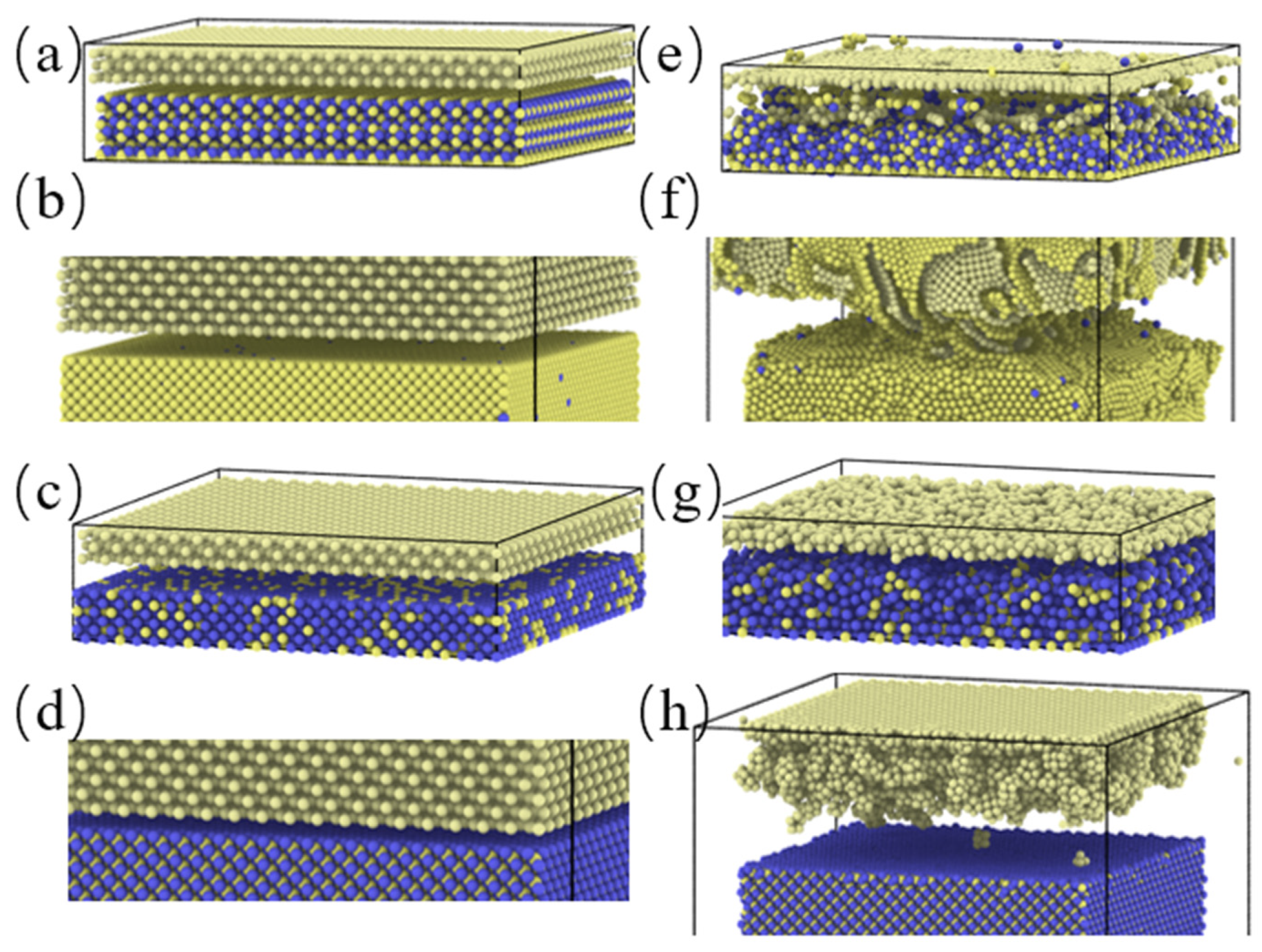
2. Model
3. Results and Discussion
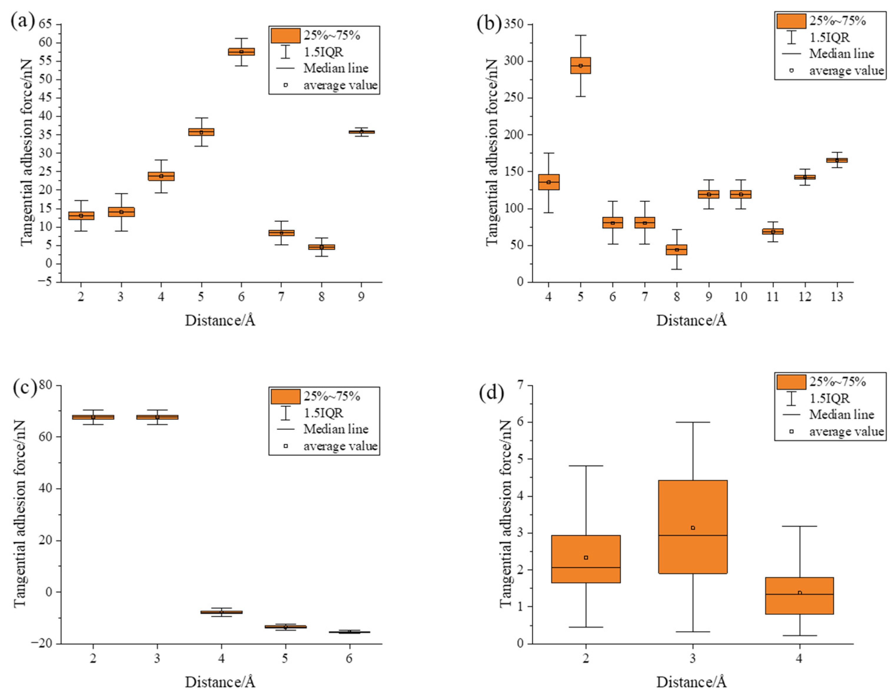
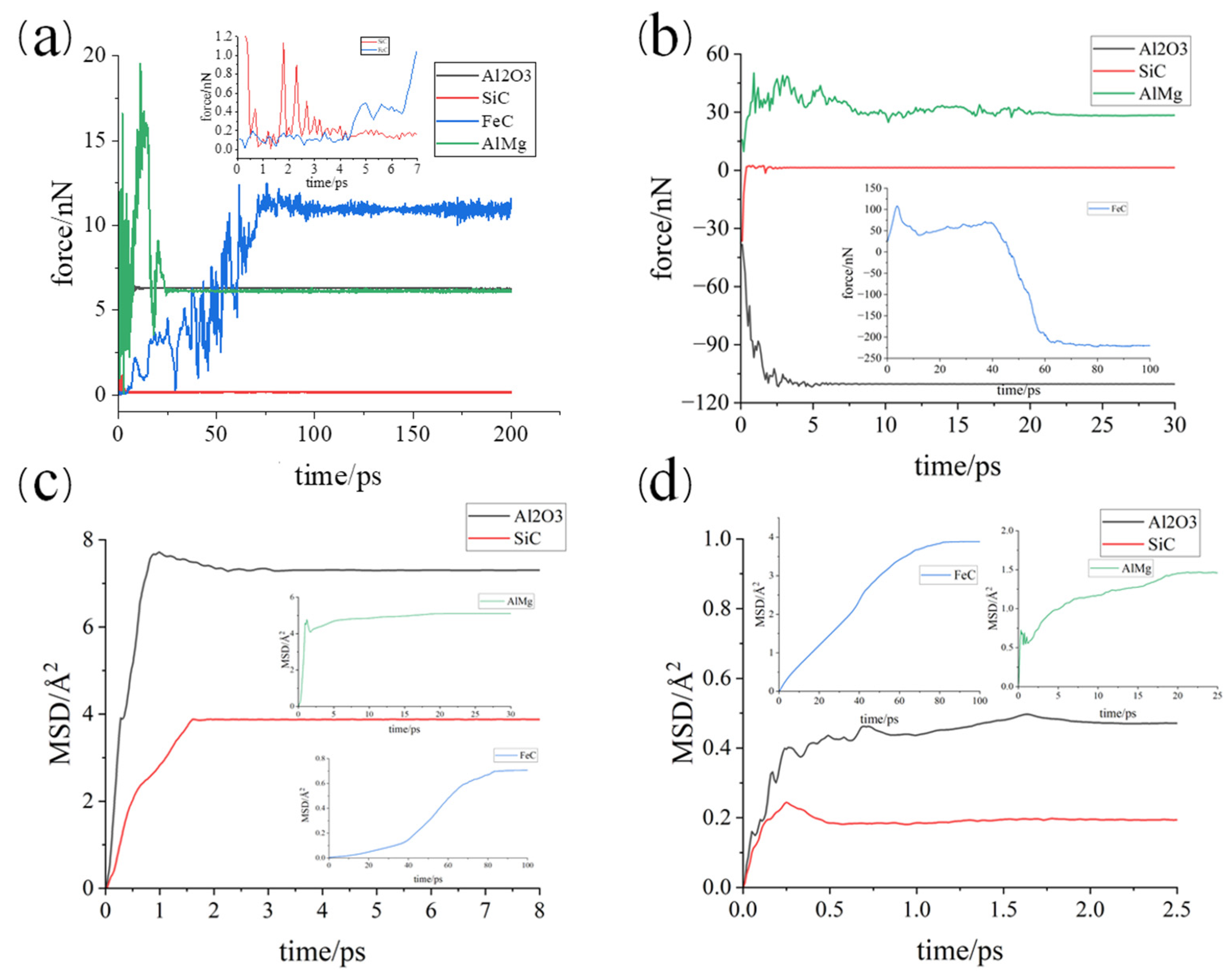
3.1. Simulation under Static Conditions
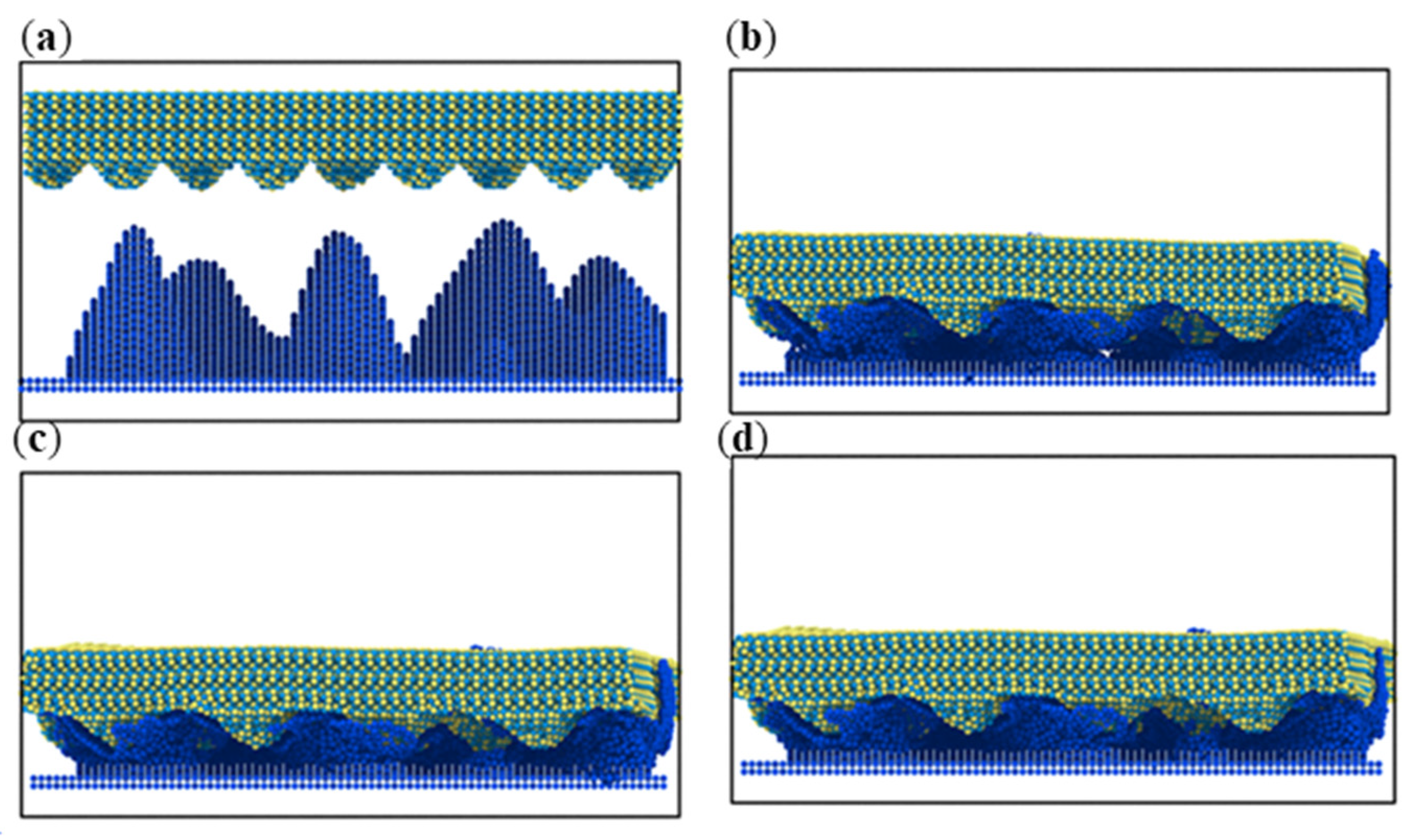
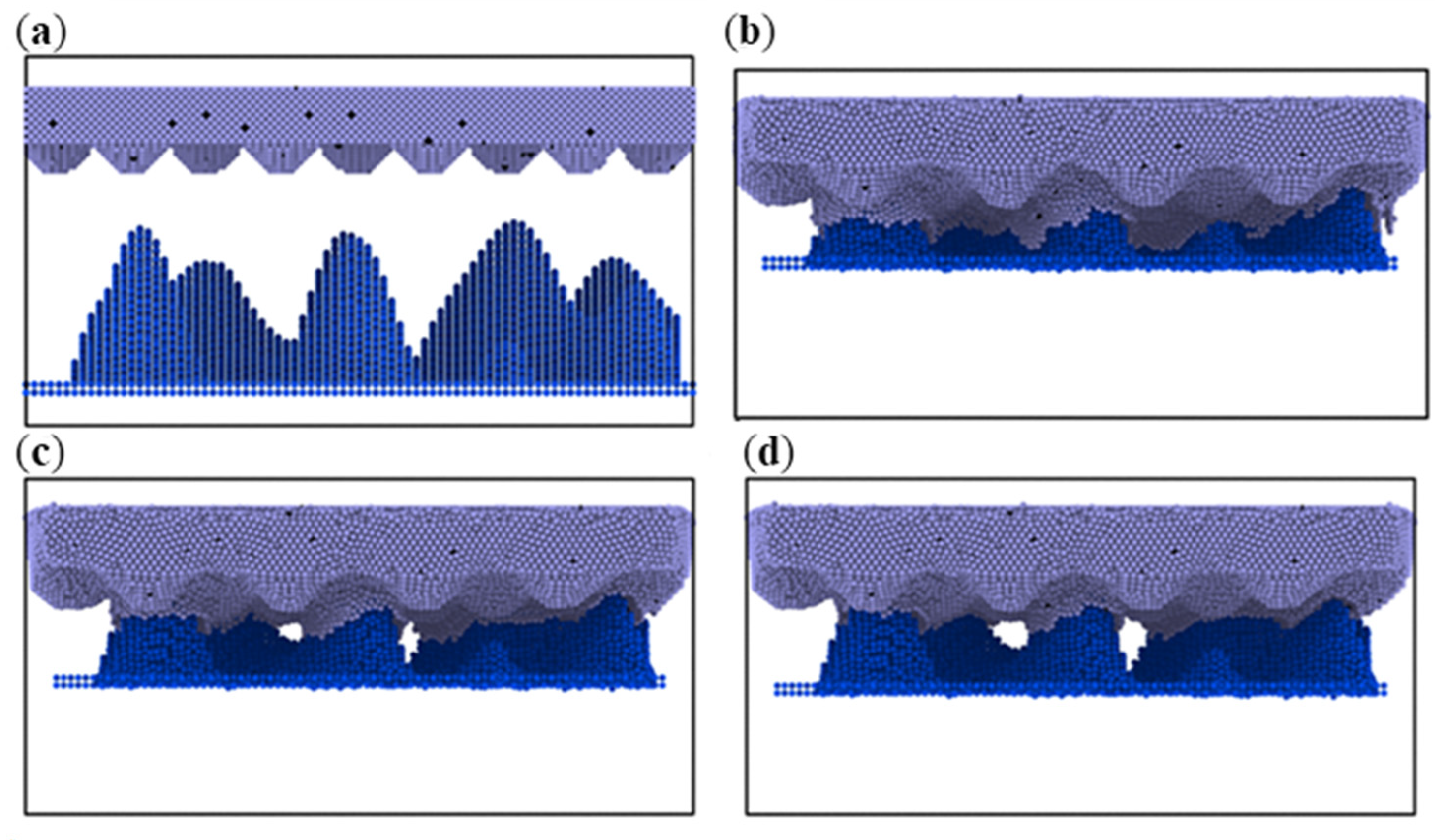
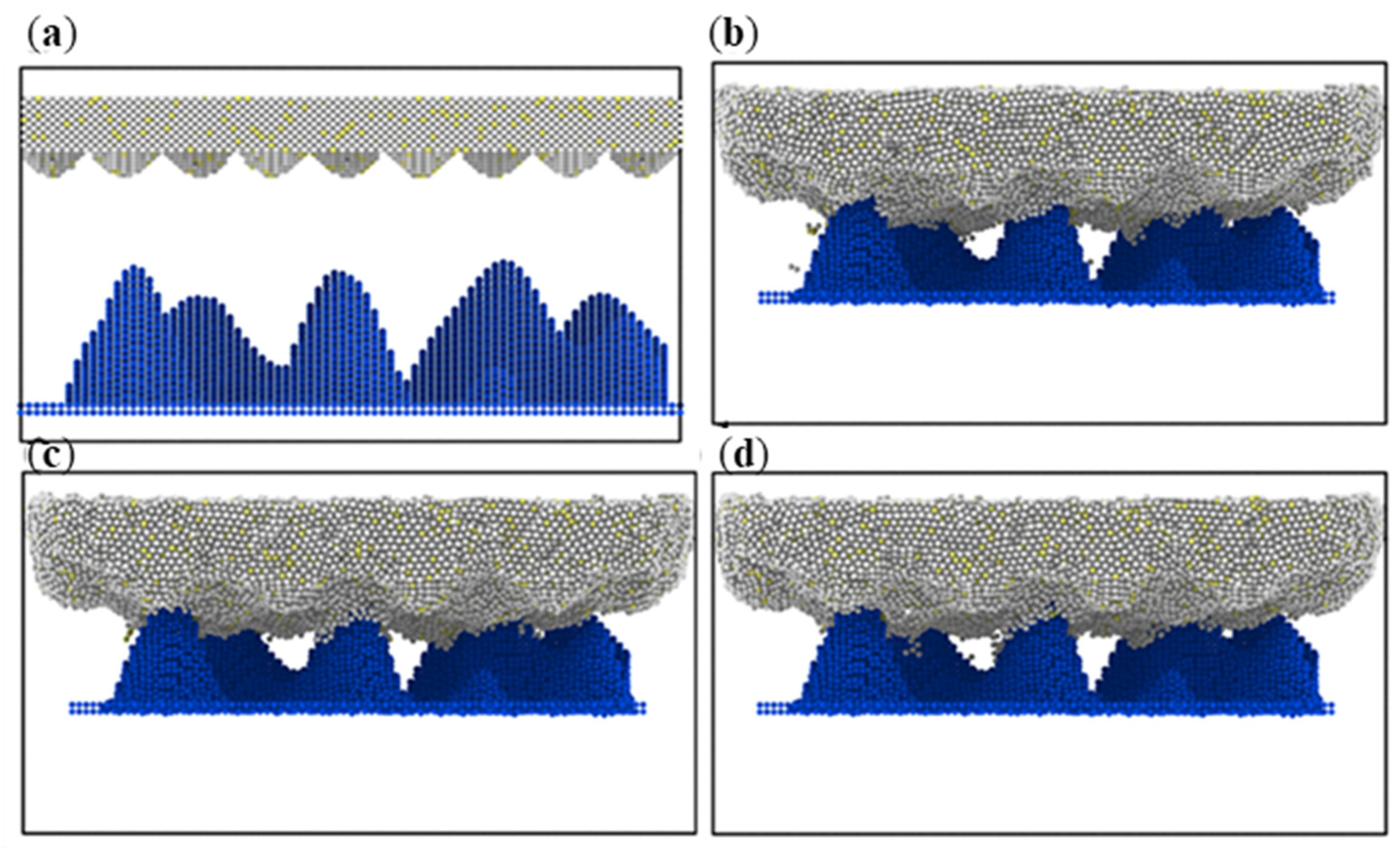
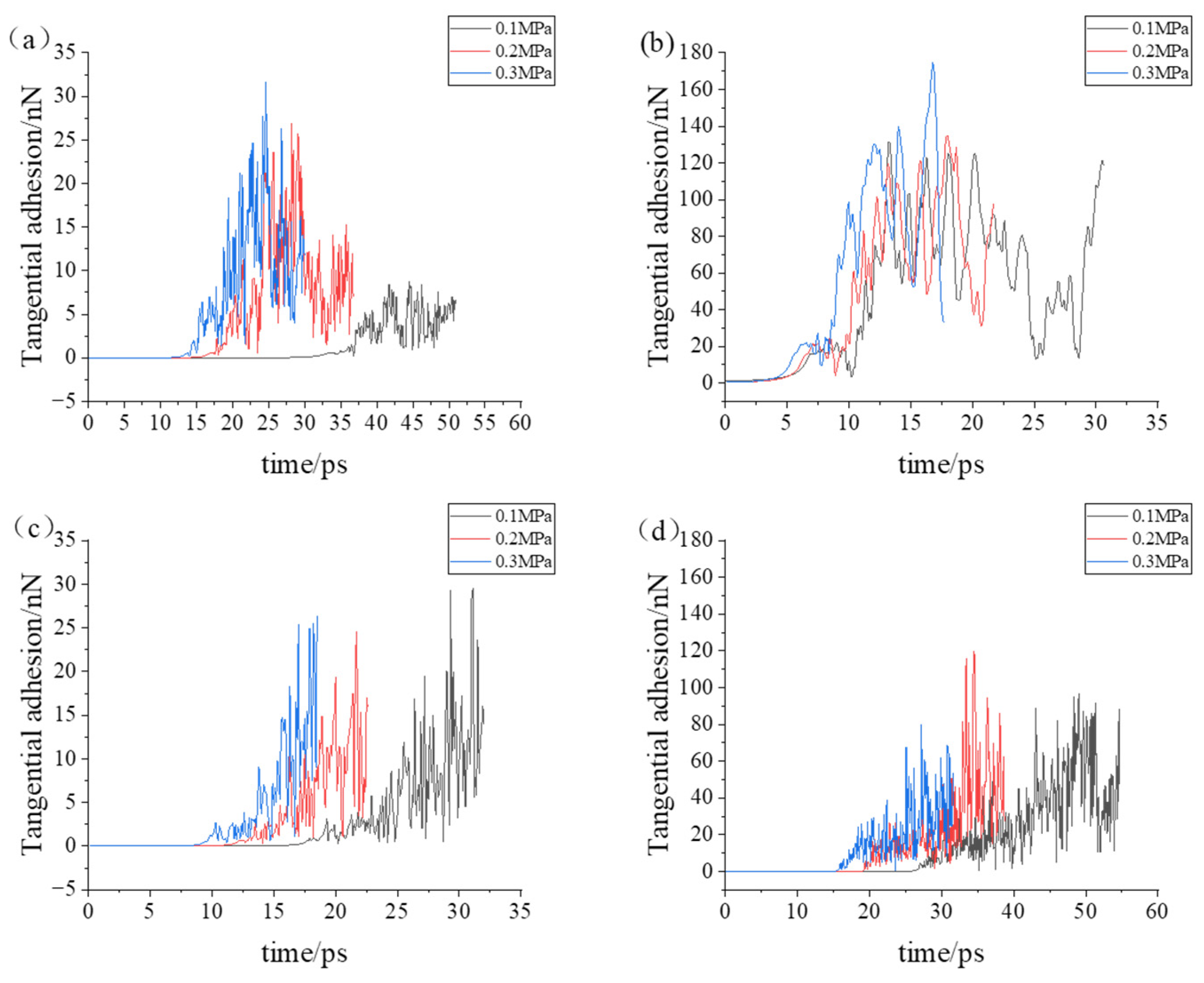
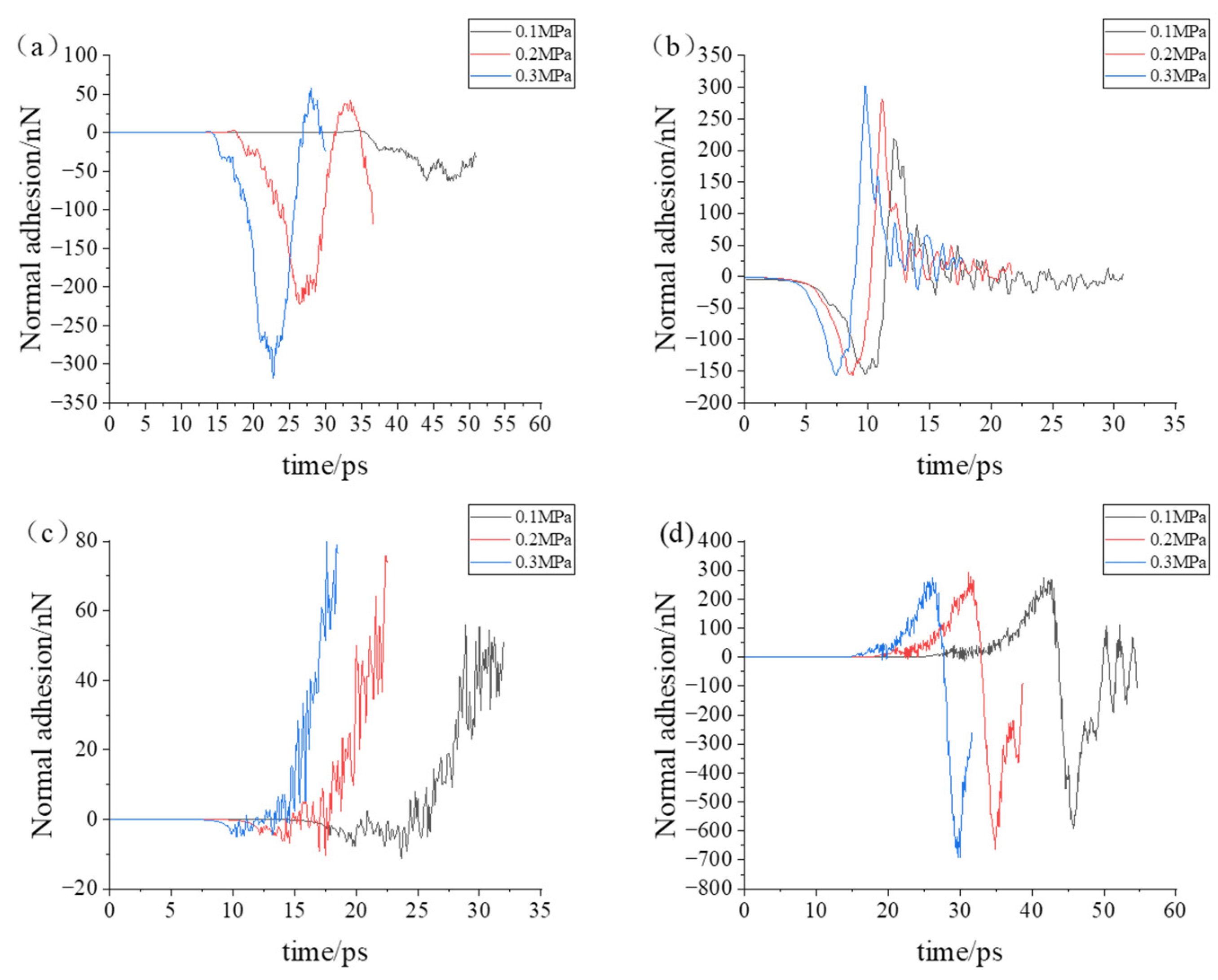
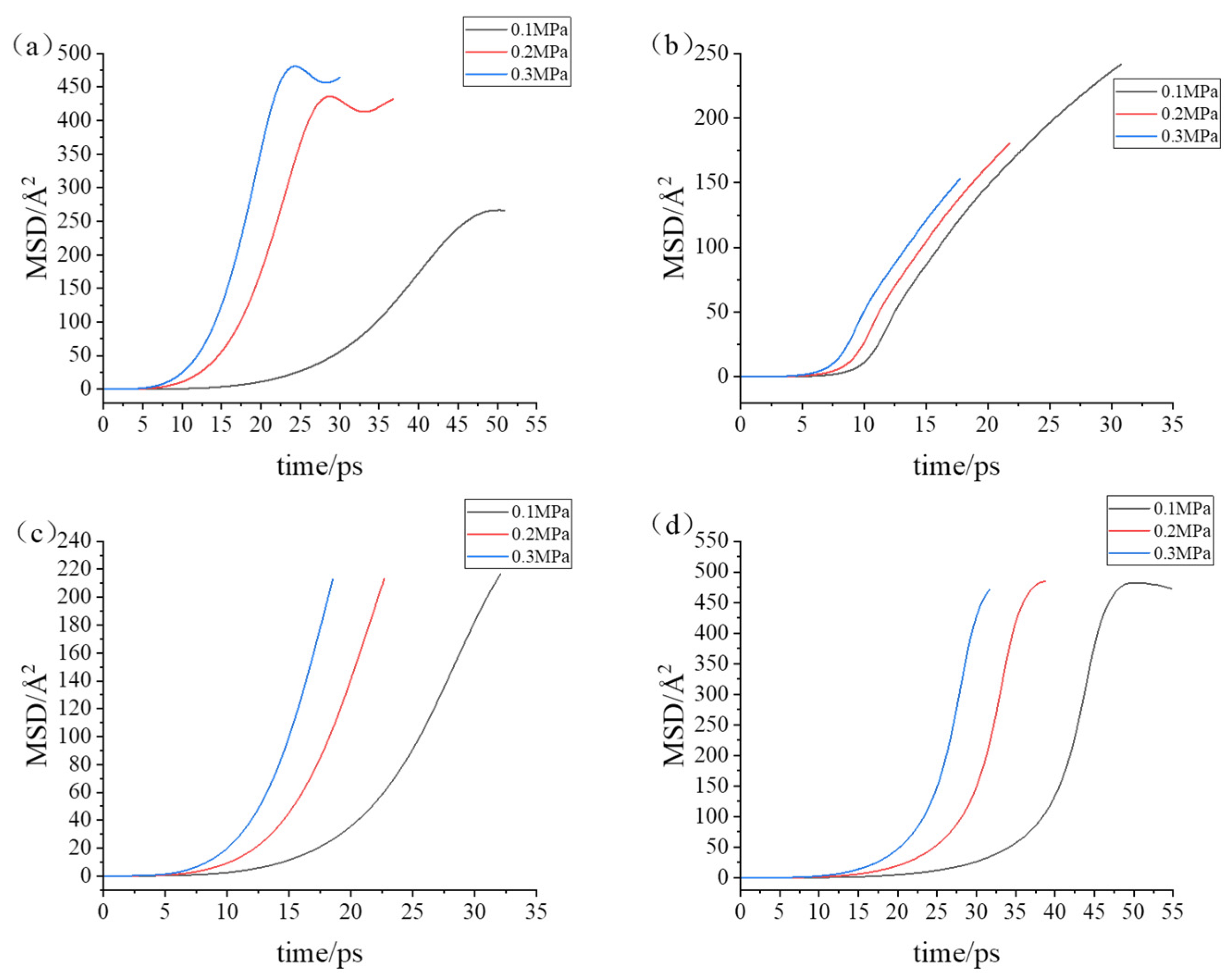
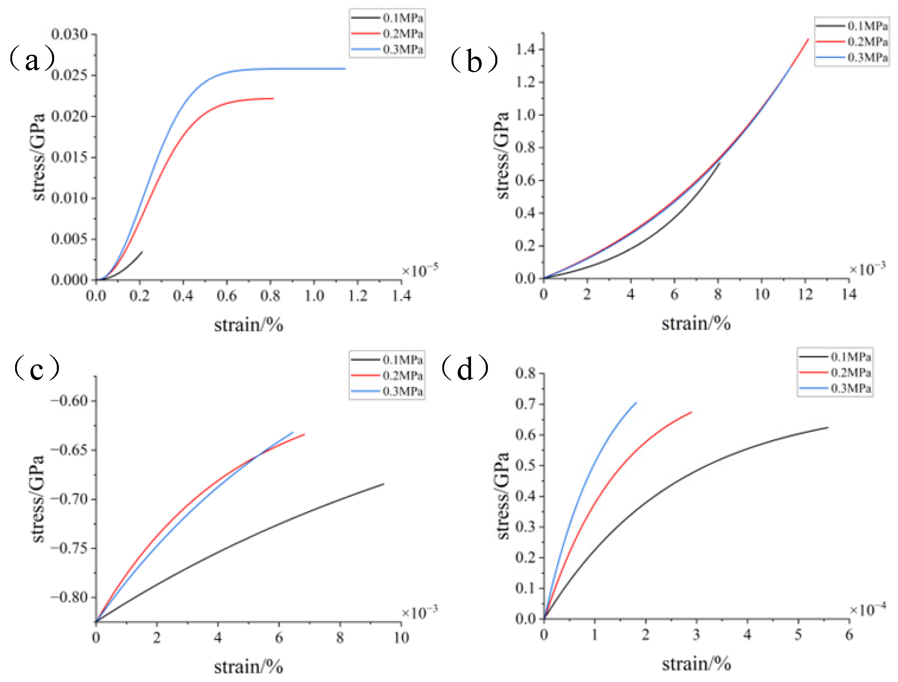
3.2. Simulation with Different Loads
4. Conclusions
- Under static conditions, the tangential adhesion force of the iron–carbon alloy and aluminum–magnesium alloy was greater than that of the aluminum oxide ceramic and silicon carbide ceramic. In the normal direction, only the aluminum–magnesium alloy exhibited an attractive force when reaching a stable state.
- During the compression simulation, the tangential adhesion force of the iron–carbon alloy was the largest, and the normal adhesion force of the aluminum–magnesium alloy was the largest.
- During compression, the aluminum–magnesium alloy and iron–carbon alloy substrates with the silicon wafer exhibited elastic deformation. The aluminum–magnesium alloy and iron-carbon alloy underwent elastic deformation, while aluminum oxide ceramic and silicon carbide ceramic substrates with the silicon wafer showed plastic deformation when compressed with the silicon carbide ceramic and elastic deformation when compressed with the aluminum oxide ceramic.
- These conclusions provide support for the construction of microarray structures to enhance adhesion, when the substrate is subjected to normal pressure, the deformation will increase the actual contact area, and at the same time, the tangential deformation can be increased, which will produce more actual contact area. At the same time, after unloading pressure, due to the elastic deformation of the substrate, the microgroove part of the microarray structure cannot contact the wafer, and the actual contact area is smaller than that without the microarray structure, which is more conducive to separating the wafer after processing.
Author Contributions
Funding
Data Availability Statement
Conflicts of Interest
References
- Stallhofer, P. Ultra-Thin Chip Technology and Applications; Joachim Burghartz; Springer: New York, NY, USA, 2011; pp. 3–12. [Google Scholar]
- Zhang, Z.; Cui, J. A novel approach of mechanical chemical grinding. J. Alloys Compd. 2017, 726, 514–524. [Google Scholar] [CrossRef]
- Dong, Z.; Lin, Y. Ultra-thin wafer technology and applications: A review. Mater. Sci. Semicond. Process 2020, 105, 104681. [Google Scholar] [CrossRef]
- Zhou, L.; Eda, H. Defect-free fabrication for single crystal silicon substrate by chemo-mechanical grinding. CIRP Ann. 2006, 55, 313–316. [Google Scholar] [CrossRef]
- Pei, Z.J.; Strasbaugh, A. Fine grinding of silicon wafers: Designed experiments. Int. J. Mach. Tools Manuf. 2002, 42, 395–404. [Google Scholar] [CrossRef]
- Pei, Z.J.; Fisher, G.R. Grinding of silicon wafers: A review from historical perspectives. Int. J. Mach. Tools Manuf. 2008, 48, 1297–1307. [Google Scholar] [CrossRef]
- Xu, L.; Chen, H. Study on rheological properties and polishing performance of viscoelastic material for dilatancy pad. Precis. Eng. 2022, 77, 328–339. [Google Scholar] [CrossRef]
- Pan, B.; Kang, R. Precision fabrication of thin copper substrate by double-sided lapping and chemical mechanical polishing. J. Manuf. Process 2019, 44, 47–54. [Google Scholar] [CrossRef]
- Hayes, A.V.; Randive, R. Evaluation of backside particle contamination and electrostatic chuck design on the cleanliness of EUV reticle mask blanks in a multilayer Mo/Si ion beam deposition system. Proc. SPIE 2008, 7122, 1169–1184. [Google Scholar]
- Une, A.; Ogasawara, N. Development of a nondeforming chucking technique for EUV lithography. Microelectron. Eng. 2013, 112, 278–281. [Google Scholar] [CrossRef]
- Yoshitomi, K.; Une, A. Study of a clamping process with no deformation for a thin substrate using a freezing pin chuck system. Precis. Eng. 2020, 64, 45–52. [Google Scholar] [CrossRef]
- Yoshitomi, K.; Une, A. Study of the Warp Removal Process for a Thin Substrate: Development of a Correction Processing System Using a Freezing Pin Chuck. Int. J. Auto. Tech-Jpn. 2020, 14, 633–643. [Google Scholar] [CrossRef]
- Zhou, H.; Xu, X.M. In Study on improved grinding process of sapphire with LED substrate material in manufacturing engineering. Adv. Mat. Res. 2012, 583, 314–317. [Google Scholar] [CrossRef]
- Xu, L.; Wang, L. Effects of pH values and H2O2 concentrations on the chemical enhanced shear dilatancy polishing of tungsten. Micromachines 2022, 13, 762. [Google Scholar] [CrossRef] [PubMed]
- Li, Z.; Pei, Z. Machining processes for sapphire wafers: A literature review. Proc. Inst. Mech. Eng. B J. Eng. Manuf. 2011, 225, 975–989. [Google Scholar] [CrossRef]
- Price, G.L.; Usher, B.F. Application of epitaxial lift-off to optoelectronic material studies. In Physical Concepts of Materials for Novel Optoelectronic Device Applications I: Materials Growth and Characterization; SPIE: Bellingham, WA, USA, 1991; p. 1361. [Google Scholar]
- Chen, Z.; Cao, L. The mechanism of layer stacked clamping (LSC) for polishing ultra-thin sapphire wafer. Micromachines 2020, 11, 759. [Google Scholar] [CrossRef] [PubMed]
- Chen, Z.; Han, S. Performance assessment of ultrathin sapphire wafer polishing with layer stacked clamping (LSC) method. Int. J. Adv. Manuf. Technol. 2023, 127, 3761–3771. [Google Scholar] [CrossRef]
- Chen, Z.; Han, S. Analysis of the Influence of the Motion State of Ultra-Thin Sapphire Based on Layer-Stacked Clamping (LSC). Micromachines 2023, 14, 1124. [Google Scholar] [CrossRef] [PubMed]
- Delrio, F.W.; Carraro, C.; Maboudian, R. Small-scale surface engineering problems. In Tribology and Dynamics of Engine and Powertrain; Woodhead Publishing: Cambridge, UK, 2010; pp. 960–989. [Google Scholar]
- Ringl, C.; Urbassek, H.M. A LAMMPS implementation of granular mechanics: Inclusion of adhesive and microscopic friction forces. Comput. Phys. Commun. 2012, 183, 986–992. [Google Scholar] [CrossRef]
- Stukowski, A. Visualization and analysis of atomistic simulation data with OVITO–the Open Visualization Tool. Model. Simul. Mat. Sci. Eng. 2009, 18, 015012. [Google Scholar] [CrossRef]
- Tersoff, J. New empirical approach for the structure and energy of covalent systems. Phys. Rev. B 1988, 37, 6991. [Google Scholar] [CrossRef]
- Tersoff, J. Chemical order in amorphous silicon carbide. Phys. Rev. B 1994, 49, 16349. [Google Scholar] [CrossRef] [PubMed]
- Choudhary, K.; Liang, T. Charge optimized many-body (COMB) potential for Al2O3 materials, interfaces, and nanostructures. J. Phys. Condens. Matter 2015, 27, 305004. [Google Scholar] [CrossRef]
- Lee, B.J. A modified embedded-atom method interatomic potential for the Fe–C system. Acta Mater. 2006, 54, 701–711. [Google Scholar] [CrossRef]
- Mendelev, M.I.; Asta, M. Development of interatomic potentials appropriate for simulation of solid–liquid interface properties in Al–Mg alloys. Philos. Mag. 2009, 89, 3269–3285. [Google Scholar] [CrossRef]
- Rappé, A.K.; Casewit, C.J. UFF, a full periodic table force field for molecular mechanics and molecular dynamics simulations. J. Am. Chem. Soc. 1992, 114, 10024–10035. [Google Scholar] [CrossRef]
- Mayo, S.L.; Olafson, B.D. DREIDING: A generic force field for molecular simulations. J. Phys. Chem. C 1990, 94, 8897–8909. [Google Scholar] [CrossRef]


| Atom | (Å) | (kcal/mol) |
|---|---|---|
| Al | 4.499 | 0.505 |
| O | 3.541 | 0.195 |
| Si | 4.27 | 0.31 |
| Fe | 4.54 | 0.055 |
| Mg | 2.96 | 0.111 |
| C | 3.4 | 0.0556 |
Disclaimer/Publisher’s Note: The statements, opinions and data contained in all publications are solely those of the individual author(s) and contributor(s) and not of MDPI and/or the editor(s). MDPI and/or the editor(s) disclaim responsibility for any injury to people or property resulting from any ideas, methods, instructions or products referred to in the content. |
© 2024 by the authors. Licensee MDPI, Basel, Switzerland. This article is an open access article distributed under the terms and conditions of the Creative Commons Attribution (CC BY) license (https://creativecommons.org/licenses/by/4.0/).
Share and Cite
Han, S.; Chen, Y.; Feng, M.; Zhang, Z.; Wang, Z.; Chen, Z. Molecular Dynamics Analysis of Adhesive Forces between Silicon Wafer and Substrate in Microarray Adhesion. Lubricants 2024, 12, 183. https://doi.org/10.3390/lubricants12060183
Han S, Chen Y, Feng M, Zhang Z, Wang Z, Chen Z. Molecular Dynamics Analysis of Adhesive Forces between Silicon Wafer and Substrate in Microarray Adhesion. Lubricants. 2024; 12(6):183. https://doi.org/10.3390/lubricants12060183
Chicago/Turabian StyleHan, Shunkai, Yarong Chen, Ming Feng, Zhixu Zhang, Zhaopei Wang, and Zhixiang Chen. 2024. "Molecular Dynamics Analysis of Adhesive Forces between Silicon Wafer and Substrate in Microarray Adhesion" Lubricants 12, no. 6: 183. https://doi.org/10.3390/lubricants12060183
APA StyleHan, S., Chen, Y., Feng, M., Zhang, Z., Wang, Z., & Chen, Z. (2024). Molecular Dynamics Analysis of Adhesive Forces between Silicon Wafer and Substrate in Microarray Adhesion. Lubricants, 12(6), 183. https://doi.org/10.3390/lubricants12060183