Graphene Field Effect Transistors for Biomedical Applications: Current Status and Future Prospects


Abstract
:
1. Introduction
2. Graphene Platform
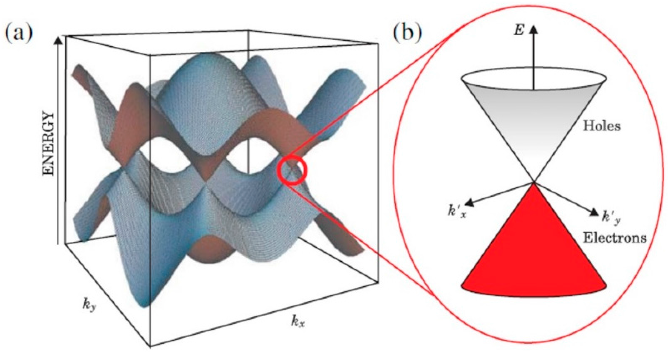
2.1. Graphene Properties
2.2. G-FET Development
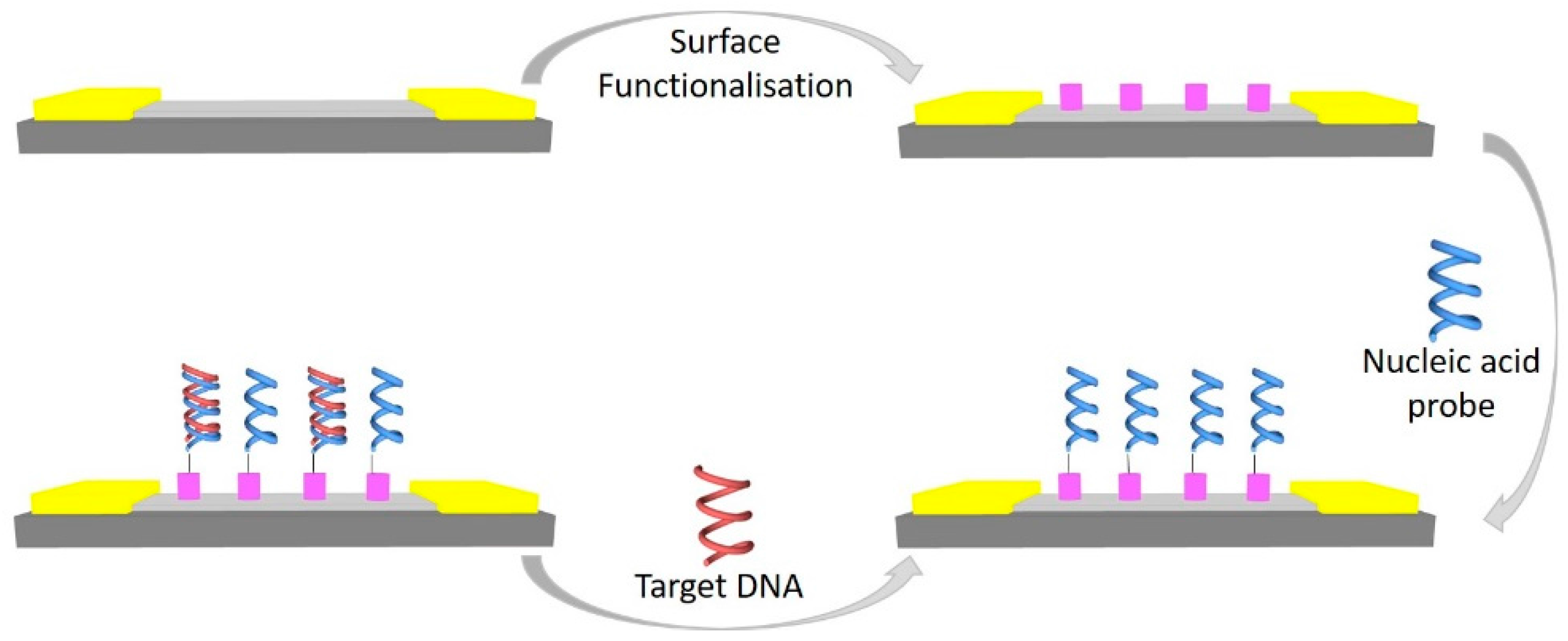
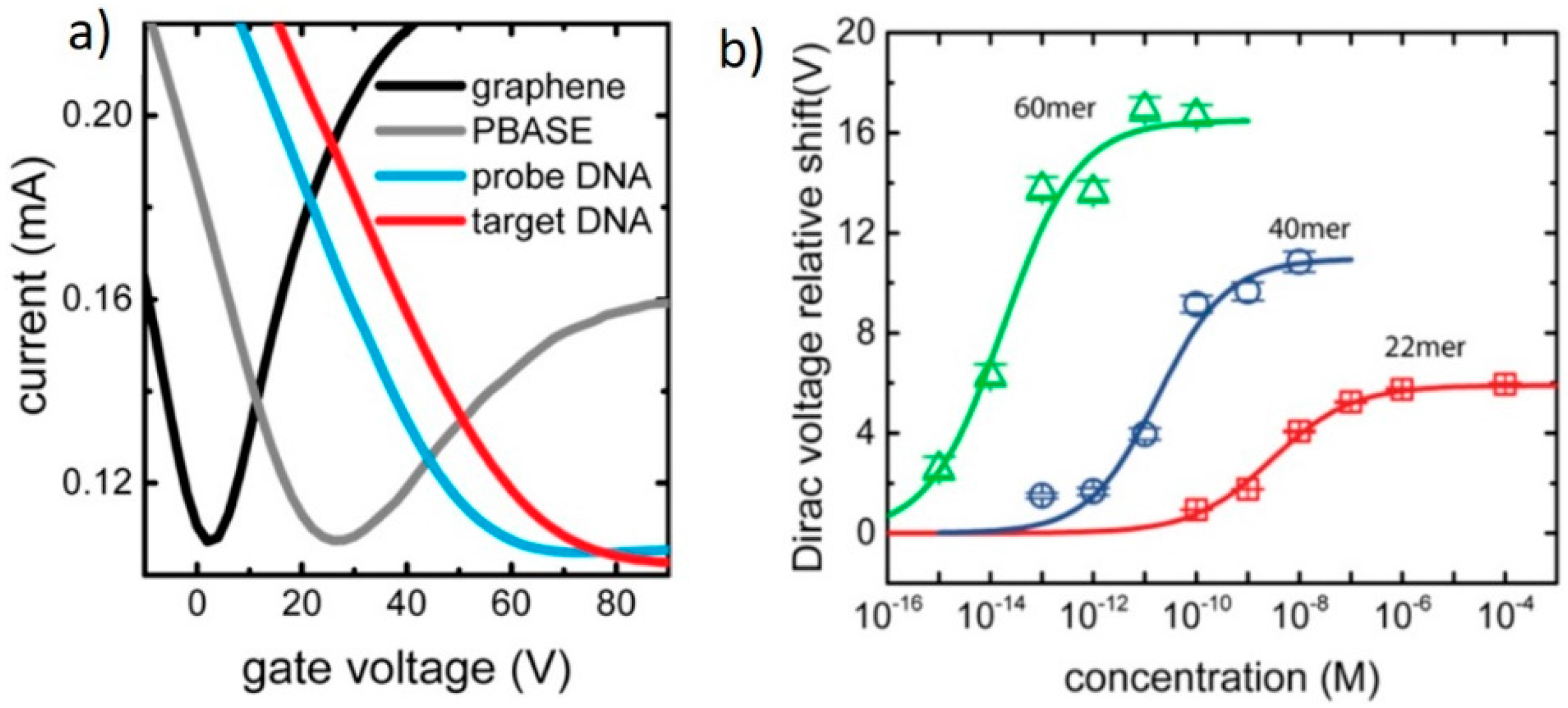
3. G-FET-Based Nucleic Acid Sensors
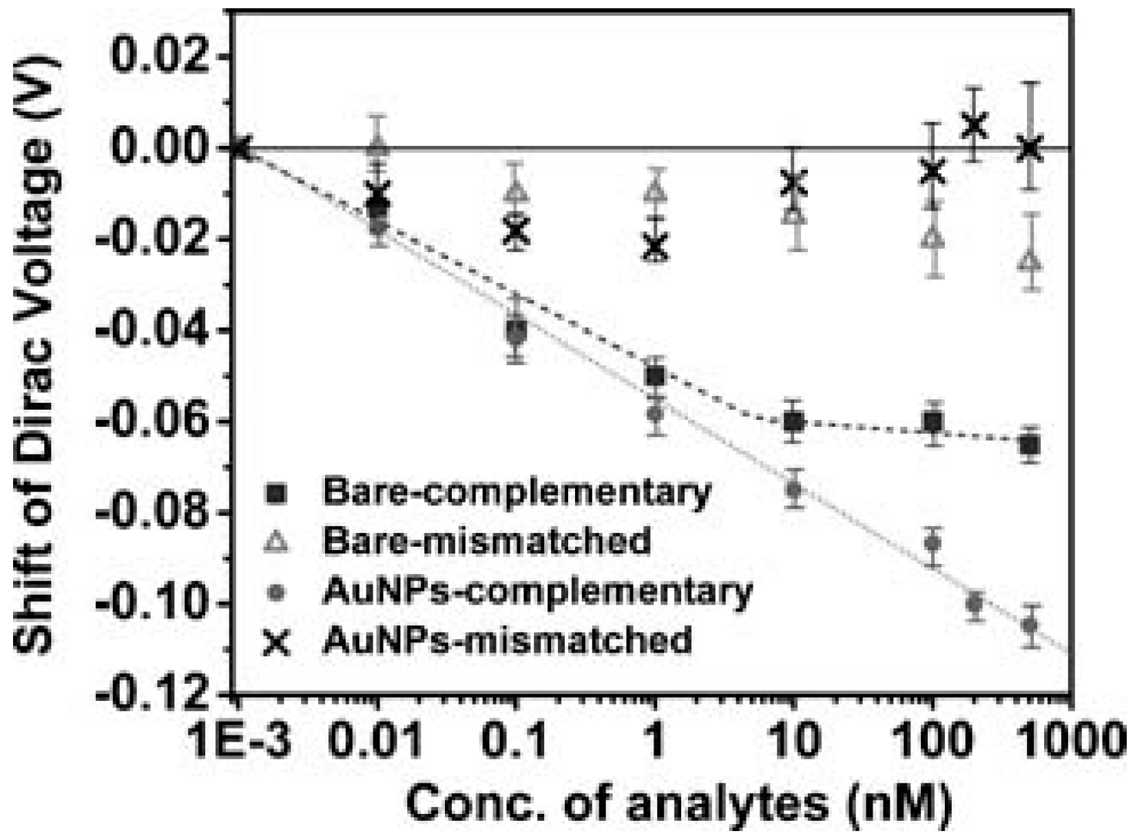
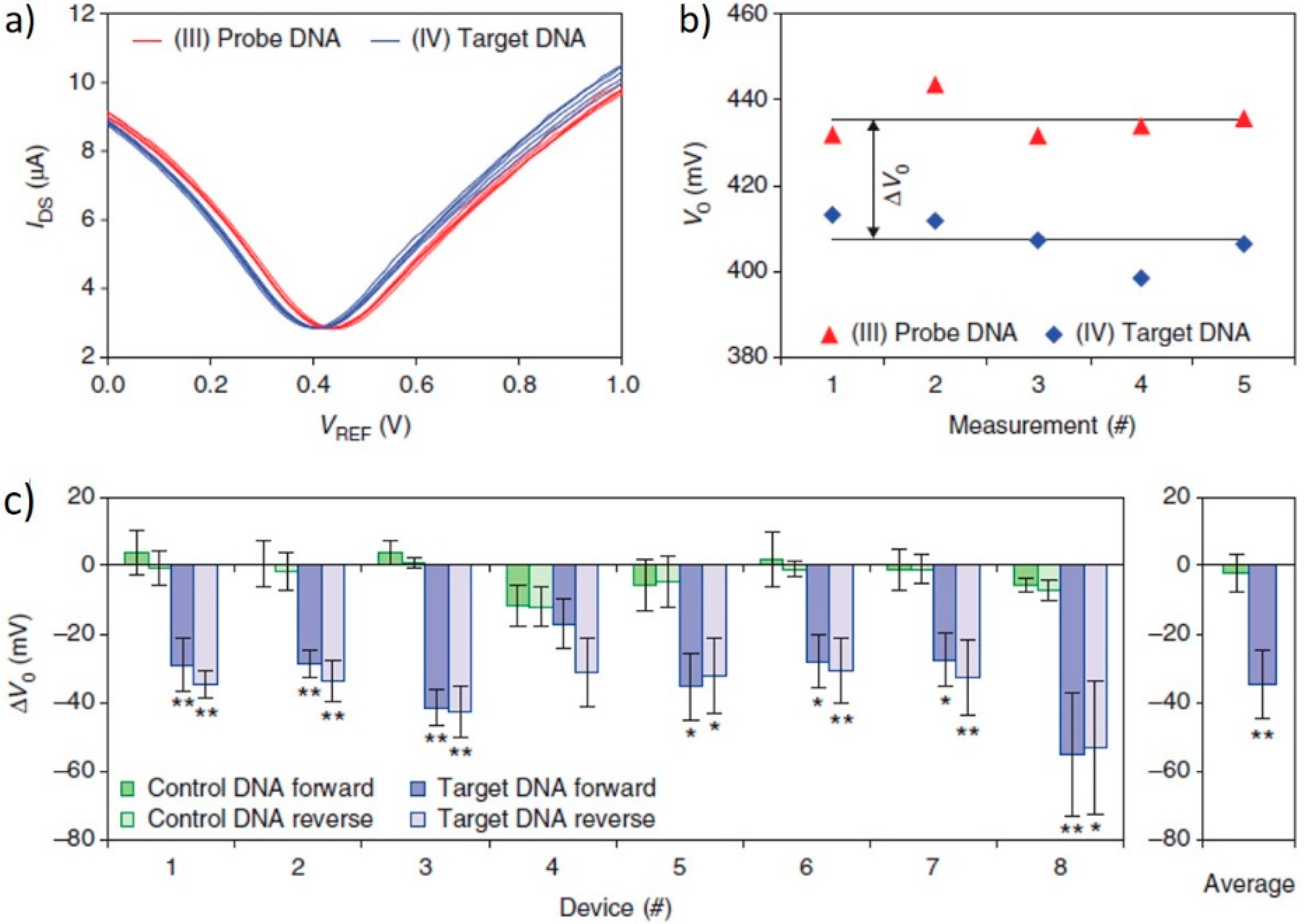
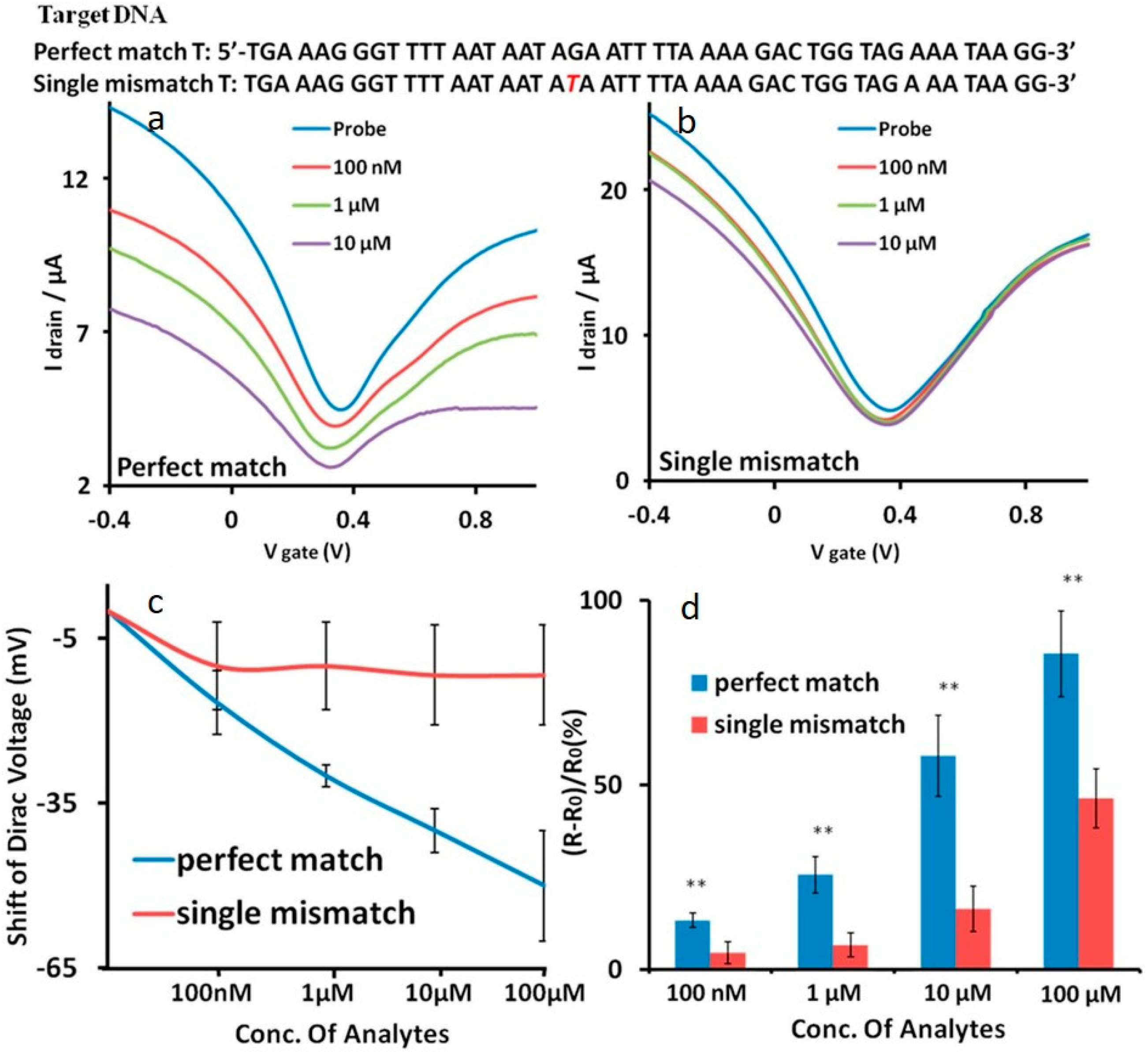
3.1. DNA Sensor
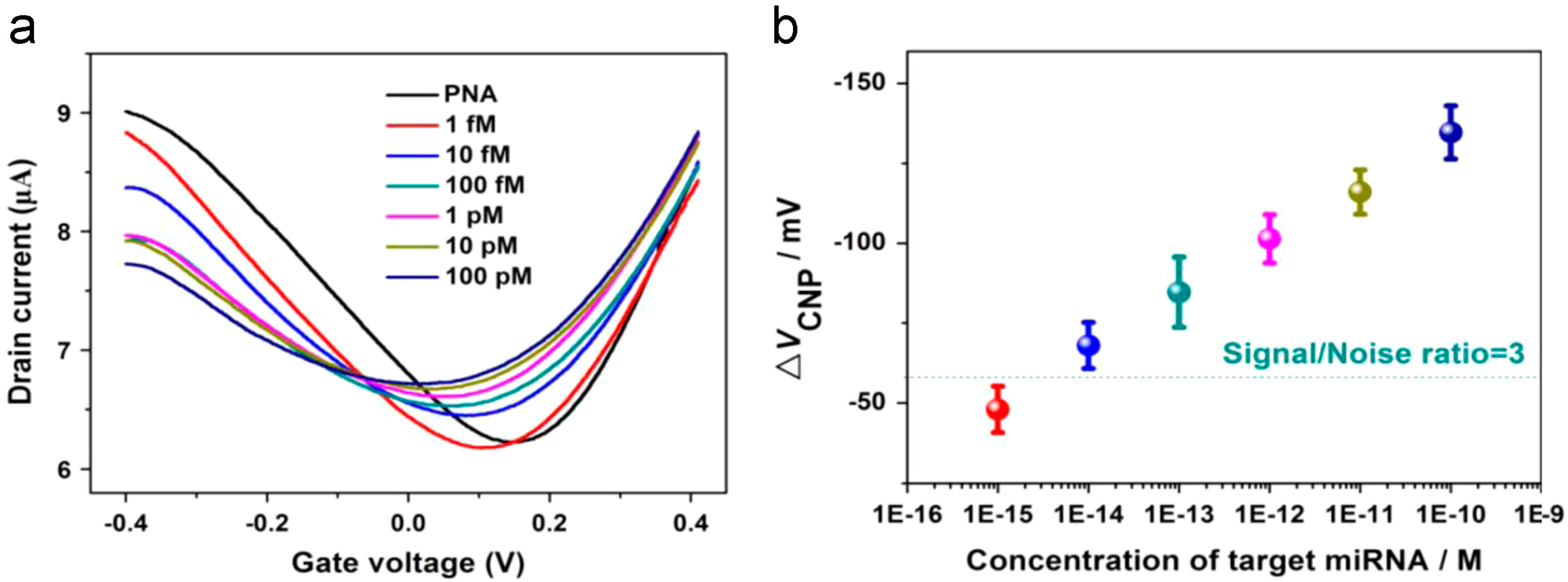
3.2. miRNA Sensor
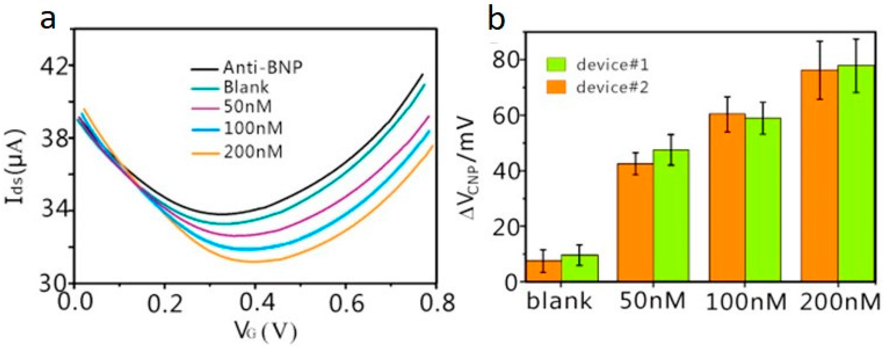
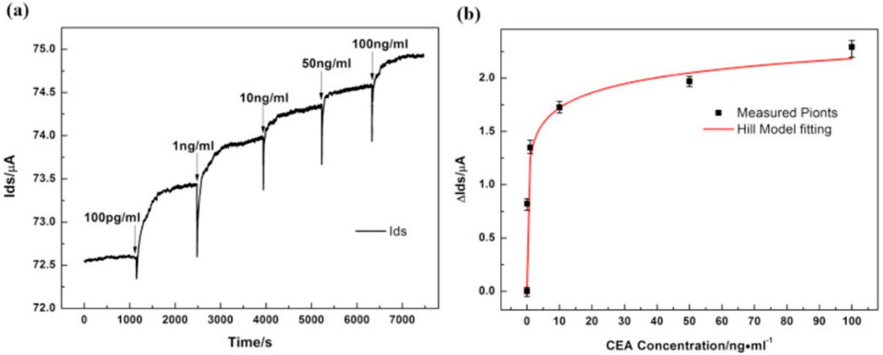
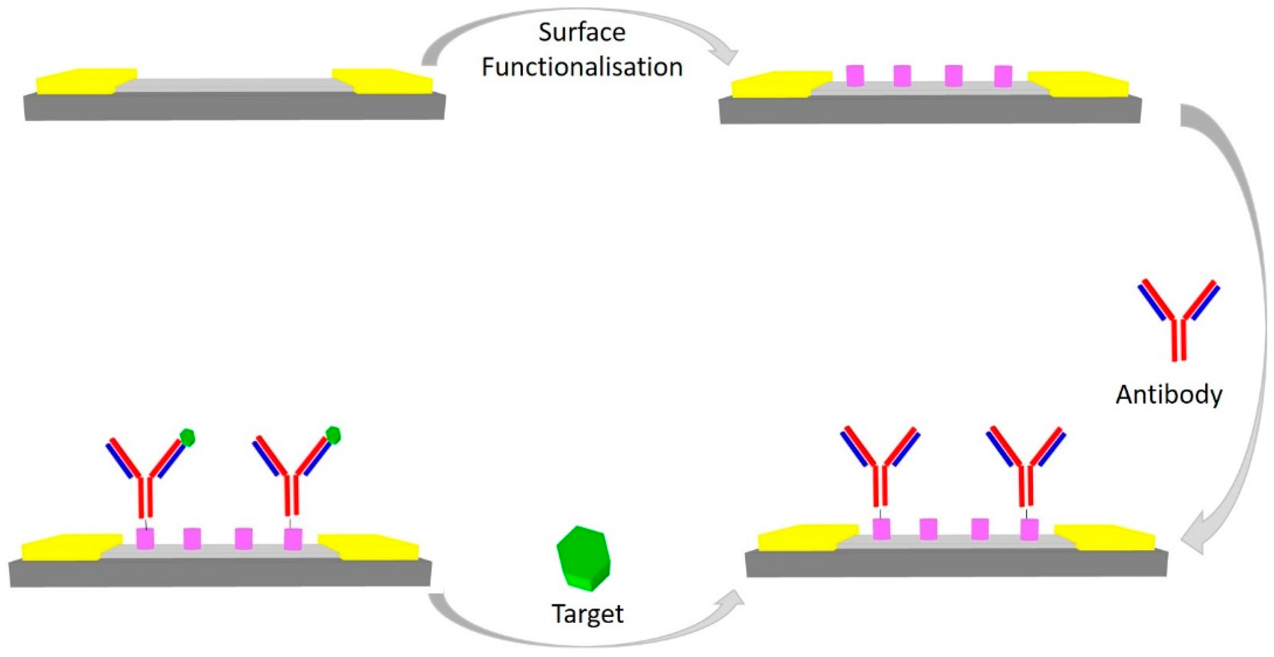
4. Immunosensors
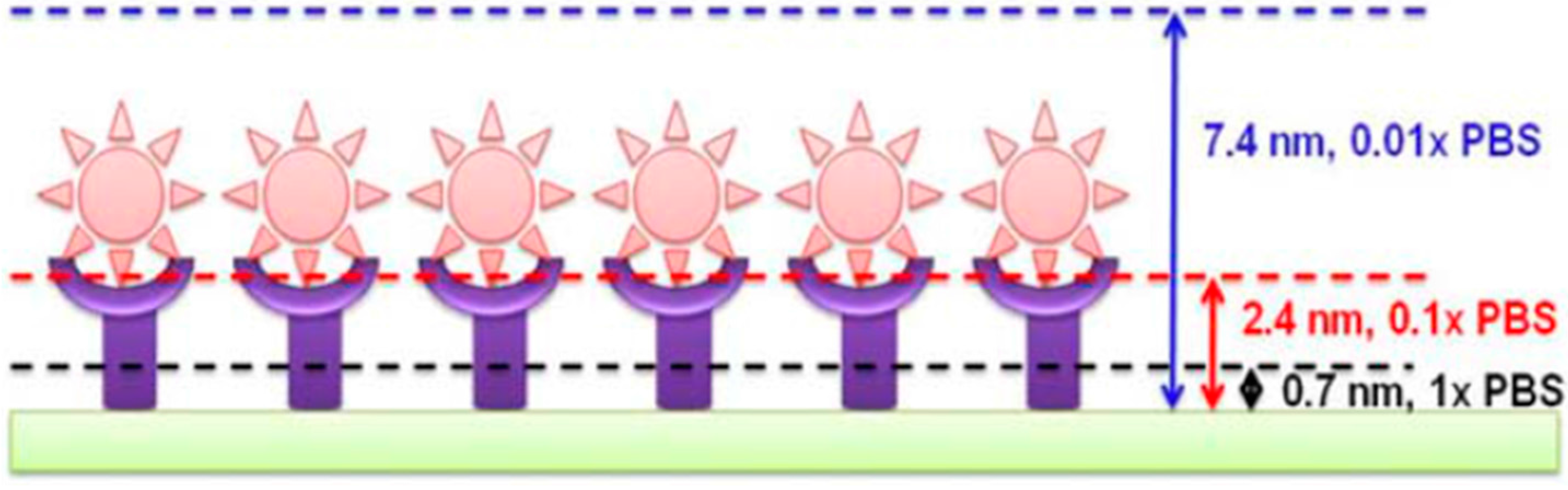
Debye–Hükel Screening
5. Current Challenges and Future Prospects
Acknowledgments
Conflicts of Interest
References
- Novoselov, K.S.; Geim, A.K.; Morozov, S.V.; Jiang, D.; Zhang, Y.; Dubonos, S.V.; Grigorieva, I.V.; Firsov, A.A. Electric field effect in atomically thin carbon films. Science 2004, 306, 666–669. [Google Scholar] [CrossRef] [PubMed]
- Kuila, T.; Bose, S.; Khanra, P.; Mishra, A.K.; Kim, N.H.; Lee, J.H. Recent advances in graphene-based biosensors. Biosens. Bioelectron. 2011, 26, 4637–4648. [Google Scholar] [CrossRef] [PubMed]
- Ali Tahir, A.; Ullah, H.; Sudhagar, P.; Asri Mat Teridi, M.; Devadoss, A.; Sundaram, S. The application of graphene and its derivatives to energy conversion, storage, and environmental and biosensing devices. Chem. Rec. 2016, 16, 1591–1634. [Google Scholar] [CrossRef] [PubMed]
- Clark, L.C., Jr.; Lyons, C. Electrode systems for continuous monitoring in cardiovascular surgery. Ann. N. Y. Acad. Sci. 1962, 102, 29–45. [Google Scholar] [CrossRef] [PubMed]
- Wang, J. Glucose biosensors: 40 years of advances and challenges. Sens. Update 2002, 10, 107–119. [Google Scholar] [CrossRef]
- Yang, Y.; Pan, J.Y.; Hua, W.J.; Tu, Y.F. An approach for the preparation of highly sensitive electrochemical impedimetric immunosensors for the detection of illicit drugs. J. Electroanal. Chem. 2014, 726, 1–6. [Google Scholar] [CrossRef]
- Cui, Y.; Wei, Q.; Park, H.; Lieber, C.M. Nanowire nanosensors for highly sensitive and selective detection of biological and chemical species. Science 2001, 293, 1289. [Google Scholar] [CrossRef] [PubMed]
- Zheng, G.; Patolsky, F.; Cui, Y.; Wang, W.U.; Lieber, C.M. Multiplexed electrical detection of cancer markers with nanowire sensor arrays. Nat. Biotechnol. 2005, 23, 1294–1301. [Google Scholar] [CrossRef] [PubMed]
- Chua, J.H.; Chee, R.-E.; Agarwal, A.; Wong, S.M.; Zhang, G.-J. Label-free electrical detection of cardiac biomarker with complementary metal-oxide semiconductor-compatible silicon nanowire sensor arrays. Anal. Chem. 2009, 81, 6266–6271. [Google Scholar] [CrossRef] [PubMed]
- Hahm, J.-I.; Lieber, C.M. Direct ultrasensitive electrical detection of DNA and DNA sequence variations using nanowire nanosensors. Nano Lett. 2004, 4, 51–54. [Google Scholar] [CrossRef]
- Allen, B.L.; Kichambare, P.D.; Star, A. Carbon nanotube field-effect-transistor-based biosensors. Adv. Mater. 2007, 19, 1439–1451. [Google Scholar] [CrossRef]
- Kauffman, D.R.; Star, A. Electronically monitoring biological interactions with carbon nanotube field-effect transistors. Chem. Soc. Rev. 2008, 37, 1197–1206. [Google Scholar] [CrossRef] [PubMed]
- Liu, S.; Guo, X. Carbon nanomaterials field-effect-transistor-based biosensors. NPG Asia Mater. 2012, 4, 23. [Google Scholar] [CrossRef]
- Zhou, W.Z.; Huang, P.J.J.; Ding, J.S.; Liu, J. Aptamer-based biosensors for biomedical diagnostics. Analyst 2014, 139, 2627–2640. [Google Scholar] [CrossRef] [PubMed]
- Bolotin, K.I.; Sikes, K.J.; Jiang, Z.; Klima, M.; Fudenberg, G.; Hone, J.; Kim, P.; Stormer, H.L. Ultrahigh electron mobility in suspended graphene. Solid State Commun. 2008, 146, 351–355. [Google Scholar] [CrossRef]
- Matsumoto, K.; Maehashi, K.; Ohno, Y.; Inoue, K. Recent advances in functional graphene biosensors. J. Phys. D Appl. Phys. 2014, 47, 6. [Google Scholar] [CrossRef]
- Chen, K.I.; Li, B.R.; Chen, Y.T. Silicon nanowire field-effect transistor-based biosensors for biomedical diagnosis and cellular recording investigation. Nano Today 2011, 6, 131–154. [Google Scholar] [CrossRef]
- Chen, L.P.; Wang, L.J.; Shuai, Z.G.; Beljonne, D. Energy level alignment and charge carrier mobility in noncovalently functionalized graphene. J. Phys. Chem. Lett. 2013, 4, 2158–2165. [Google Scholar] [CrossRef]
- Huang, P.; Jing, L.; Zhu, H.R.; Gao, X.Y. Diazonium functionalized graphene: Microstructure, electric, and magnetic properties. Acc. Chem. Res. 2013, 46, 43–52. [Google Scholar] [CrossRef] [PubMed]
- Liu, M.C.; Duan, Y.X.; Wang, Y.; Zhao, Y. Diazonium functionalization of graphene nanosheets and impact response of aniline modified graphene/bismaleimide nanocomposites. Mater. Des. 2014, 53, 466–474. [Google Scholar] [CrossRef]
- Wang, J.Y.; Zhao, R.Q.; Yang, M.M.; Liu, Z.F.; Liu, Z.R. Inverse relationship between carrier mobility and bandgap in graphene. J. Chem. Phys. 2013, 138, 5. [Google Scholar] [CrossRef] [PubMed]
- Deokar, G.; Avila, J.; Razado-Colambo, I.; Codron, J.L.; Boyaval, C.; Galopin, E.; Asensio, M.C.; Vignaud, D. Towards high quality CVD graphene growth and transfer. Carbon 2015, 89, 82–92. [Google Scholar] [CrossRef]
- Das Sarma, S.; Adam, S.; Hwang, E.H.; Rossi, E. Electronic transport in two-dimensional graphene. Rev. Mod. Phys. 2011, 83, 407–470. [Google Scholar] [CrossRef]
- Gao, N.; Gao, T.; Yang, X.; Dai, X.C.; Zhou, W.; Zhang, A.Q.; Lieber, C.M. Specific detection of biomolecules in physiological solutions using graphene transistor biosensors. Proc. Natl. Acad. Sci. USA 2016, 113, 14633–14638. [Google Scholar] [CrossRef] [PubMed]
- Ping, J.L.; Vishnubhotla, R.; Vrudhula, A.; Johnson, A.T.C. Scalable production of high-sensitivity, label-free dna biosensors based on back-gated graphene field effect transistors. ACS Nano 2016, 10, 8700–8704. [Google Scholar] [CrossRef] [PubMed]
- Wang, Y.; Li, Z.H.; Wang, J.; Li, J.H.; Lin, Y.H. Graphene and graphene oxide: Biofunctionalization and applications in biotechnology. Trends Biotechnol. 2011, 29, 205–212. [Google Scholar] [CrossRef] [PubMed]
- Guy, O.J.; Walker, K.-A.D. Graphene functionalization for biosensor applications. In Silicon Carbide Biotechnology: A Biocompatible Semiconductor for Advanced Biomedical Devices and Applications; Elsevier: Amsterdam, The Netherlands, 2016; pp. 109–120. [Google Scholar]
- Mao, H.Y.; Lu, Y.H.; Lin, J.D.; Zhong, S.; Wee, A.T.S.; Chen, W. Manipulating the electronic and chemical properties of graphene via molecular functionalization. Prog. Surf. Sci. 2013, 88, 132–159. [Google Scholar] [CrossRef]
- Chen, M.J.; Zhou, H.Q.; Qiu, C.Y.; Yang, H.C.; Yu, F.; Sun, L.F. Layer-dependent fluorination and doping of graphene via plasma treatment. Nanotechnology 2012, 23, 6. [Google Scholar] [CrossRef] [PubMed]
- Jaiswal, M.; Lim, C.; Bao, Q.L.; Toh, C.T.; Loh, K.P.; Ozyilmaz, B. Controlled hydrogenation of graphene sheets and nanoribbons. ACS Nano 2011, 5, 888–896. [Google Scholar] [CrossRef] [PubMed]
- Georgakilas, V.; Otyepka, M.; Bourlinos, A.B.; Chandra, V.; Kim, N.; Kemp, K.C.; Hobza, P.; Zboril, R.; Kim, K.S. Functionalization of graphene: Covalent and non-covalent approaches, derivatives and applications. Chem. Rev. 2012, 112, 6156–6214. [Google Scholar] [CrossRef] [PubMed]
- Tehrani, Z.; Guy, O.J.; Castaing, A.; Doak, S.H. Detection of monoclonal antibodies using chemically modified graphite substrates. IEEE Sens. 2010, 2010, 428–431. [Google Scholar]
- Teixeira, S.; Burwell, G.; Castaing, A.; Gonzalez, D.; Conlan, R.S.; Guy, O.J. Epitaxial graphene immunosensor for human chorionic gonadotropin. Sens. Actuators B Chem. 2014, 190, 723–729. [Google Scholar] [CrossRef]
- Tehrani, Z.; Burwell, G.; Azmi, M.A.M.; Castaing, A.; Rickman, R.; Almarashi, J.; Dunstan, P.; Beigi, A.M.; Doak, S.H.; Guy, O.J. Generic epitaxial graphene biosensors for ultrasensitive detection of cancer risk biomarker. 2D Mater. 2014, 1, 19. [Google Scholar] [CrossRef]
- Lonkar, S.P.; Deshmukh, Y.S.; Abdala, A.A. Recent advances in chemical modifications of graphene. Nano Res. 2015, 8, 1039–1074. [Google Scholar] [CrossRef]
- Saltzgaber, G.; Wojcik, P.; Sharf, T.; Leyden, M.R.; Wardini, J.L.; Heist, C.A.; Adenuga, A.A.; Remcho, V.T.; Minot, E.D. Scalable graphene field-effect sensors for specific protein detection. Nanotechnology 2013, 24, 5. [Google Scholar] [CrossRef] [PubMed]
- Xu, S.C.; Zhan, J.; Man, B.Y.; Jiang, S.Z.; Yue, W.W.; Gao, S.B.; Guo, C.; Liu, H.; Li, Z.; Wang, J.; et al. Real-time reliable determination of binding kinetics of DNA hybridization using a multi-channel graphene biosensor. Nat. Commun. 2017, 8, 10. [Google Scholar] [CrossRef] [PubMed]
- Hwang, M.T.; Landon, P.B.; Lee, J.; Choi, D.; Mo, A.H.; Glinsky, G.; Lal, R. Highly specific SNP detection using 2D graphene electronics and DNA strand displacement. Proc. Natl. Acad. Sci. USA 2016, 113, 7088–7093. [Google Scholar] [CrossRef] [PubMed]
- Zheng, C.; Huang, L.; Zhang, H.; Sun, Z.Y.; Zhang, Z.; Zhang, G.J. Fabrication of ultrasensitive field-effect transistor DNA biosensors by a directional transfer technique based on CVD-grown graphene. ACS Appl. Mater. Interfaces 2015, 7, 16953–16959. [Google Scholar] [CrossRef] [PubMed]
- Wu, G.F.; Meyyappan, M.; Lai, K.W.C. Graphene field-effect transistors-based biosensors for Escherichia coli detection. In Proceedings of the 2016 IEEE 16th International Conference on Nanotechnology (IEEE-Nano), Sendai, Japan, 22–25 August 2016; Volume 2016, pp. 22–25. [Google Scholar]
- Cai, B.J.; Huang, L.; Zhang, H.; Sun, Z.Y.; Zhang, Z.Y.; Zhang, G.J. Gold nanoparticles-decorated graphene field-effect transistor biosensor for femtomolar MicroRNA detection. Biosens. Bioelectron. 2015, 74, 329–334. [Google Scholar] [CrossRef] [PubMed]
- Baby, T.T.; Aravind, S.S.J.; Arockiadoss, T.; Rakhi, R.B.; Ramaprabhu, S. Metal decorated graphene nanosheets as immobilization matrix for amperometric glucose biosensor. Sens. Actuators B Chem. 2010, 145, 71–77. [Google Scholar] [CrossRef]
- Gutes, A.; Hsia, B.; Sussman, A.; Mickelson, W.; Zettl, A.; Carraro, C.; Maboudian, R. Graphene decoration with metal nanoparticles: Towards easy integration for sensing applications. Nanoscale 2012, 4, 438–440. [Google Scholar] [CrossRef] [PubMed]
- Singh, G.; Choudhary, A.; Haranath, D.; Joshi, A.G.; Singh, N.; Singh, S.; Pasricha, R. ZnO decorated luminescent graphene as a potential gas sensor at room temperature. Carbon 2012, 50, 385–394. [Google Scholar] [CrossRef]
- Xu, G.Y.; Abbott, J.; Qin, L.; Yeung, K.Y.M.; Song, Y.; Yoon, H.; Kong, J.; Ham, D. Electrophoretic and field-effect graphene for all-electrical DNA array technology. Nat. Commun. 2014, 5, 9. [Google Scholar] [CrossRef] [PubMed]
- Lei, Y.M.; Xiao, M.M.; Li, Y.T.; Xu, L.; Zhang, H.; Zhang, Z.Y.; Zhang, G.J. Detection of heart failure-related biomarker in whole blood with graphene field effect transistor biosensor. Biosens. Bioelectron. 2017, 91, 1–7. [Google Scholar] [CrossRef] [PubMed]
- Zhou, L.; Mao, H.J.; Wu, C.Y.; Tang, L.; Wu, Z.H.; Sun, H.; Zhang, H.; Zhou, H.; Jia, C.; Jin, Q.; et al. Label-free graphene biosensor targeting cancer molecules based on non-covalent modification. Biosens. Bioelectron. 2017, 87, 701–707. [Google Scholar] [CrossRef] [PubMed]
- Kim, D.J.; Park, H.C.; Sohn, I.Y.; Jung, J.H.; Yoon, O.J.; Park, J.S.; Yoon, M.Y.; Lee, N.E. Electrical graphene aptasensor for ultra-sensitive detection of anthrax toxin with amplified signal transduction. Small 2013, 9, 3352–3360. [Google Scholar] [CrossRef] [PubMed]
- Ohno, Y.; Okamoto, S.; Maehashi, K.; Matsumoto, K. Direct electrical detection of DNA hybridization based on electrolyte-gated graphene field-effect transistor. Jpn. J. Appl. Phys. 2013, 52, 4. [Google Scholar] [CrossRef]
- Rasheed, P.A.; Sandhyarani, N. Graphene-DNA electrochemical sensor for the sensitive detection of BRCA1 gene. Sens. Actuators B Chem. 2014, 204, 777–782. [Google Scholar] [CrossRef]
- Chen, T.Y.; Phan, T.K.L.; Hsu, C.L.; Lee, Y.H.; Wang, J.T.W.; Wei, K.H.; Lin, C.T.; Li, L.J. Label-free detection of DNA hybridization using transistors based on CVD grown graphene. Biosens. Bioelectron. 2013, 41, 103–109. [Google Scholar] [CrossRef] [PubMed]
- Green, N.S.; Norton, M.L. Interactions of DNA with graphene and sensing applications of graphene field effect transistor devices: A review. Anal. Chim. Acta 2015, 853, 127–142. [Google Scholar] [CrossRef] [PubMed]
- Wang, Z.; Moult, J. SNPs, protein structure, and disease. Hum. Mutat. 2001, 17, 263–270. [Google Scholar] [CrossRef] [PubMed]
- Dong, X.C.; Shi, Y.M.; Huang, W.; Chen, P.; Li, L.J. Electrical detection of DNA hybridization with single-base specificity using transistors based on CVD-grown graphene sheets. Adv. Mater. 2010, 22, 1649. [Google Scholar] [CrossRef] [PubMed]
- Xie, Z.J.; Chen, G.; Zhang, X.C.; Li, D.F.; Huang, J.; Yang, C.Q.; Zhang, P.; Qin, Y.; Duan, Y.; Gong, B.; et al. Salivary MicroRNAs as promising biomarkers for detection of esophageal cancer. PLoS ONE 2013, 8, 12. [Google Scholar] [CrossRef] [PubMed]
- Bartel, D.P. MicroRNAs: Genomics, biogenesis, mechanism, and function. Cell 2004, 116, 281–297. [Google Scholar] [CrossRef]
- Pei, X.M.; Zhang, B.; Tang, J.; Liu, B.Q.; Lai, W.Q.; Tang, D.P. Sandwich-type immunosensors and immunoassays exploiting nanostructure labels: A review. Anal. Chim. Acta 2013, 758, 1–18. [Google Scholar] [CrossRef] [PubMed]
- Ohno, Y.; Maehashi, K.; Matsumoto, K. Label-free biosensors based on aptamer-modified graphene field-effect transistors. J. Am. Chem. Soc. 2010, 132, 18012–18013. [Google Scholar] [CrossRef] [PubMed]
- Okamoto, S.; Ohno, Y.; Maehashi, K.; Inoue, K.; Matsumoto, K. Immunosensors based on graphene field-effect transistors fabricated using antigen-binding fragment. Jpn. J. Appl. Phys. 2012, 51, 4. [Google Scholar] [CrossRef]
- Kwon, O.S.; Park, S.J.; Hong, J.Y.; Han, A.R.; Lee, J.S.; Oh, J.H.; Jang, J. Flexible FET-type VEGF aptasensor based on nitrogen-doped graphene converted from conducting polymer. ACS Nano 2012, 6, 1486–1493. [Google Scholar] [CrossRef] [PubMed]
- Wang, Y.P.; Xiao, Y.H.; Ma, X.L.; Lia, N.; Yang, X.D. Label-free and sensitive thrombin sensing on a molecularly grafted aptamer on graphene. Chem. Commun. 2012, 48, 738–740. [Google Scholar] [CrossRef] [PubMed]
- Zhu, Y.Y.; Cai, Y.L.; Xu, L.G.; Zheng, L.X.; Wang, L.M.; Qi, B.; Xu, C. Building an aptamer/graphene oxide FRET biosensor for one-step detection of bisphenol A. ACS Appl. Mater. Interfaces 2015, 7, 7492–7496. [Google Scholar] [CrossRef] [PubMed]
- Kim, D.J.; Sohn, I.Y.; Jung, J.H.; Yoon, O.J.; Lee, N.E.; Park, J.S. Reduced graphene oxide field-effect transistor for label-free femtomolar protein detection. Biosens. Bioelectron. 2013, 41, 621–626. [Google Scholar] [CrossRef] [PubMed]
- Novoselov, K.S.; Fal’ko, V.I.; Colombo, L.; Gellert, P.R.; Schwab, M.G.; Kim, K. A roadmap for graphene. Nature 2012, 490, 192–200. [Google Scholar] [CrossRef] [PubMed]
- Ferrari, A.C.; Bonaccorso, F.; Fal’ko, V.; Novoselov, K.S.; Roche, S.; Boggild, P.; Borini, S.; Koppens, F.H.; Palermo, V.; Pugno, N.; et al. Science and technology roadmap for graphene, related two-dimensional crystals and hybrid systems. Nanoscale 2015, 7, 4598–4810. [Google Scholar] [CrossRef] [PubMed]


| Type of Sensor | Target | Application | Substrate | Detection Method | Detection Limit | Control | Signal-to-Noise | Ref. |
|---|---|---|---|---|---|---|---|---|
| Nucleic acid | 22-mer DNA | Proof-of-concept | 2 × 2.5 cm CVD graphene on SiO2, Cr/Au contacts | Back gated, DNA probe | 100 pM | One-base mismatched | - | [25] |
| 20-mer DNA | Proof-of-concept | 45 × 90 µm CVD on SiO2/Si, Cr/Au contacts | Liquid gated, DNA probe | 10 pM | One-base mismatched | - | [37] | |
| 22-mer DNA | Proof-of-concept | 4 µm CVD graphene channel on SiO2/Si, Ti/Au contacts | Liquid gated, PNA probe | 10 fM | One-base mismatched, non-complementary | 3 | [39] | |
| 22-mer miRNA (Let7g) | Cancer | 45 × 90 µm CVD on SiO2/Si, Cr/Au/Cr contacts | Liquid Gated. RNA probe | 100 fM | Non-complementary miRNA | - | [45] | |
| 22-mer miRNA (Let7b) | Cancer | rGO on SiO2/Si, Decorated with Au nanoparticles (AuNPs) | Liquid gated, PNA probe | 1 fM | One-base mismatched and non-complementary | 3 | [41] | |
| Immunosensor | Brain natriuretic peptide (BNP) | Heart failure | rGO on SiO2/Si, Decorated with PtNPs | Liquid gated, Anti-BNP | 100 fM | BSA, D-Dimer, and HSA | 3 | [46] |
| Carcinoembryonic antigen (CEA) | Cancer | 25 × 50 µm CVD on SiO2/Si, Ti/Au contacts | Liquid-gated, Anti-CEA | 0.5 pM | - | - | [47] | |
| Human Chorionic Gonadotropin (hCG) | Pregnancy | Epitaxial on SiC, Ti/Au contacts | I-V, Anti-hCG | 16.7 pM | Urea and Cortisol | - | [33] | |
| 8-hydroxydeoxyguanosine (8-OHdG) | Cancer | 250 µm × 3 mm Epitaxial on SiC, Ti/Au contacts | I-V, Anti-8-OHdG | 0.35 nM | PBS no 8-OHdG | - | [34] | |
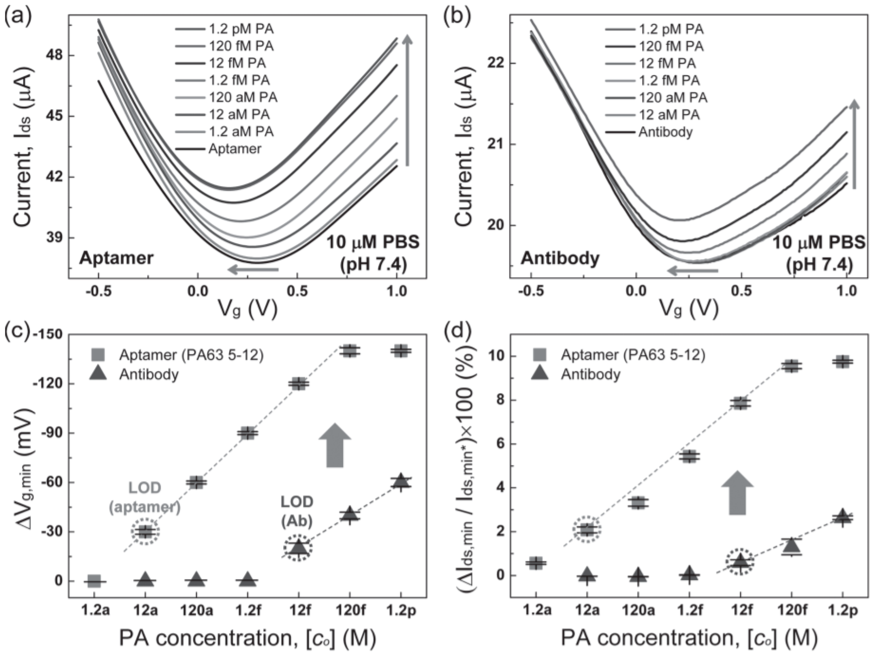
| Protective antigen (PA) | Anthrax | GO nanosheets on glass, Ti/Au contacts | Liquid gated, PA65 5–12 aptamer | 12 aM | - | - | [48] |
© 2017 by the authors. Licensee MDPI, Basel, Switzerland. This article is an open access article distributed under the terms and conditions of the Creative Commons Attribution (CC BY) license (http://creativecommons.org/licenses/by/4.0/).
Share and Cite
Forsyth, R.; Devadoss, A.; Guy, O.J. Graphene Field Effect Transistors for Biomedical Applications: Current Status and Future Prospects. Diagnostics 2017, 7, 45. https://doi.org/10.3390/diagnostics7030045
Forsyth R, Devadoss A, Guy OJ. Graphene Field Effect Transistors for Biomedical Applications: Current Status and Future Prospects. Diagnostics. 2017; 7(3):45. https://doi.org/10.3390/diagnostics7030045
Chicago/Turabian StyleForsyth, Rhiannan, Anitha Devadoss, and Owen J. Guy. 2017. "Graphene Field Effect Transistors for Biomedical Applications: Current Status and Future Prospects" Diagnostics 7, no. 3: 45. https://doi.org/10.3390/diagnostics7030045
APA StyleForsyth, R., Devadoss, A., & Guy, O. J. (2017). Graphene Field Effect Transistors for Biomedical Applications: Current Status and Future Prospects. Diagnostics, 7(3), 45. https://doi.org/10.3390/diagnostics7030045