Abstract
Surface hardening of machine parts substantially improves their performance. The best results are obtained when combined hardening consists of surface nitriding and subsequent deposition of hard coatings. The nitriding of machine parts immersed in the plasma of glow coatings have been studied, and the study results are presented. Titanium atoms for coating synthesis are obtained via titanium evaporation in a hollow molybdenum anode of the discharge. Stable evaporation of titanium occurs only when the power density of electrons heating the liquid titanium does not exceed ~500 W/cm2. To start evaporation, it is only necessary to reduce the gas pressure to 0.02 Pa. To stop evaporation, it is enough to increase the gas pressure to 0.1 Pa. Fast argon and nitrogen atoms used for cleaning the machine parts, heating them, and bombarding the growing coating are obtained using a grid composed of plane-parallel plates under high negative voltage and immersed in plasma.
1. Introduction
Ion-plasma processing of engineering products allows purposeful modification of their surface properties. Using sources of metal plasma [1] or metal vapor [2] allows the synthesis of wear-resistant coatings of carbides and nitrides of titanium, chromium, and other metals on the products. Using the method of plasma immersion ion implantation [3,4], any materials can be modified, and alloying additives can be introduced into the surface layer. Ion-plasma treatment reduces the coefficient of friction, increases the useful life of the products, and significantly increases their wear resistance and corrosion resistance. It also allows for combined treatment; for example, ion nitriding of steel products with the subsequent deposition of wear-resistant coatings [5]. In the latter case, a hardened surface layer with a thickness of 50–100 μm prevents brittle fracture of hard coatings with thickness not exceeding 5 μm. This improves the adhesion of the coating and its resistance to cracking. As a result, the product combines wear resistance with high load-bearing capacity and good fatigue strength. In plasma-immersion ion implantation, the product is immersed in a plasma containing the necessary ions, and negative high-voltage pulses are applied to it [3]. The thickness of the modified material layer is determined by the depth of ions’ penetration, which is proportional to their energy. To reach the maximum possible values of the ion energy and modification depth for a given voltage, the ions must pass through the space charge sheath between the plasma and the product surface without collisions with gas molecules. At a pressure p = 1 Pa, the mean free path of nitrogen molecules and ions is λ ≈ 6 mm, and the space charge layer width at a voltage of ~100 kV can reach d ≈ 600 mm. Therefore, the gas pressure in the working vacuum chamber should not exceed 0.01 Pa.
Plasma emitters of broad ion beam sources must be generated at the same low pressures. Here the problem is successfully solved using discharges with thermionic cathodes [6,7]. However, the useful life of thermionic cathodes is short, and they cannot be used in the environment of reactive gases, for example, oxygen. In this case, discharges without thermionic cathodes are used, for example, microwave and high-frequency discharges, as well as discharges in crossed electric and magnetic fields. Nevertheless, even when microwave sources and other sophisticated equipment are used to fill a vacuum chamber with a uniform plasma, the minimum gas pressure in the chambers of known installations exceeds 0.1 Pa [8].
The working gas pressure in the glow discharge with a cold hollow cathode always exceeded 1 Pa, until a proportional dependence of the discharge extinction pressure on the area of the cathode output aperture So was established in Reference [9]. A decrease in the output aperture of the hollow cathode with a diameter of 0.2 m and a length of 0.8 m to So ~ 0.01 S, where S is the area of the cathode inner surface, made it possible to reduce the pressure by two orders of magnitude and maintain the discharge at a pressure p ~ 0.01 Pa [10]. Based on the results achieved, sources of broad beams of fast neutral atoms [11,12,13] have been developed. They are used to etch the surface, as well as to accompany the deposition of coatings [14]. Glow discharge with a cold hollow cathode enables the filling of the chambers with homogeneous plasma and ion-plasma processing of products immersed therein [15,16]. The present research is aimed at a combined hardening of machine parts in this plasma, which determines their surface nitriding and the deposition of hard wear-resistant coatings.
2. Materials and Methods
Figure 1 shows a schematic diagram of an experimental setup with a 500 mm-diameter and 550-mm-long vacuum chamber, its volume amounting to V = 0.12 m3 and internal surface area to S = 1.5 m2. High-voltage feedthrough is installed on the upper flange of the chamber. On the feedthrough is suspended a 200 mm-diameter flat grid made of 2 mm-thick titanium sheets with 7.5 mm-diameter holes at a distance of 8 mm between their centers.
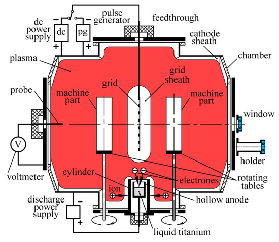
Figure 1.
Schematic diagram of the experimental setup.
On the lower flange of the chamber is mounted a water-cooled grounded hollow cylinder with an inner diameter of 40 mm and an outer diameter of 50 mm. Inside the cylinder is placed a 30-mm-deep molybdenum hollow anode with an external diameter of 34 mm and an internal diameter of 28 mm. Through the second high-voltage feedthrough, the anode is connected to a positive pole of the gas discharge power supply. Its negative pole is connected to the chamber. The upper end of the cylinder is 15 mm above the hollow anode. By installing a steel cylinder with a diameter of 28 mm and a length of 50 mm in the anode cavity, replaceable titanium disks with a thickness of 2 mm and a diameter of 5 to 15 cm can be fixed on its end. This allows for changing the effective surface area of the discharge anode from 20 to 320 cm2.
To the right and the left of the grid, two 160-mm-long and 30-mm-diameter machine parts to be hardened are fastened on tables rotating at a speed of one revolution per second (Figure 1). The rotation axes are distant from the grid at 12 cm. To learn more about the hardened surface properties, the cylindrical machine parts on the rotating tables can be replaced with 2-mm-thick 30-mm-wide and 160-mm-high plates made of high-speed steel (HSS). To measure the thickness of the nitrided layer, one of the plates can be cut for samples allowing microhardness measurements using the Micro Indentation TesterMNT produced by Anton Paar Switzerland AG (Buchs, Switzerland). Using Vickers microhardness measurements on the polished cross-section of the plate, the hardness dependence on the depth can be obtained, which allows for the evaluation of the nitrided layer’s thickness.
To measure the rate of the plate etching by fast argon atoms or the thickness of deposited coatings, five 30-mm-long and 5-mm-wide masks can be attached on the plate surfaces. After the plate etching, the masks are removed from its surface. Then, the height h of the steps between surfaces covered by the masks and open surfaces of the plate is measured using a stylus profiler DectakXT produced by Bruker Nano, Inc. (Billerica, MA, USA). The etching rate is equal to the ratio of the step height to the etching time. Similarly, the coating deposition rate is equal to the ratio of the step height to the deposition time.
The gas pressure in the chamber is measured using a VIT-3 vacuummeter with a PMI-2 ionization gauge and an MKS-vacuummeter (MKSI, Andover, MA, USA) with a transducer BARATRON. The chamber is pumped down through a grounded grid by a turbomolecular pump, providing a residual gas pressure of 0.001 Pa. Using a needle valve, the pressure inside the chamber can be adjusted from 0.001 to 5 Pa.
Using the switch, the grid can be connected to a source of negative DC bias voltage up to 5 kV or a generator of voltage pulses with an amplitude up to 25 kV, a pulse width up to 50 μs, and repetition rate of 50 Hz.
On the flange of one of the chamber doors, there is a quartz window with a diameter of 20 mm for remote measurements of the machine parts temperature with an IMPAC IP 140 pyrometer manufactured by Luma Sense Technologies GmbH (Frankfurt, Germany). To prevent the deposition of metal films on the quartz window, it can be installed on a 20-cm-long cylindrical holder with an inner diameter of 20 mm. A rod probe is introduced into the chamber through a flange on the opposite door of the chamber to measure, with voltmeters, the potential difference between the chamber and the plasma filling it, as well as between the plasma and the anode.
3. Results
When an anode disk with a diameter of 15 cm is installed in the chamber, the effective area of the anode is equal to Sa ≈ 320 cm2. Turning on the discharge power source at an argon pressure in the chamber p = 1 Pa leads to filling the chamber with a uniform plasma glow of the discharge with a voltage of U = 440 V at a current of I = 1 A. When the argon pressure decreases from p = 1 Pa to p * = 0.5 Pa, the cathode fall Uc, equal to the potential difference between the probe and the chamber, decreases from 440 V to a minimal value of 410 V and retains this value until p reaches the value po1 = 0.19 Pa and begins to increase with a further decrease in pressure (solid curve 1 in Figure 2).
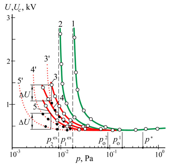
Figure 2.
Discharge voltage U (solid lines) and cathode fall Uc (dotted lines) versus argon pressure p at a current of I = 1 A and the anode surface area Sa ≈ 320 (1), 160 (2), 80 (3), 40 (4) and 20 (5) cm2. At Sa ≈ 320 and 160 cm2, Uc = U. At p = po, U starts to rise with the pressure decrease. At p = p ex, the discharge extinguishes.
With the anode disk diameter of 11 cm, the anode area is equal to Sa ≈ 160 cm2, and the cathode fall Uc begins to increase with decreasing pressure at po2 = 0.09 Pa (solid curve 2). In both previous cases, the cathode fall and the discharge voltage coincide. However, at disk diameters of 8, 6, and 5 cm, the discharge voltage U at a pressure of 0.1–1 Pa exceeds the cathode fall of potential Uc by 10–30 V, and at a pressure p ~ 0.01 Pa, the difference between them exceeds 1 kV.
With the anode disk diameter of 8 cm, the anode area Sa ≈ 80 cm2, and with decreasing pressure Uc begins to grow at p = 0.045 Pa (dotted curve 3′ in Figure 2). With a diameter of 6 cm, the anode area Sa ≈ 40 cm2 and Uc begins to grow at p = 0.022 Pa (dotted curve 4′). At a diameter of 5 cm, the anode area Sa ≈ 20 cm2 and Uc begins to grow at p = 0.011 Pa (dotted curve 5′). Comparing the dotted curves 3′, 4′, and 5′ of the cathode fall of the potential Uc with the solid curves 4, 5, and 6 of the discharge voltage U reveals a positive anode fall of potential ΔU equal to the potential difference between the anode and the plasma probe U–Uc.
With the anode disk diameter of 6 cm and argon pressure of p = 0.5 Pa, the positive anode fall of the potential is equal to ΔU ~ 25 V and a bright plasma ball is observed on the disk surface. In contrast to a gray-blue color of homogeneous plasma filling the chamber, the color of the anode plasma ball is yellow. Measurements with a pyrometer showed that the temperature of the anode disk amounts to ~250 °C. With pressure decreasing, the anode plasma ball grows in size and changes its yellow color to violet. Finally, the anode plasma disappears. Immediately, the anode fall of potential ΔU and the temperature of the anode disk T begin to increase rapidly. At p = 0.025 Pa, the anode fall of potential amounts to ΔU = 250 V, and the anode temperature measured by the pyrometer reaches T = 800 °C. At p = 0.02 Pa, the anode fall grows to ΔU = 600 V, and the edge of titanium anode disk starts to melt.
After the steel holder of the anode disks was removed from the hollow molybdenum anode, the latter was filled with fine titanium chips. When a discharge was ignited in argon with a current I = 1.5 A, a decrease in gas pressure from 0.1 to 0.02 Pa led to an increase in discharge voltage from ~0.5 to ~2.5 kV. Through the optical window on the chamber wall, rapid heating of the hollow anode and melting of titanium chips inside it were observed. Two minutes later, the window no longer allowed light through due to a metal film deposited on it.
Figure 3 shows the dependencies on the gas pressure of a positive anode fall measured as the potential difference ΔU between the anode and the probe immersed in the plasma. The values of ΔU were measured with a gradual decrease in gas pressure. However, with a rapid decrease in pressure from 0.1 to 0.02 Pa, self-excited oscillations of ΔU arise with a frequency of ~1 Hz. In this case, an increase in the ΔU and power heating liquid titanium due to the rapid decrease in the gas pressure leads to an increase in the titanium vapor pressure near the anode, resulting in a ΔU decrease. The heating power diminishes, which leads to a decrease in the temperature of the liquid titanium and the pressure of its vapor. This causes an increase in ΔU; the titanium pressure rises again, and so on.
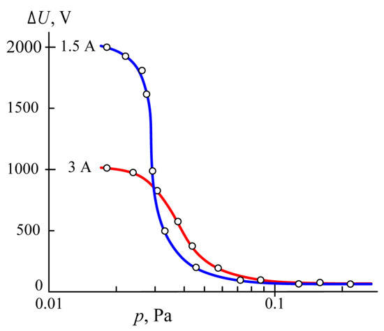
Figure 3.
Dependences on the argon pressure p of the potential difference ΔU between the anode and the probe immersed in the plasma at the discharge currents I = 1.5 A and 3 A.
At a discharge current of I = 1.5 A, ΔU grows from ~30 V at p = 0.1 Pa to ~200 V at p = 0.045 Pa and to ~1000 V at p = 0.03 Pa. Furthermore, the anode fall ΔU sharply rises to ~1800 V at p = 0.025 Pa. Then, its growth slows down, and until the discharge expires at p = 0.015 Pa, it reaches ΔU ~2000 V. The maximal power heating the liquid titanium in the hollow anode amounts to ~2000 × 1.5 = 3000 W. At a discharge current of I = 3 A, the maximal value of the positive anode fall is equal to ΔU ~ 1000 V. Hence, the maximal power heating the liquid titanium also amounts to ~1000 × 3 = 3000 W. On the liquid surface with an area of ~6 cm2, this corresponds to an average power density of ~500 W/cm2. Therefore, the curves in Figure 3 show that stable evaporation of titanium in the hollow anode occurs only when the heating power density does not exceed ~500 W/cm2. To start evaporation, it is only necessary to reduce the gas pressure to 0.02 Pa. To stop evaporation, it is enough to increase the gas pressure to 0.1 Pa.
At a discharge current of I = 3 A, application to the grid (see Figure 1) of negative DC bias voltage U ~ 5 kV leads to the appearance of two broad beams propagating in opposite directions. Due to kinetic ion-electron emission [17,18,19] from the grid surface, beams of electrons with an energy of e(U + Uc) are produced.
Ions accelerated in the sheath of the positive space charge surrounding the grid pass through its holes and are decelerated on the other side of the grid. Then they are accelerated back to the grid, pass through its holes again, and so on (Figure 4). The average path of ions repeatedly flying through the holes of the grid is equal to
where η = 0.8 is the grid transparency, and the sheath width d according to the Child-Langmuir law [20] is equal to
where εo is the electric constant equal to 0.885 × 10⁻¹¹ F/m, e is the electron charge, M is the ion mass, and j is the ion current density. When the ion mass M = AMA is measured in atomic mass units A = 1.66 × 10⁻²⁷ kg, the sheath width is equal to
L = 2d/(1 − η),
d = (2/3)εo1/2(2e/M)1/4(U + Uc)3/4/j1/2,
d = 2.34 × 10⁻⁴(MA)−1/4(U + Uc)3/4/j1/2
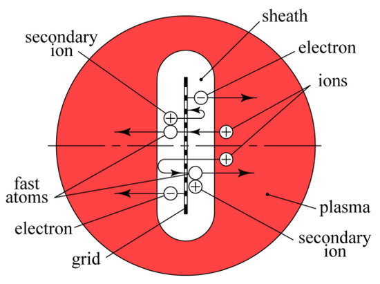
Figure 4.
Schematic of fast atoms formation due to charge exchange collisions of ions.
At a discharge current of Id = 3 A, the ion current in the grid circuit is equal to Ig ≈ 0.3 A, and the mean ion current density amounts to j = Ig/Sg ≈ 4.8 A/m2, where the grid surface area is equal to Sg = 0.0628 m2. For j = 4.8 A/m2, U ≈ 5000 V, Uc ≈ 500 V and MA = 40, the sheath width between the plasma and the grid amounts to d ≈ 2.71 cm. For the grid transparency of η = 0.8, the length of the ion path in the sheath before absorption by the grid is equal to L = 2d/(1 − η) ≈ 27 cm.
The charge exchange cross-section for argon ions with an energy of 5500 eV is equal to σ = 1.7 × 10⁻¹⁹ m2 [21,22]. At a pressure of p = 0.02 Pa, the density of gas atoms is equal to no = 0.5 × 10¹⁹ m−3 [23], and the charge exchange length λc = 1/noσc ≈ 1.2 m by more than four times exceeds the ion path to the grid surface L = 0.27 m. Therefore, no fast neutral atoms appear at p = 0.02 Pa, and all the ions reciprocating in the sheath bombard the grid with the energy of 5500 eV. At this energy of argon, the ion coefficient of kinetic ion-electron emission for titanium is equal to γ = 1.8 [16]. This means that at the ion current in the grid circuit of Ig ≈ 0.3 A, it emits two beams of 5500-eV electrons, with their total current amounting to Ie ≈ γIg ≈ 0.54 A.
These fast electrons can effectively heat machine parts before nitriding and coating deposition. The power density they transport amounts to w = 4.76 × 10⁴ W/m2. When the electrons heat one side of a flat steel plate, the luminosity of its surface is two times lower and amounts to R* = 2.38 × 10⁴ W/m2. According to the Stefan-Boltzmann law, luminosity R* of the plate is equal to
where σS-B = 5.7 × 10⁻⁸ W/(m2⋅K4) is the Stefan-Boltzmann constant and ω ~ 0.25 is the emissivity factor for steel. It is equal to the above luminosity R* = 2.38 × 10⁴ W/m2 at the plate temperature of T = 865 °C.
R* = ωϭS-BT4,
When the argon pressure grows by five times to p = 0.1 Pa, the charge exchange length diminishes to λc = 0.24 m < L = 0.27 m. In these conditions, most of the ions accelerated from the plasma turn into fast neutral atoms before being absorbed by the grid. The energy of a fast atom corresponds to the potential difference between the point of its charge exchange collision and the grid. It reaches the maximal value ~e (U + Uc) when the collision occurs in the grid hole and diminishes to zero when the collision occurs near the sheath border (Figure 4).
When argon pressure grows to p = 1 Pa, the charge exchange length diminishes to λc = 2.4 mm and is about 11 times less than the sheath width d = 27 mm. In this case, one ion with ~0.5-keV energy and ten fast neutral atoms of about the same energy cross the grid instead of one ion with 5.5-keV energy. The fast atoms do not give rise to the electron emission, because kinetic ion-electron emission takes place only when the energy of the bombarding particles exceeds ~0.5 keV [24].
At the coefficient of potential ion-electron emission γ ~ 0.05, the current of electrons emitted by the grid is 20 times lower than the ion current Ig in its circuit. In this case, the equivalent beam current Ib of the produced fast neutral particles with a mean energy e(U + Uc)λc/d ≈ 0.1e(U + Uc) grows up to Ib ≈ ηIg d/λc = 10ηIg, where η = 0.8 is the geometrical transparency of the grid. The equivalent current of fast particles that bombard and sputter the grid is equal to (1 − η)Igd/λc, and within the above range of parameters, we may suggest the sputtering coefficient to be proportional to their energy e(U + Uc)λc/d. Hence, at a constant current in the grid circuit, the sputtering rate reduces about 1/(1 − η) = 5 times, with pressure increasing from 0.05 up to 1 Pa.
It should be emphasized that at a constant discharge current Id and grid voltage U, the heating power density is almost independent of the pressure. The only thing is that at p = 0.02 Pa, it is transported solely by electrons, at p ~ 0.1 Pa by electrons and fast atoms with energies of a few keV, and at p ~ 1 Pa mainly by fast atoms with energies that are lower by an order of magnitude of a few hundred eV. Measurements showed that at argon pressure p = 0.1 Pa, Id = 3 A, and U = 5 kV, two 160-mm-long and 30-mm-diameter machine parts (Figure 1) rotating at a speed of one revolution per second have been heated to 500 °C for 12 min. To prevent the optical window from the deposition of metal films, it was installed on a 20-cm-long cylindrical holder with an inner diameter of 20 mm. After the argon pressure was decreased to 0.02 Pa, evaporation of titanium from the hollow anode started, and the machine parts were coated with titanium.
When nitrogen was supplied to the chamber instead of argon, heating of the cylinders to 500 °C at p ~ 0.1 Pa was followed by the coating deposition at p = 0.02 Pa. After a 2-h-long etching, the polished plate at an argon pressure of p = 1 Pa, Id = 3 A, and U = 5 kV, the masks were removed from its surface. The height h of the between steps covered by the masks and open surfaces of the plate was measured (Figure 5). For the center of the plate, it amounts to h = 1.2 μm, thus indicating that the sputtering rate is equal to v = 0.6 μm/h.
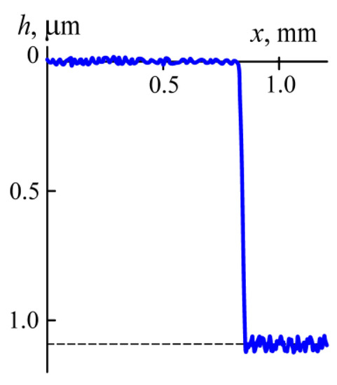
Figure 5.
Profilogram of a plate surface covered with a mask and bombarded with fast argon atoms.
Curve 1 in Figure 6 presents the dependence of the plate etching rate v on distance x from the table surface at the argon pressure of p = 0.2 Pa. It demonstrates a quite homogeneous etching distribution. The same measurements were carried out at the argon pressure of p = 1 Pa (curve 2).
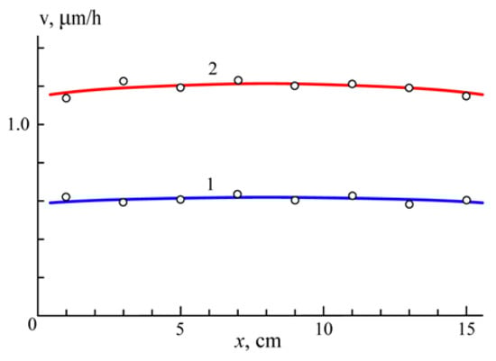
Figure 6.
The etching rate v versus the distance x from the table at p = 0.1 (1) and 1 (2) Pa.
Masks on the plates were also used for measurement of the coating thickness. After cleaning a rotating plate at the discharge current Id = 1.5 A and argon pressure p = 1 Pa for 10 min, its temperature increased to 450 °C. Then, the pressure was reduced to p = 0.02 Pa, the anode fall of potential increased to ~2000 V, and the deposition of a titanium coating on the plate began. Since at p = 0.02 Pa, the fast atoms are not formed, the coating adhesion was very poor. Hence, at p = 0.02 Pa, when the rate of titanium evaporation is maximal, it is impossible to bombard the growing coating with fast atoms, as in References [25,26,27].
To solve this problem, the round 2-mm-thick grid was replaced with a 25-mm-thick rectangular grid composed of 33 plane-parallel 25-mm-wide, 160-mm-long, and 0.5-mm-thick titanium plates distanced from each other at 4.5 mm (Figure 7). Ions accelerated in the sheath between the plasma and the grid are reflected from the lateral surfaces of the plates and are absorbed only by their ends. Therefore, the grid transparency is equal to η = 4.5/5 = 0.9, and the average path of accelerated ions through the sheath L is also determined by Equation (1). At the same ion current density j = 4.8 A/m2 and grid voltage (U + Uc) = 5500 V, the sheath width is equal to d = 27 mm, and the path length amounts to L = 0.27 m. It is necessary to add the length of 2/(1 − η) = 20 flights of the ions between 25-mm-wide plates, which is equal to Lo = 0.25 × 20 = 0.5 m. Altogether, the pass of accelerated ions to the grid surface amounts to L + Lo = 0.77 m, which is less than their charge exchange length λc ≈ 1.2 m at argon pressure p = 0.02 Pa. Hence, the probability of the appearance of the fast atom due to collisions of accelerated ions with gas molecules is negligible. Therefore, in the case of a grid composed of plane-parallel plates, fast atoms are formed at p = 0.02 Pa only due to the recombination of ions flying between the plates and electrons emitted by the plates upon contacts of ions with them (potential ion-electron emission).
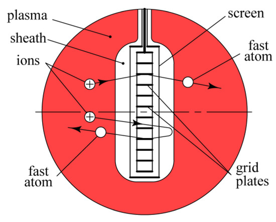
Figure 7.
A schematic of fast atom formation due to the recombination of ions and electrons pulled out by the ions from the grid plates.
Ions touch the plates due to angular scattering in an inhomogeneous electric field in the sheath near the ends of the plates. If contact with the plates did not take place during the first flight through the grid, the ion returns and flies through the grid again. After several flights, the ion finally turns into a fast neutral atom with an energy of e(U + Uc) ≈ 5500 eV.
To eliminate inhomogeneity of the electric field on the grid periphery and an intensive sputtering of outer surfaces of the upper and lower plates by ions accelerated from the plasma, the 25-mm-thick grid is surrounded with a grounded screen made of 30-mm-wide and 2-mm-thick titanium strip.
Nitrogen was introduced into the chamber and, at a gas pressure of p = 0.2 Pa, a discharge with a current of Id = 3 A, and a voltage of ~500 V was ignited. After applying voltage U = 5000 V to the grid, the temperature of the rotating plates rapidly increased for 10 min to 450 °C. At p = 0.2 Pa, the power heating the hollow anode was negligible, and visual observations through the window showed that after heating the plates with electrons and cleaning them with fast atoms, the color of their surfaces did not change.
The above temperature of 450 °C was kept for 60 min, utilizing the discharge current regulation in the range of Id = 2–2.5 A. After that, plates were taken out of the chamber, and one of them was cut for samples. The measurements showed that the microhardness of the surface increased by 1.5 times from 850HV0.05 to 1300HV0.05. Using Vickers microhardness measurements on the polished cross-section of the plate under a load of 50 g, the hardness and depth of the surface layer were evaluated. Figure 8 shows that the depth of the nitrided surface layer amounts to ~100 μm.
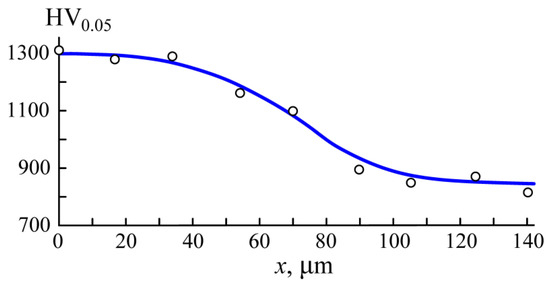
Figure 8.
Dependence of the microhardness HV0.05 on the distance x from the sample surface.
Another pair of polished HSS plates have been exposed to the same 2-h-long procedure of nitriding. On the surface of one of the plates, eight masks were previously fixed. After nitriding, the grid was disconnected from the DC bias voltage power supply and connected to the pulse generator (Figure 1). At the nitrogen pressure of p = 0.2 Pa, the pulse generator was switched on and the rotating plates were exposed to pulsed beams of fast nitrogen atoms with the energy of 30 keV following each other with the repetition rate of 50 Hz, the pulse width being equal to 50 μs.
After the fast atoms started to mix the atoms in the surface layers of the plates, the gas pressure was diminished to p = 0.02 Pa. As a result, titanium evaporation in the hollow anode and synthesis of titanium nitride coating on the rotating plates started. An hour later, the titanium nitride coatings were synthesized on the plates. Figure 9 presents an X-ray diffraction pattern of the coating obtained using the PANalytical Empyrean Series 2 X-ray diffractometer with monochromatic CuKα radiation in asymmetric geometry. The radius of the high-resolution goniometer was equal to 240 mm. Measurements were carried out in the range from 10 to 100 degrees with a resolution of 0.0001 degrees.
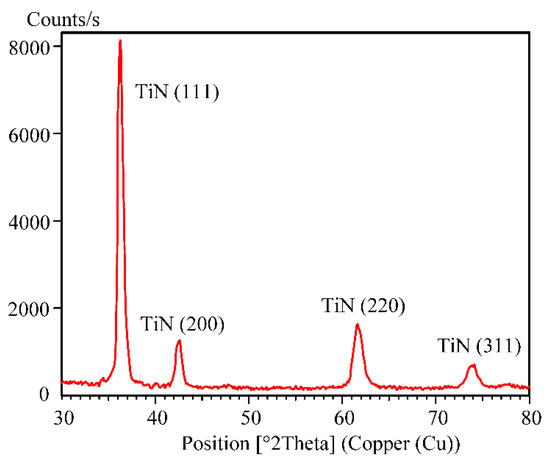
Figure 9.
X-ray diffraction pattern of the coating synthesized in the center of the plate.
The XRD indicates that the synthesized coating contains only one phase of TiN, which is in good agreement with its golden color. Using the Micro Indentation TesterMNT produced by Anton Paar Switzerland AG (Buchs, Switzerland), the microhardness of the coating deposited on the nitrided layer has been measured. It amounts to a standard for the TiN value of 2300 HV0.05.
The coating thickness was defined after removing the masks from the plate surface and measuring the height of the steps between covered with masks and the open surface of the plate. The thickness monotonically decreases from 3.2 μm near the lower end of the plate to 2.8 μm near its upper end. The X-ray diffraction pattern of 3.2-μm-thick coating does not differ from that of 2.8-μm-thick coating. This means that the coating composition does not change with the distance from the source of titanium vapor. Presented in Figure 10, the dependence of the normal force and acoustic emission on the scratch length obtained using a Nanovea M1 Hardness and Scratch Tester produced by Nanovea Mechanical Testing (Nanovea INC, Irvine, CA, USA) reveals an acceptable adhesion of the TiN coating to the plate. For the scratch test, a conical diamond indenter with a tip radius of 100 μm was used. The applied load on the indenter was up to 30 N. The scratch length was equal to 5 mm.
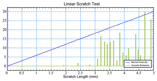
Figure 10.
The dependence on the scratch length of the normal force and acoustic emission.
The adhesion is characterized by the first critical load, at which acoustic emission occurs of about 19 N. It is ensured due to the mixing by high-energy gas atoms of the plate material and coating atoms from the very beginning of the coating deposition process, and hence, at the interface formation stage.
4. Discussion
The above results show that the combined processing of machine parts previously carried out mainly in the vacuum arc discharge can be successfully realized in the glow discharge. Principles of the electrostatic confinement of fast electrons in glow discharge provide for a wide spectrum of novelties in the ion-plasma processing of machine parts and other products. In contrast to vacuum arc and magnetron discharges, it is possible to fill any process vacuum chamber with quite homogeneous plasma at gas pressures ranging from ~0.001 to ~10 Pa. It allows for generating broad beams of fast neutral atoms with a uniform distribution of the flow density and quite homogeneous etching of machine parts (Figure 6).
The etching rate grows two-fold when the gas pressure rises from 0.2 to 1 Pa. Experimental results allow the assumption that this is due to an increase in the number of charge exchange collisions of ions and gas molecules in the grid sheath. At a constant ion current in the grid circuit, it leads to an increase in the number of fast atoms and a decrease in their mean energy. The energy of ions impinging on the grid diminishes. This leads to a substantial decrease in the current of secondary electrons. Hence, the gas pressure should exceed 1 Pa when effective etching is needed. It should be mentioned that the experimental setup presented in Figure 1 could be also used for an effective etching by fast neutral atoms of any dielectric products.
At a low pressure of p < 0.1 Pa, application to a conductive product of high-voltage pulses allows the implantation into its surface layer of any alloying additions and modification of its structure [28,29,30]. Because of the inhomogeneity of the ion current density on the surface of a complex-shaped product, the implantation dose distribution should be also inhomogeneous. When high-voltage pulses are applied to a grid composed of plane-parallel plates (Figure 7), pulsed beams of fast neutral atoms with a uniform distribution of flow density are generated. Rotation of the machine parts under processing by homogeneous beams ensures the homogeneity of the implantation dose distribution. It should be also mentioned that the experimental setup presented in Figure 1 could be also used for the implantation of fast neutral atoms into any dielectric products.
The main novelty of the setup is the evaporation of liquid metal in a hollow anode of the discharge. In contrast to vacuum arc evaporation [31,32,33,34,35,36,37,38,39,40], the flow of metal vapor from the hollow anode does not contain metal droplets. In contrast to magnetron sputtering [41,42,43,44,45,46,47,48,49,50], the coating deposition rate does not diminish at all when reactive gases are added to argon or replace it. For the first time, the melting and evaporation of a titanium anode were observed in Reference [51]. In our case, the discharge characteristics for various areas of the disc anodes (Figure 2) proved that a positive anode fall in potential occurs when the anode area Sa is less than a critical value
where e is the Naperian base, m and M are the electron mass and the ion mass, and S is the chamber surface area. For discharge in argon and S = 1.5 m2, the critical anode area amounts to S* = 0.008 m2. Only at the disc anode area of Sa ≈ 80 cm2 were the positive anode fall of potential and the anode plasma ball observed. At the lower anode area of Sa ≈ 40 cm2, the melting of the anode disc already started with the decrease in pressure.
S* = (π/e) 1/2(2m/M)1/2S ≈ (2m/M)1/2S,
In the case of the hollow molybdenum anode with the bottom area of 6 cm2, a decrease in pressure from 0.1 to 0.02 Pa initiated self-excited oscillations of anode fall of potential ΔU with a frequency of ~1 Hz. The oscillations are caused by an increase in pressure of metal vapor due to the high heating power of ΔU × Id, which in turn leads to a decrease in ΔU and pressure. However, the use of a needle valve for the gas supply into the chamber ensures a slow variation of the gas pressure without oscillations. It turned out that stable evaporation of titanium in the hollow anode occurs only when the heating power density does not exceed ~500 W/cm2. To start evaporation, it is only necessary to slowly reduce the gas pressure to 0.02 Pa. To stop evaporation, it is enough to increase the gas pressure to 0.1 Pa.
5. Conclusions
- The plasma of glow discharge with electrostatic confinement of electrons provides for the generation of a flow of titanium vapor and broad beams of fast atoms to assist the coating deposition.
- Heating the rotating machine parts using fast nitrogen atoms allows for nitriding without damages to the surface from cathode arc spots, which often occur while heating via ions accelerated from the plasma by a negative bias voltage.
- Quite good adhesion of TiN coatings synthesized on the machine parts is ensured by mixing atoms of the machine parts’ material and the coating material with high-energy gas atoms from the very outset of the deposition at the interface formation stage.
- It is reasonable to use the above experimental results for the further processing of dielectric products.
Author Contributions
Conceptualization, A.M. and S.G.; formal analysis, S.G.; funding acquisition, S.G.; investigation, A.M., Y.M. and E.M.; methodology, M.V., and Y.M.; project administration, M.V.; resources, S.G. and M.V.; software, E.M.; validation, S.G., M.V. and A.M.; supervision, S.G.; visualization, Y.M.; writing—original draft preparation, M.V.; writing—review and editing, E.M. All authors have read and agreed to the published version of the manuscript.
Funding
This work is funded by the state assignment of the Ministry of Science and Higher Education of the Russian Federation, project No. 0707-2020-0025.
Acknowledgments
The research was carried out at the Department of High-Efficiency Processing Technologies of MSTU STANKIN.
Conflicts of Interest
The authors declare no conflict of interest.
References
- Anders, A. Cathodic Arcs: From Fractal Spots to Energetic Condensation; Springer: New York, NY, USA, 2008. [Google Scholar]
- Warner, B.E.; Persson, K.B.; Collins, G.J. Metal-vapor production by sputtering in a hollow-cathode discharge: Theory and experiment. J. Appl. Phys. 1979, 50, 5694–5703. [Google Scholar] [CrossRef]
- Anders, A. (Ed.) Handbook of Plasma Immersion Ion Implantation and Deposition; John Wiley & Sons: New York, NY, USA, 2000. [Google Scholar]
- Grigoriev, S.N.; Melnik, Y.A.; Metel, A.S.; Panin, V.V. Broad beam source of fast atoms produced as a result of charge exchange collisions of ions accelerated between two plasmas. Instrum. Exp. Tech. 2009, 52, 602–608. [Google Scholar] [CrossRef]
- Avelar-Batista, J.C.; Spain, E.; Housden, J.; Matthews, A.; Fuentes, G.G. Plasma nitriding of Ti6Al4V alloy and A1S1M2 steel substrates using DC glow discharge under a triode configuration. Surf. Coat. Technol. 2005, 200, 1954–1961. [Google Scholar] [CrossRef]
- Hayes, A.V.; Kanarov, V.; Vidinsky, B. Fifty centimeter ion beam source. Rev. Sci. Instrum. 1996, 67, 1638–1641. [Google Scholar] [CrossRef]
- Koval, N.N.; Ryabchikov, A.I.; Sivin, D.O.; Lopatin, I.V.; Krysina, O.V.; Akhmadeev, Y.H.; Ignatov, D.Y. Low-energy high-current plasma immersion implantation of nitrogen ions in plasma of non-self-sustained arc discharge with thermionic and hollow cathodes. Surf. Coat. Technol. 2018, 340, 152–158. [Google Scholar] [CrossRef]
- Vempaire, D.; Pelletier, J.; Lacoste, A.; Bechu, S.; Sirou, J.; Miraglia, S.; Fruchart, D. Plasma-based ion implantation: A valuable technology for the elaboration of innovative materials and nanostructured thin films. Plasma Phys. Control. Fusion. 2005, 47, 153–166. [Google Scholar] [CrossRef]
- Metel, A.S. Effect of ionization in the cathode layer on the characteristics of a Penning discharge. I. Hollow cathode discharge. Zh. Techn. Fiz. 1985, 30, 1133–1136. [Google Scholar]
- Oks, E.M.; Vizir, A.V.; Yushkov, G.Y. Low-pressure hollow-cathode glow discharge plasma for broad beam gaseous ion source. Rev. Sci. Instrum. 1998, 69, 853–855. [Google Scholar] [CrossRef]
- Grigoriev, S.; Melnik, Y.; Metel, A. Broad fast neutral molecule beam sources for industrial-scale beam-assisted deposition. Surf. Coat. Technol. 2002, 156, 44–49. [Google Scholar] [CrossRef]
- Vizir, A.V.; Yushkov, G.Y.; Oks, E.M. Further development of a gaseous ion source based on low-pressure hollow cathode glow. Rev. Sci. Instrum. 2000, 71, 728–730. [Google Scholar] [CrossRef]
- Metel, A.S.; Grigoriev, S.N.; Melnik, Y.A.; Bolbukov, V.P. Broad beam sources of fast molecules with segmented cold cathodes and emissive grids. Instrum. Exp. Tech. 2012, 55, 122–130. [Google Scholar] [CrossRef]
- Grigoriev, S.; Metel, A. Plasma- and Beam-Assisted Deposition Methods. In NATO Science Series, Series II: Mathematics, Physics and Chemistry Book Series NAII; Voevodin, A.A., Shtansky, D.V., Levashov, E.A., Moore, J.J., Eds.; Springer: Berlin, Germany, 2004; pp. 147–154. ISBN 9781402022227. [Google Scholar] [CrossRef]
- Korolev, Y.D.; Koval, N.N. Low-pressure discharges with hollow cathode and hollow anode and their applications. J. Phys. D: Appl. Phys. 2018, 51, 323001. [Google Scholar] [CrossRef]
- Metel, A.S.; Grigoriev, S.N.; Melnik, Y.A.; Prudnikov, V.V. Glow discharge with electrostatic confinement of electrons in a chamber bombarded by fast electrons. Plasma Phys. Rep. 2011, 37, 628–637. [Google Scholar] [CrossRef]
- Cousinie, P.; Colombie, N.; Fert, C.; Simon, R. Variation du coefficient d’emission electronique secondaire de quelques metaux avec l’energie des ions incidents. C. R. Acad. Sci. 1959, 243, 387–389. [Google Scholar]
- Shamim, M.M.; Scheuer, J.T.; Fetherston, R.P.; Conrad, J.R. Measurement of electron emission due to energetic ion bombardment in plasma source ion implantation. J. Appl. Phys. 1991, 70, 4756–4759. [Google Scholar] [CrossRef]
- Baglin, V.; Bojko, J.; Gröbner, O.; Henrist, B.; Hilleret, N.; Scheuerlein, C.; Taborelli, M. The secondary electron yield of technical materials and its variation with surface treatments. In Proceedings of the 7th European Particle Accelerator Conference, Vienna, Austria, 26–30 June 2000; pp. 217–221. [Google Scholar]
- Langmuir, I. The interaction of electron and positive ion space charges in cathode sheaths. Phys. Rev. 1929, 33, 954–989. [Google Scholar] [CrossRef]
- Phelps, A.V. Cross sections and swarm coefficients for nitrogen ions and neutrals in N2 and argon ions and neutrals in Ar for energies from 0.1 eV to 10 keV. J. Phys. Chem. Ref. Data. 1991, 20, 557–573. [Google Scholar] [CrossRef]
- Phelps, A.V.; Greene, C.H.; Burke, J.P. Collision cross sections for argon atoms with argon atoms for energies from 0.01 eV to 10 keV. J. Phys. B At Mol. Opt. Phys. 2000, 33, 2965–2981. [Google Scholar] [CrossRef]
- McDaniel, E.W. Collision Phenomena in Ionized Gases; Willey: New York, NY, USA, 1964. [Google Scholar]
- Kaminsky, M. Atomic and Ionic Impact Phenomena on Metal Surfaces; Springer-Verlag: Berlin, Germany, 1965. [Google Scholar]
- Metel, A.; Bolbukov, V.; Volosova, M.; Grigoriev, S.; Melnik, Y. Equipment for deposition of thin metallic films bombarded by fast argon atoms. Instrum. Exp. Tech. 2014, 57, 345–351. [Google Scholar] [CrossRef]
- Metel, A.S.; Grigoriev, S.N.; Melnik, Y.A.; Bolbukov, V.P. Characteristics of a fast neutral atom source with electrons injected into the source through its emissive grid from the vacuum chamber. Instrum. Exp. Tech. 2012, 55, 288–293. [Google Scholar] [CrossRef]
- Metel, A.; Bolbukov, V.; Volosova, M.; Grigoriev, S.; Melnik, Y. Source of metal atoms and fast gas molecules for coating deposition on complex shaped dielectric products. Surf. Coat. Technol. 2013, 225, 34–39. [Google Scholar] [CrossRef]
- Ruset, C.; Grigore, E. The influence of ion implantation on the properties of titanium nitride layer deposited by magnetron sputtering. Surf. Coat. Technol. 2002, 156, 159–161. [Google Scholar] [CrossRef]
- Ruset, C.; Grigore, E.; Collins, G.A.; Short, K.T.; Rossi, F.; Gibson, N.; Dong, H.; Bell, T. Characteristics of the Ti2N layer produced by an ion-assisted deposition method. Surf. Coat. Technol. 2003, 174-175, 698–703. [Google Scholar] [CrossRef]
- Grigore, E.; Ruset, C.; Short, K.T.; Hoeft, D.; Dong, H.; Li, X.Y.; Bell, T. In situ investigation of the internal stress within the nc-Ti2N/nc-TiN nanocomposite coatings produced by a combined magnetron sputtering and ion implantation method. Surf. Coat. Technol. 2005, 200, 744–747. [Google Scholar] [CrossRef]
- Shashurin, A.; Beilis, I.I.; Boxman, R.L. Experimental study of plasma parameters in a vacuum arc with a hot refractory anode. Plasma Sources Sci. Technol. 2009, 18, 045004. [Google Scholar] [CrossRef]
- Aksenov, I.I.; Aksyonov, D.S. Vacuum arc plasma source with rectilinear filter for deposition of functional coatings. Funct. Mater. 2008, 15, 442–447. [Google Scholar]
- Anders, A.; Pasaja, N.; Sansongsiri, S. Filtered cathodic arc deposition with ion-species-selective bias. Rev. Sci. Instrum. 2007, 78, 063901. [Google Scholar] [CrossRef]
- Kleiman, A.; Marquez, A.; Boxman, R.L. Performance of a magnetic island macroparticle filter in a titanium vacuum arc. Plasma Sources Sci. Technol. 2008, 17, 015008. [Google Scholar] [CrossRef]
- Beilis, I.; Shashurin, A.; Boxman, R.L. Anode plasma plume development in a vacuum arc with a “black-body” anode-cathode assembly. IEEE Trans. Plasma Sci. 2008, 36, 1030–1031. [Google Scholar] [CrossRef]
- Sangines, R.; Bilek, M.M.M.; McKenzie, D.R. Optimizing filter efficiency in pulsed cathodic vacuum arcs operating at high currents. Plasma Sources Sci. Technol. 2009, 18, 045007. [Google Scholar] [CrossRef]
- Sato, A.; Iwao, T.; Yumoto, M. Relation between surface roughness and number of cathode spots of a low-pressure arc. Plasma Sources Sci. Technol. 2008, 17, 045007. [Google Scholar] [CrossRef]
- Rysanek, F.; Burton, R.L. Charging of microparticles in a pulsed vacuum arc discharge. IEEE Trans. Plasma Sci. 2008, 36, 2147–2162. [Google Scholar] [CrossRef]
- Paperny, V.L.; Chernich, A.A.; Astrakchantsev, N.V.; Lebedev, N.V. Ion acceleration at different stages of a pulsed vacuum arc. J. Phys. D Appl. Phys. 2009, 42, 155201. [Google Scholar] [CrossRef]
- Ehiasarian, A.P.; Anders, A.; Petrov, I. Combined filtered cathodic arc etching pretreatment–magnetron sputter deposition of highly adherent CrN films. J. Vac. Sci. Technol. A. 2007, 25, 543–550. [Google Scholar] [CrossRef]
- Horwat, D.; Anders, A. Spatial distribution of average charge state and deposition rate in high power impulse magnetron sputtering of copper. J. Phys. D Appl. Phys. 2008, 41, 135210. [Google Scholar] [CrossRef]
- Oks, E.; Anders, A. Evolution of the plasma composition of a high power impulse magnetron sputtering system studied with a time-of-flight spectrometer. J. Appl. Phys. 2009, 105, 093304. [Google Scholar] [CrossRef]
- Anders, A. Discharge physics of high power impulse magnetron sputtering. Surf. Coat. Technol. 2011, 205, S1–S9. [Google Scholar] [CrossRef]
- Anders, A.; Capek, J.; Hala, M.; Martinu, L. The ‘recycling trap’: A generalized explanation of discharge runaway in high-power impulse magnetron sputtering. J. Phys. D Appl. Phys. 2012, 45, 012003. [Google Scholar] [CrossRef]
- Greczynski, G.; Hultman, L. Time and energy resolved ion mass spectroscopy studies of the ion flux during high power pulsed magnetron sputtering of Cr in Ar and Ar/N2 atmospheres. Vacuum. 2010, 84, 1159–1170. [Google Scholar] [CrossRef]
- Anders, A. A plasma lens for magnetron sputtering. IEEE Trans. Plasma Sci. 2011, 39, 2528–2529. [Google Scholar] [CrossRef]
- Sarakinos, K.; Alami, J.; Konstantinidis, S. High power pulsed magnetron sputtering: A review on scientific and engineering state of the art. Surf. Coat. Technol. 2010, 204, 1661–1684. [Google Scholar] [CrossRef]
- Hala, M.; Viau, N.; Zabeida, O.; Klemberg-Sapieha, J.E.; Martinu, L. Dynamics of reactive high-power impulse magnetron sputtering discharge studied by time- and space-resolved optical emission spectroscopy and fast imaging. J. Appl. Phys. 2010, 107, 043305. [Google Scholar] [CrossRef]
- Musil, J.; Baroch, P. High-rate pulsed reactive magnetron sputtering of oxide nanocomposite coatings. Vacuum 2013, 87, 96–102. [Google Scholar] [CrossRef]
- Musil, J. Hard nanocomposite coatings: Thermal stability, oxidation resistance and toughness. Surf. Coat. Technol. 2012, 207, 50–65. [Google Scholar] [CrossRef]
- Metel, A.S.; Grigoriev, S.N.; Melnik, Y.A.; Panin, V.V. Filling the vacuum chamber of a technological system with homogeneous plasma using a stationary glow discharge. Plasma Phys. Rep. 2009, 35, 1058–1067. [Google Scholar] [CrossRef]
© 2020 by the authors. Licensee MDPI, Basel, Switzerland. This article is an open access article distributed under the terms and conditions of the Creative Commons Attribution (CC BY) license (http://creativecommons.org/licenses/by/4.0/).