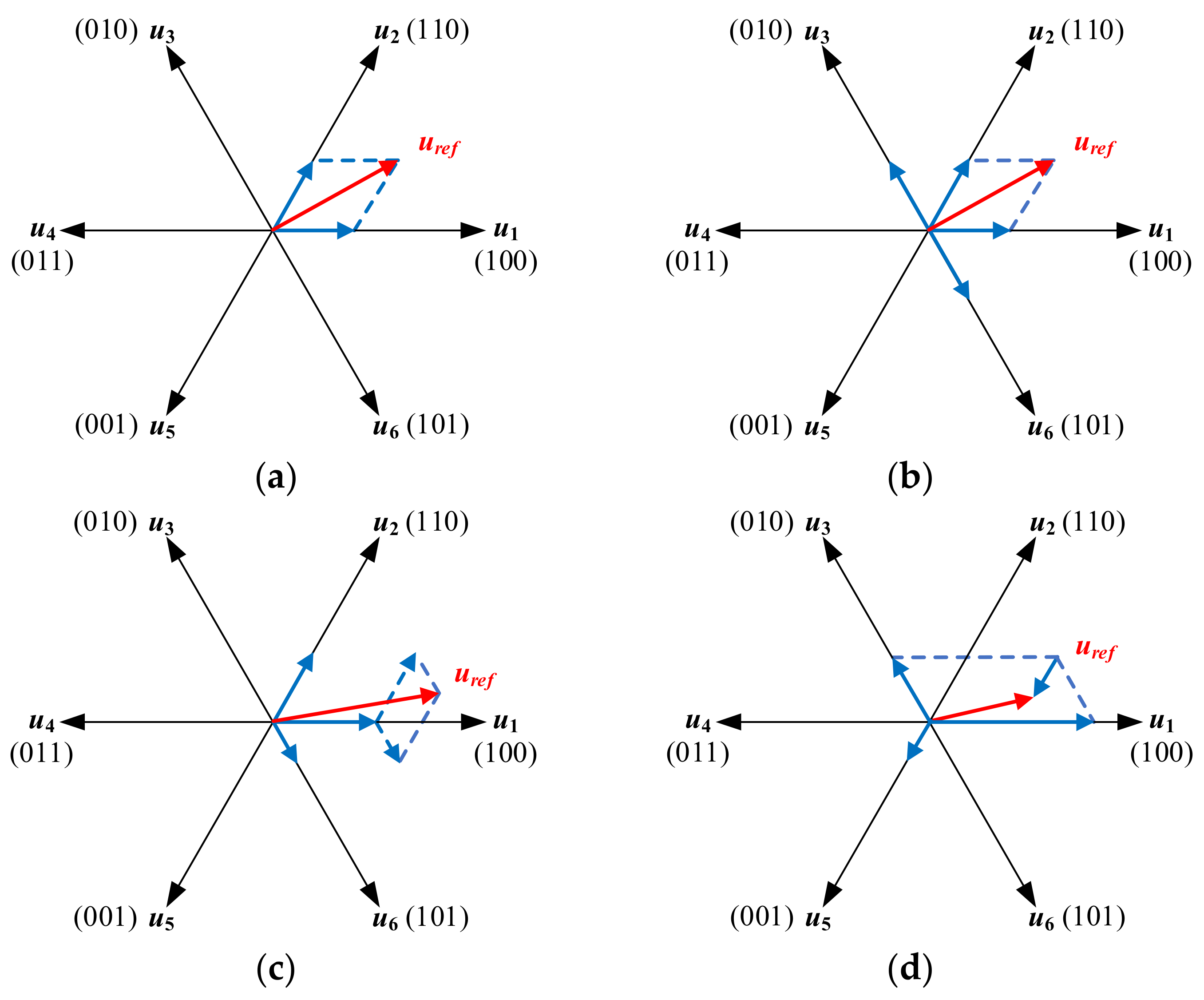
Figure 1.
Modulation strategies summary. (a) SVPWM. (b) AZSPWM. (c) NSPWM. (d) RSPWM.
Figure 1.
Modulation strategies summary. (a) SVPWM. (b) AZSPWM. (c) NSPWM. (d) RSPWM.
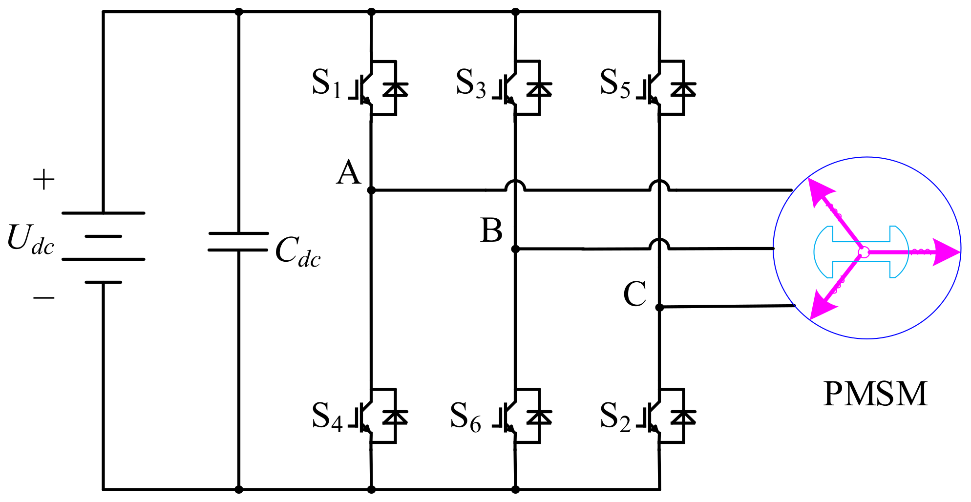
Figure 2.
The topology of VSI fed PMSM drive system.
Figure 2.
The topology of VSI fed PMSM drive system.
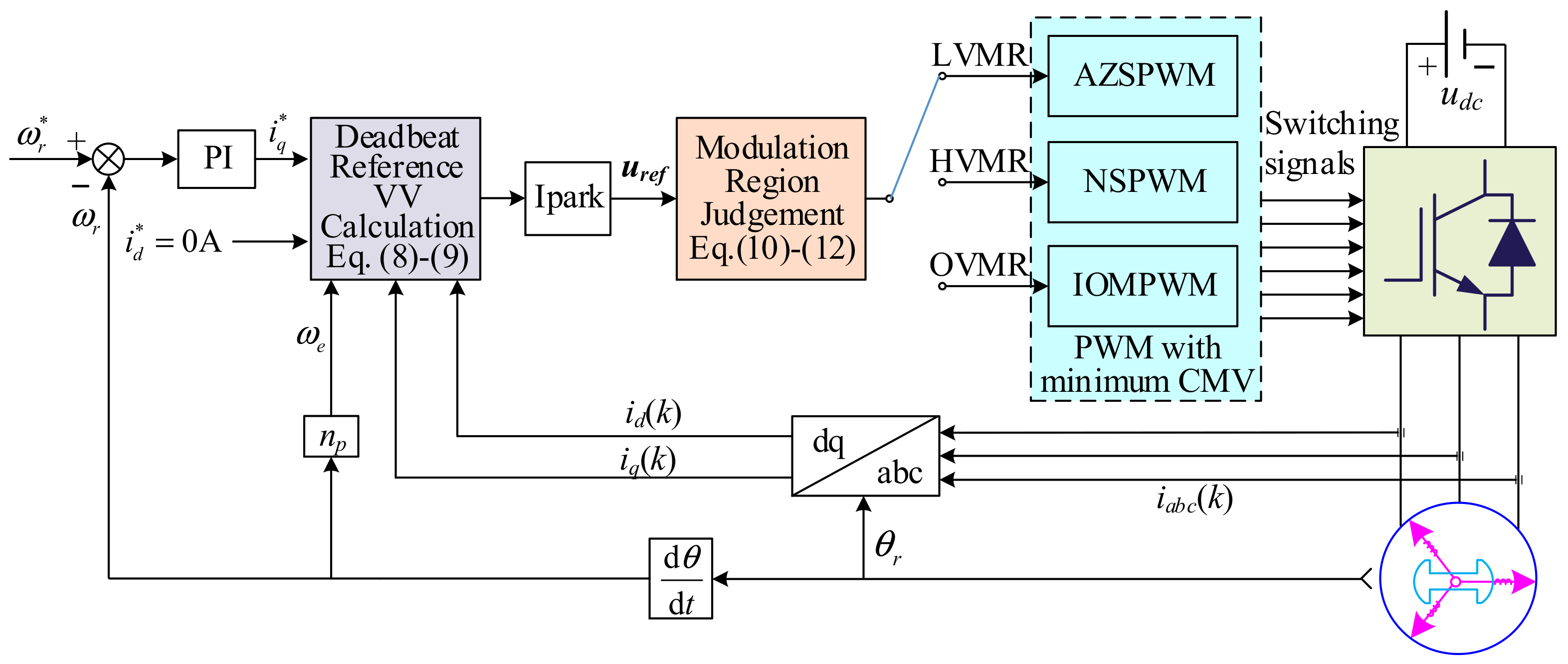
Figure 3.
Block diagram of the proposed modulation predict vector control scheme.
Figure 3.
Block diagram of the proposed modulation predict vector control scheme.
Figure 4.
Voltage linearity regions. (a) SVPWM, AZSPWM. (b) NSPWM. (c) RSPWM1–2. (d) RSPWM3.
Figure 4.
Voltage linearity regions. (a) SVPWM, AZSPWM. (b) NSPWM. (c) RSPWM1–2. (d) RSPWM3.
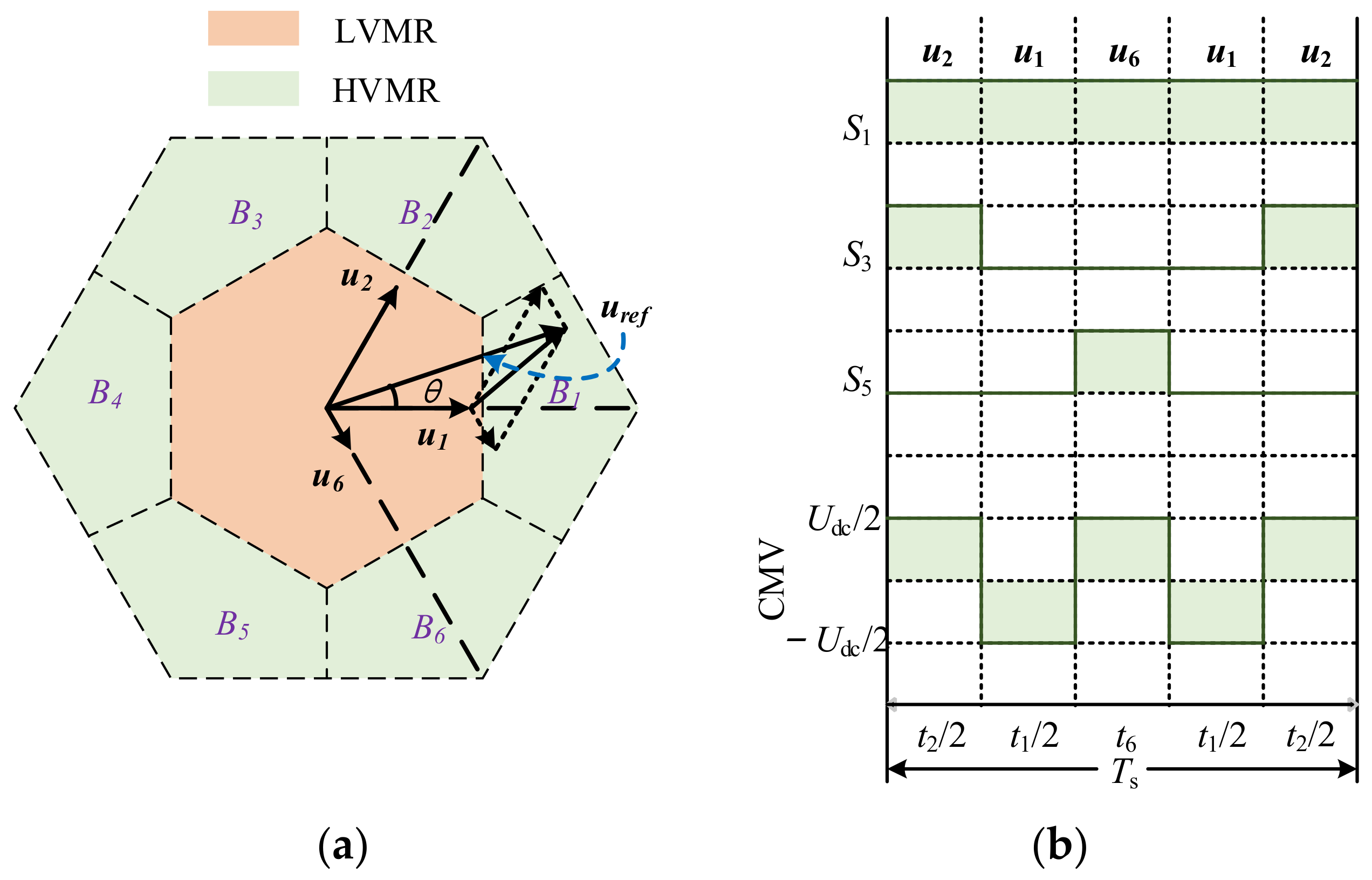
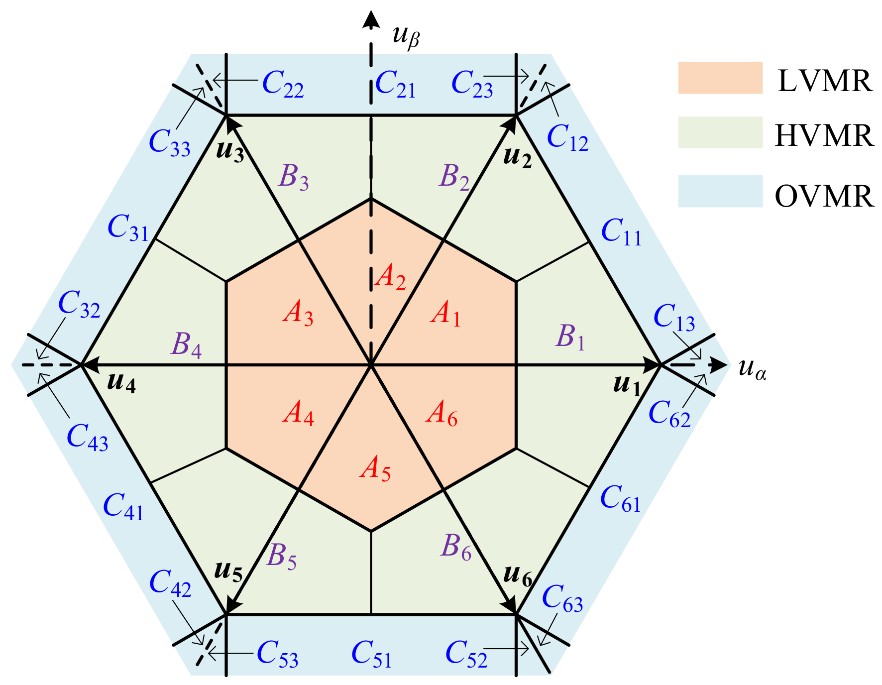
Figure 5.
Modulation region division of the improved modulation scheme.
Figure 5.
Modulation region division of the improved modulation scheme.
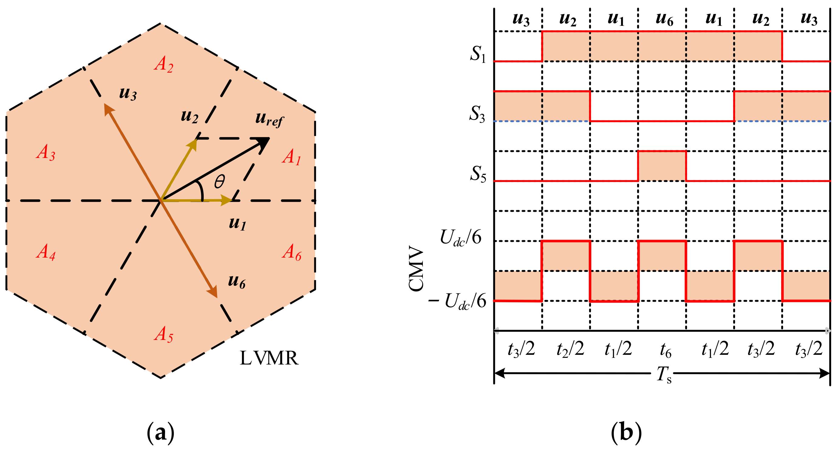
Figure 6.
The diagram of AZSPWM: (a) Zone division of LVMR; (b) Switching signal and CMV when uref is located in A1.
Figure 6.
The diagram of AZSPWM: (a) Zone division of LVMR; (b) Switching signal and CMV when uref is located in A1.
Figure 7.
The diagram of NSPWM: (a) Zone division of HVMR; (b) Switching signal and CMV when uref is in B1.
Figure 7.
The diagram of NSPWM: (a) Zone division of HVMR; (b) Switching signal and CMV when uref is in B1.
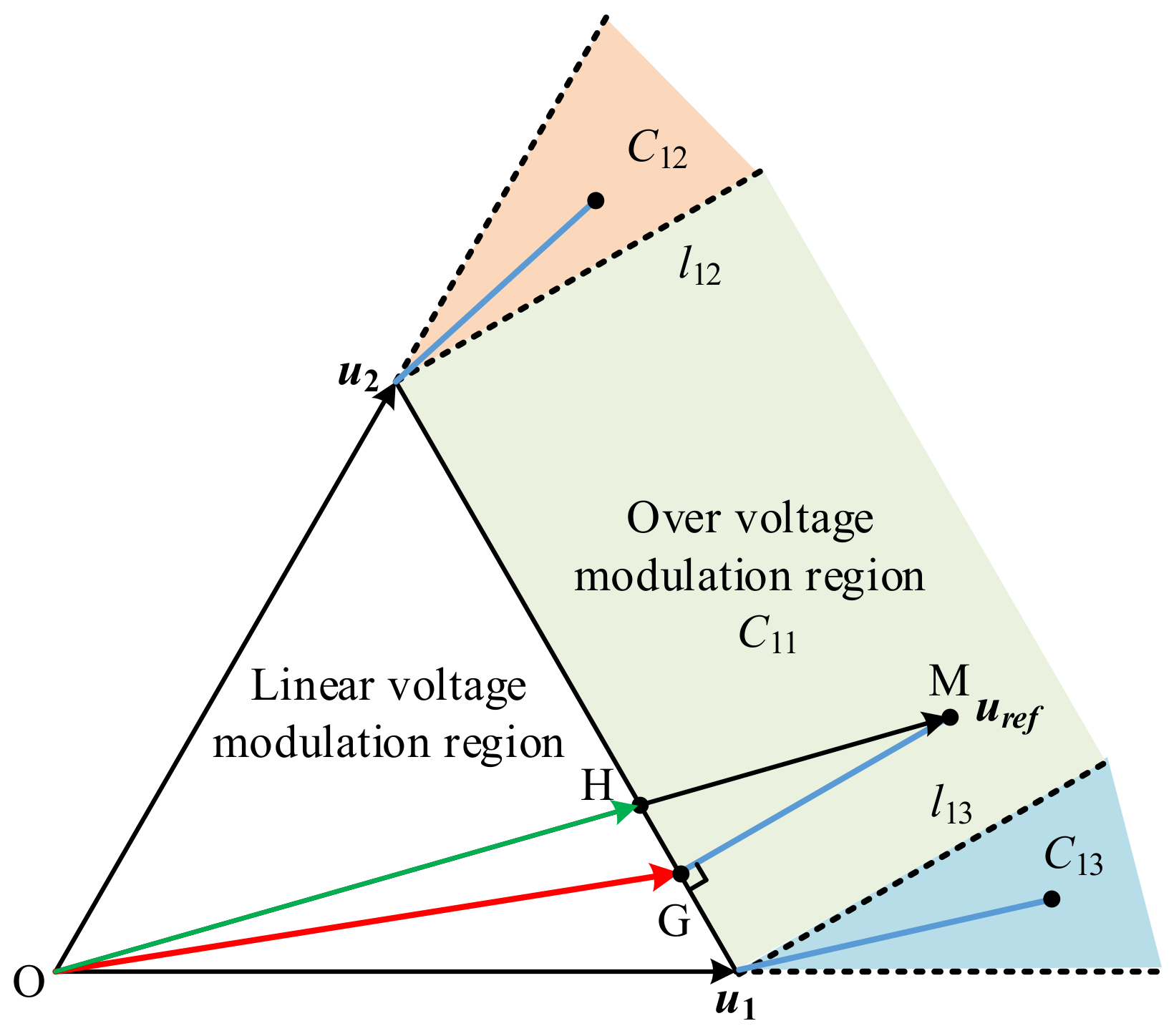
Figure 8.
The diagram of OVMR.
Figure 8.
The diagram of OVMR.
Figure 9.
Steady-state simulation results for AZSPWM when PMSM at 200 rpm with the load of 5 N·m. (a) Current and FFT analysis. (b) CMV. (c) Torque and speed.
Figure 9.
Steady-state simulation results for AZSPWM when PMSM at 200 rpm with the load of 5 N·m. (a) Current and FFT analysis. (b) CMV. (c) Torque and speed.
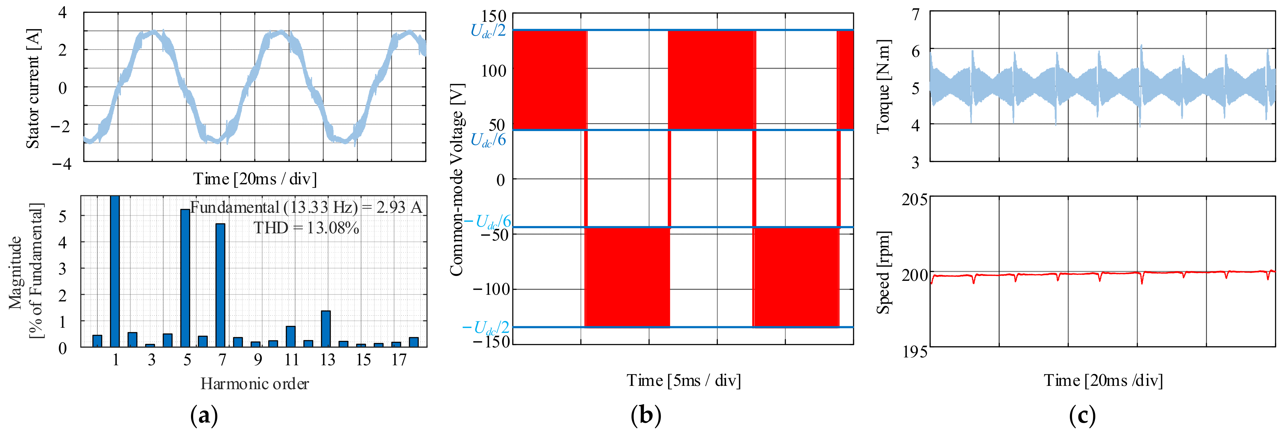
Figure 10.
Steady-state simulation results for NSPWM when PMSM at 200 rpm with the load of 5 N·m. (a) Current and FFT analysis. (b) CMV. (c) Torque and speed.
Figure 10.
Steady-state simulation results for NSPWM when PMSM at 200 rpm with the load of 5 N·m. (a) Current and FFT analysis. (b) CMV. (c) Torque and speed.
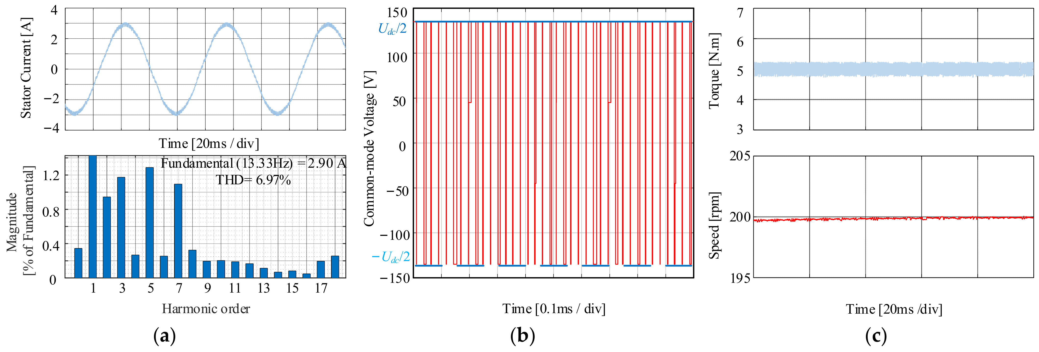
Figure 11.
Steady-state simulation results for SVPWM when PMSM at 200 rpm with the load of 5 N·m. (a) Current and FFT analysis. (b) CMV. (c) Torque and speed.
Figure 11.
Steady-state simulation results for SVPWM when PMSM at 200 rpm with the load of 5 N·m. (a) Current and FFT analysis. (b) CMV. (c) Torque and speed.
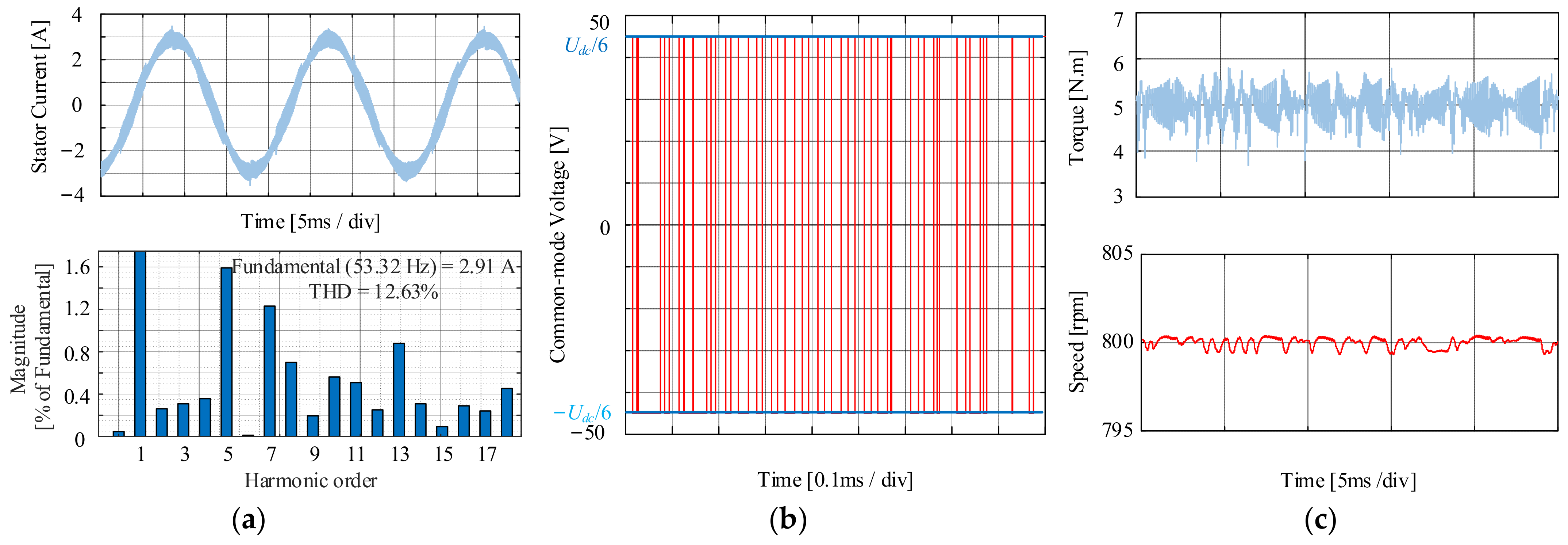
Figure 12.
Steady-state simulation results under NSPWM when PMSM at 800 rpm with the load of 5 N·m. (a) Current and FFT analysis. (b) CMV. (c) Torque and speed.
Figure 12.
Steady-state simulation results under NSPWM when PMSM at 800 rpm with the load of 5 N·m. (a) Current and FFT analysis. (b) CMV. (c) Torque and speed.
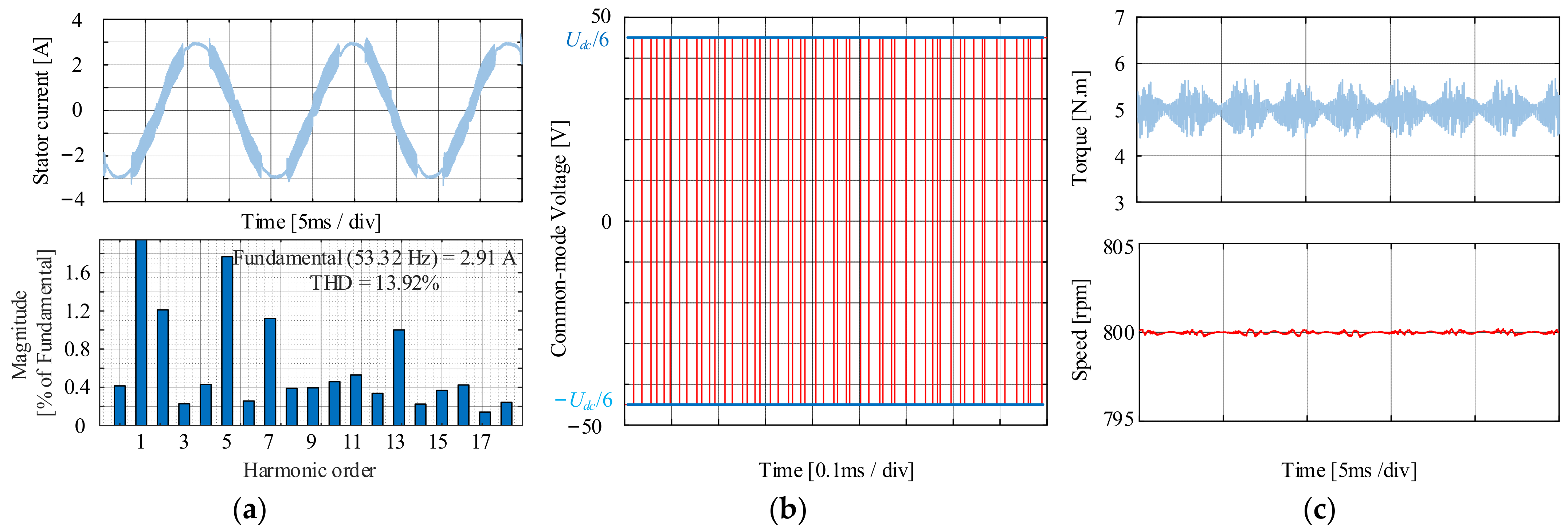
Figure 13.
Steady-state simulation results under AZSPWM when PMSM at 800 rpm with the load of 5 N·m. (a) Current and FFT analysis. (b) CMV. (c) Torque and speed.
Figure 13.
Steady-state simulation results under AZSPWM when PMSM at 800 rpm with the load of 5 N·m. (a) Current and FFT analysis. (b) CMV. (c) Torque and speed.
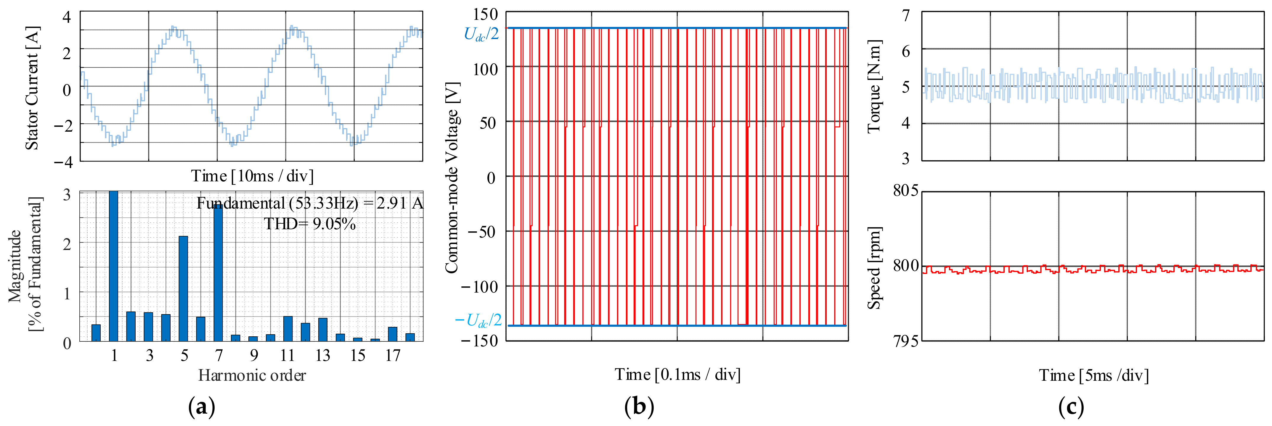
Figure 14.
Steady-state simulation results for SVPWM when PMSM at 800 rpm with the load of 5 N·m. (a) Current and FFT analysis. (b) CMV. (c) Torque and speed.
Figure 14.
Steady-state simulation results for SVPWM when PMSM at 800 rpm with the load of 5 N·m. (a) Current and FFT analysis. (b) CMV. (c) Torque and speed.
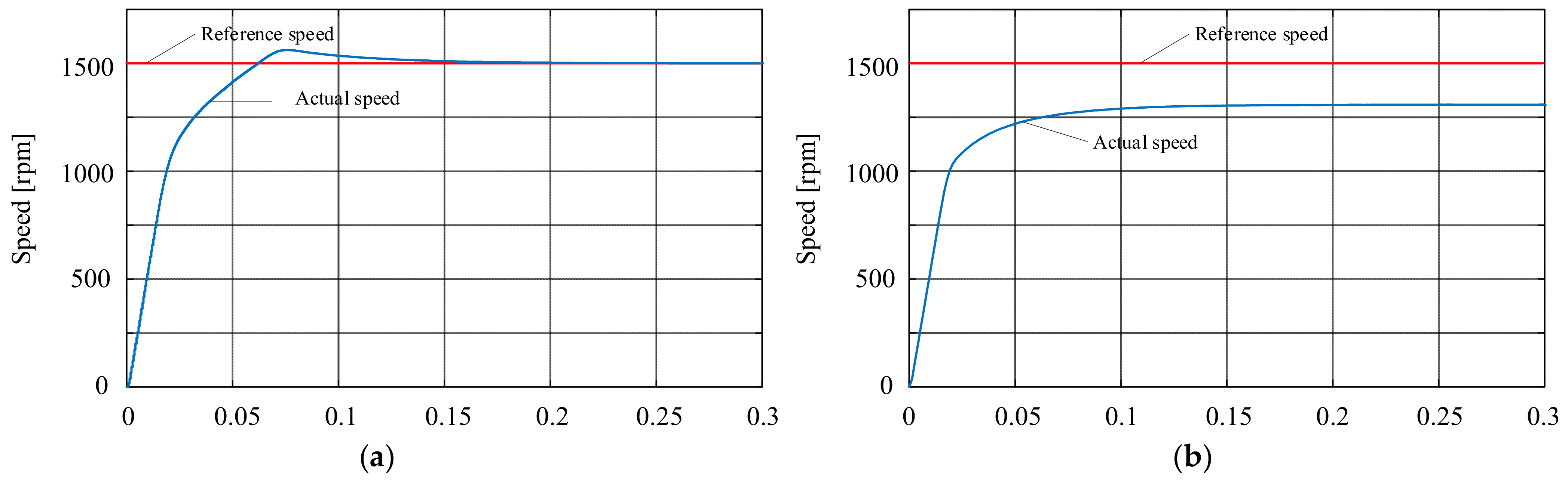
Figure 15.
Harsh start-up simulation dynamic analysis at 210 V (DC-link voltage) and 1500 rpm (Control speed). (a). The proposed method. (b). Traditional overvoltage modulation method.
Figure 15.
Harsh start-up simulation dynamic analysis at 210 V (DC-link voltage) and 1500 rpm (Control speed). (a). The proposed method. (b). Traditional overvoltage modulation method.
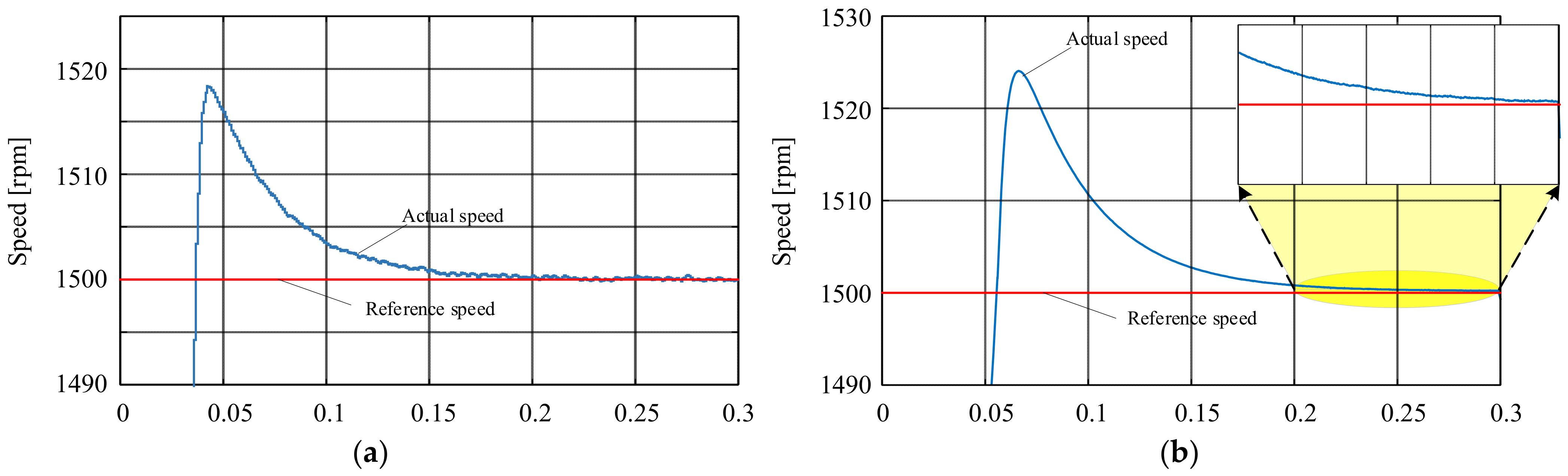
Figure 16.
Start-up simulation steady-state analysis at 270 V (DC-link voltage) and 1500 rpm (Control speed). (a). The proposed method. (b). Traditional overvoltage modulation method.
Figure 16.
Start-up simulation steady-state analysis at 270 V (DC-link voltage) and 1500 rpm (Control speed). (a). The proposed method. (b). Traditional overvoltage modulation method.
Figure 17.
The improvement of IOMPWM.
Figure 17.
The improvement of IOMPWM.
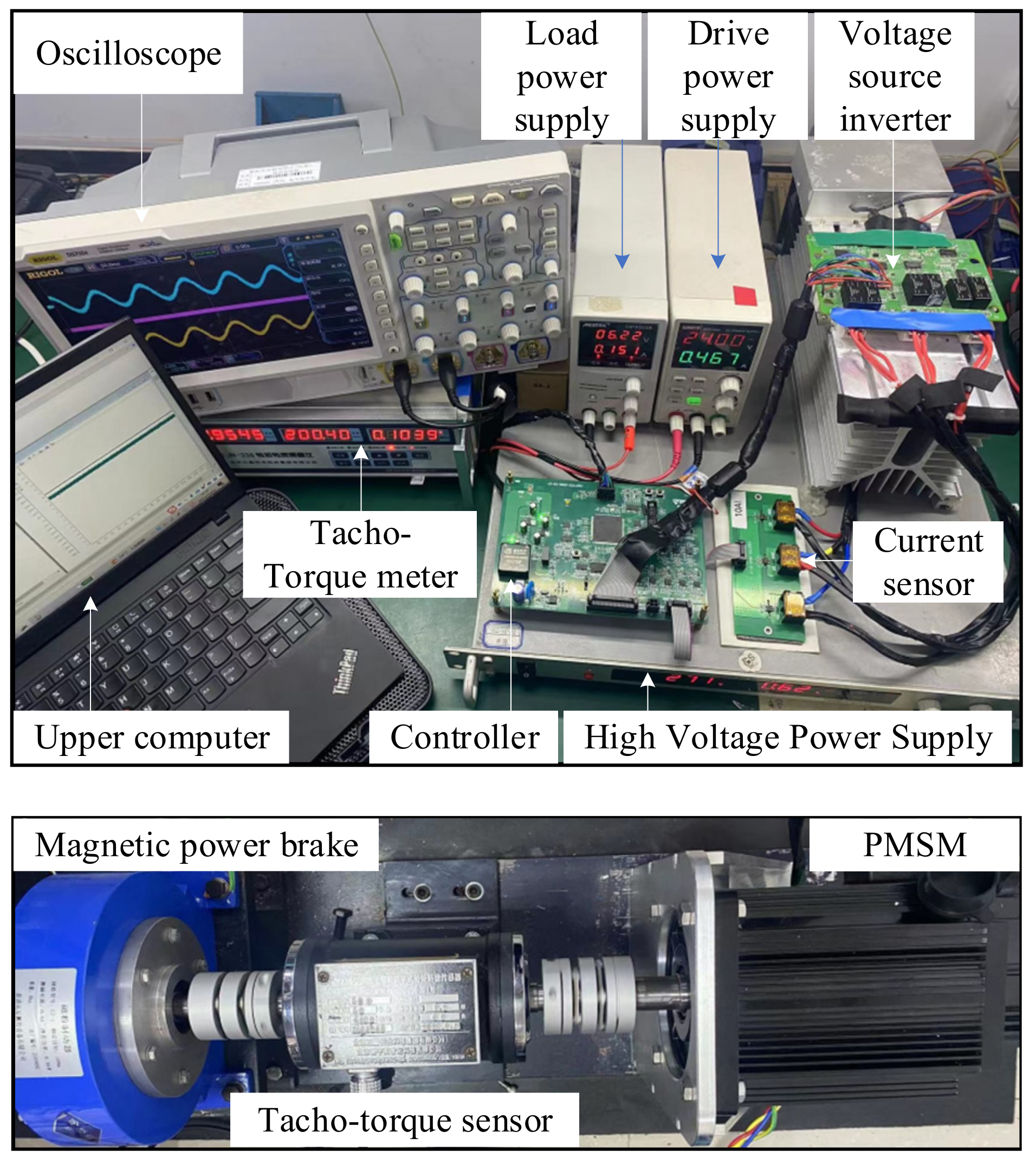
Figure 18.
Experimental platform of PMSM control system.
Figure 18.
Experimental platform of PMSM control system.
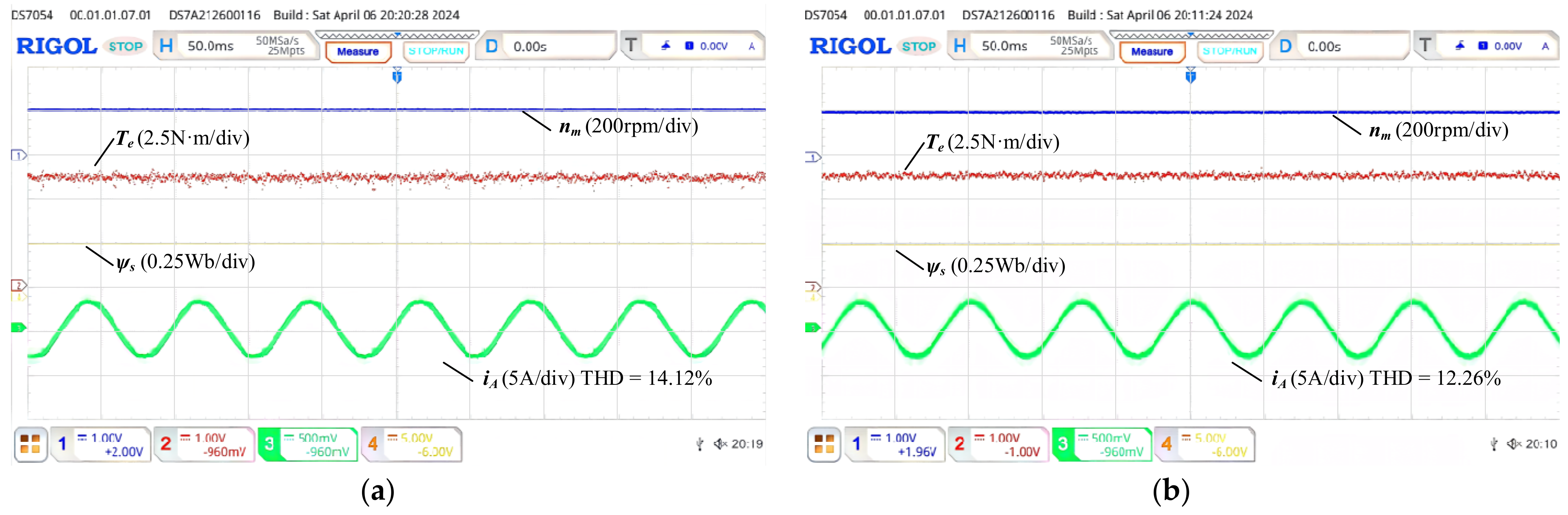
Figure 19.
Steady-state experimental results for the proposed method when PMSM at 200 rpm with the load of 5 N·m. (a) The proposed method. (b) SVPWM.
Figure 19.
Steady-state experimental results for the proposed method when PMSM at 200 rpm with the load of 5 N·m. (a) The proposed method. (b) SVPWM.
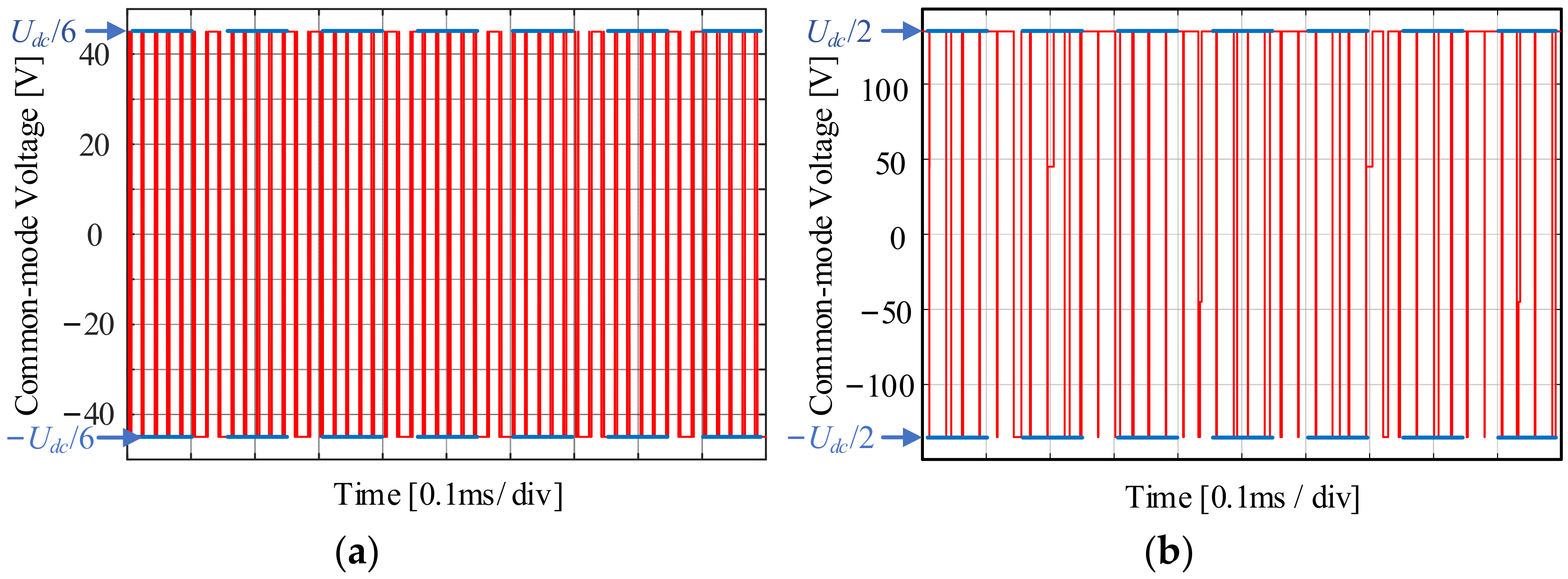
Figure 20.
CMV waveforms reconstructed based on the switching signals when PMSM at 200 rpm with the load of 5 N·m. (a) The proposed method. (b) SVPWM.
Figure 20.
CMV waveforms reconstructed based on the switching signals when PMSM at 200 rpm with the load of 5 N·m. (a) The proposed method. (b) SVPWM.
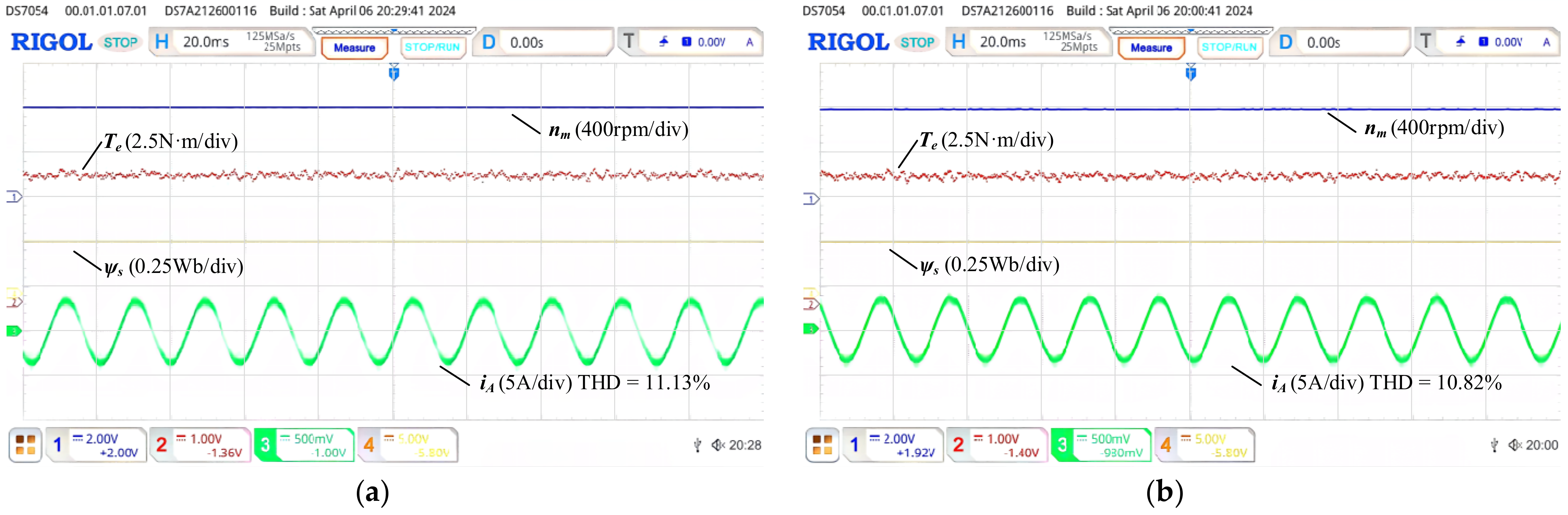
Figure 21.
Steady-state experimental results under AZSPWM when PMSM at 800 rpm with the load of 5 N·m. (a) The proposed method. (b) SVPWM.
Figure 21.
Steady-state experimental results under AZSPWM when PMSM at 800 rpm with the load of 5 N·m. (a) The proposed method. (b) SVPWM.
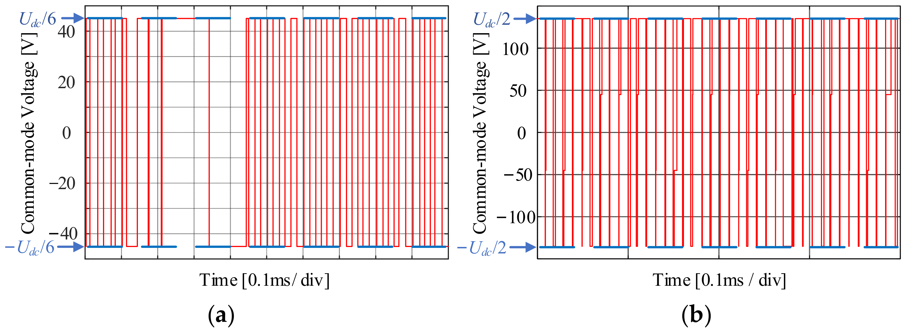
Figure 22.
CMV waveforms reconstructed based on the switching signals when PMSM operates at 800 rpm with the load of 5 N·m. (a) The proposed method. (b) SVPWM.
Figure 22.
CMV waveforms reconstructed based on the switching signals when PMSM operates at 800 rpm with the load of 5 N·m. (a) The proposed method. (b) SVPWM.
Figure 23.
Dynamic response experimental results with a load of 5 N·m accelerate from 200 rpm to 800 rpm. (a) The proposed method. (b) SVPWM.
Figure 23.
Dynamic response experimental results with a load of 5 N·m accelerate from 200 rpm to 800 rpm. (a) The proposed method. (b) SVPWM.
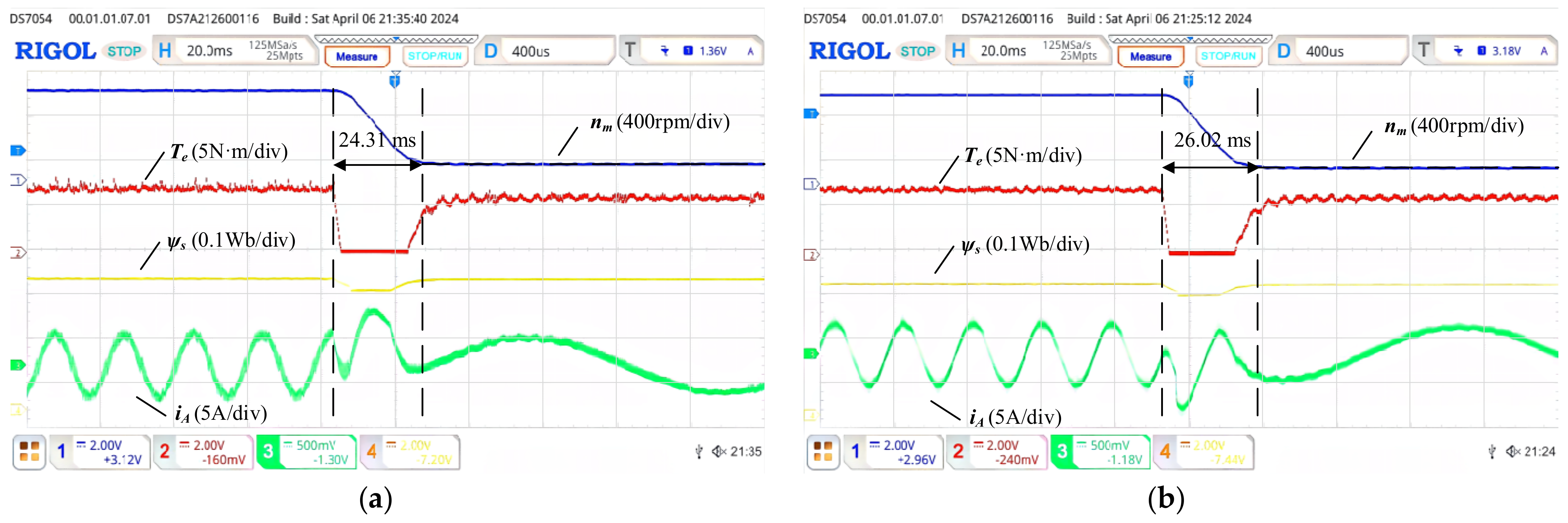
Figure 24.
Dynamic response experimental results with a load of 5 N·m decelerate from 800 rpm to 200 rpm. (a) The proposed method. (b) SVPWM.
Figure 24.
Dynamic response experimental results with a load of 5 N·m decelerate from 800 rpm to 200 rpm. (a) The proposed method. (b) SVPWM.
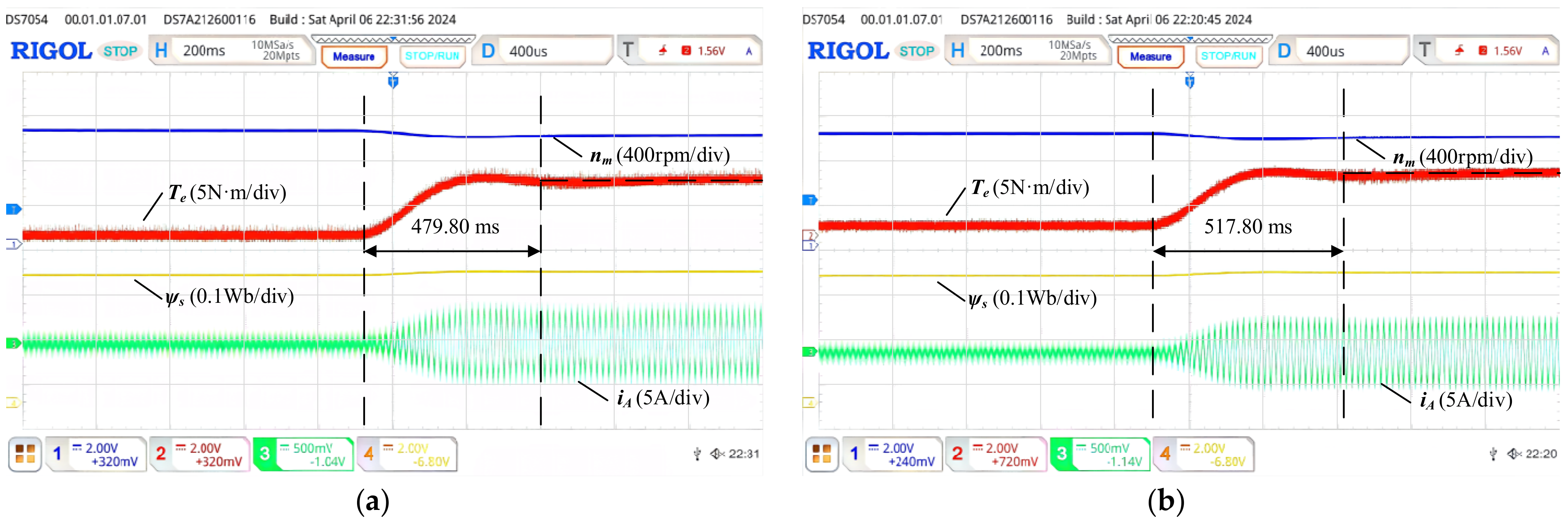
Figure 25.
Dynamic response experimental results at 1000 rpm increase from 0 N·m to 5 N·m. (a) The proposed method. (b) SVPWM.
Figure 25.
Dynamic response experimental results at 1000 rpm increase from 0 N·m to 5 N·m. (a) The proposed method. (b) SVPWM.
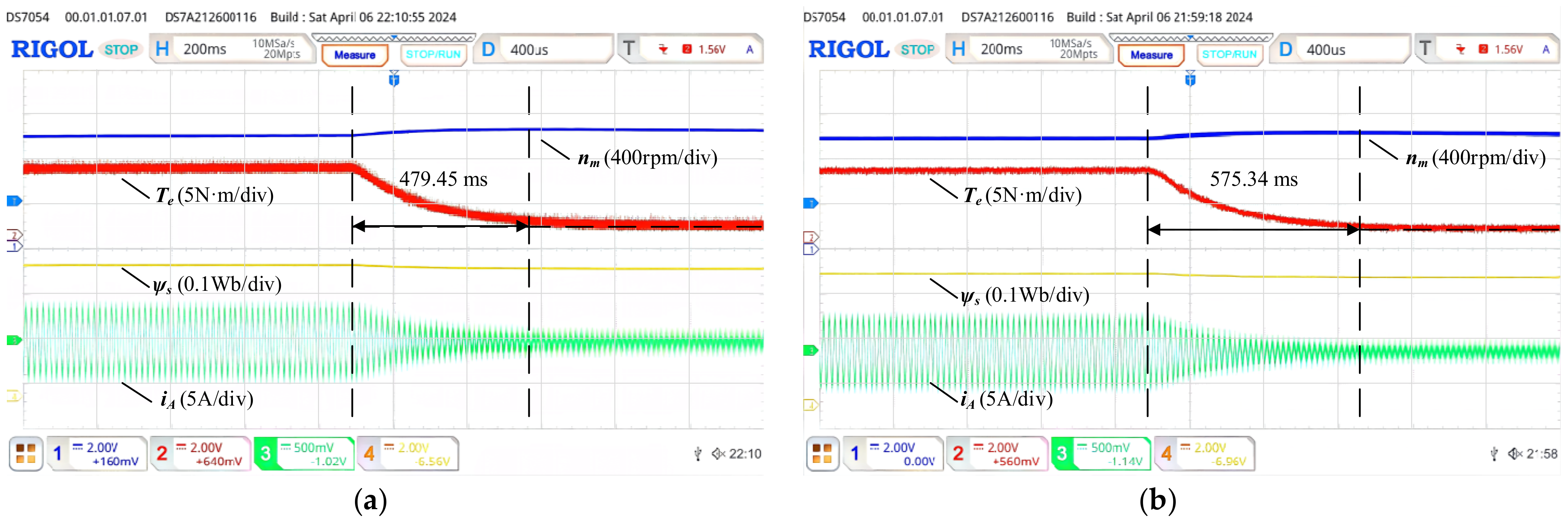
Figure 26.
Dynamic response experimental results at 1000 rpm decrease from 5 N·m to 0 N·m. (a) The proposed method. (b) SVPWM.
Figure 26.
Dynamic response experimental results at 1000 rpm decrease from 5 N·m to 0 N·m. (a) The proposed method. (b) SVPWM.
Table 1.
Eight basic VVs’ CMV magnitude for SVPWM.
Table 1.
Eight basic VVs’ CMV magnitude for SVPWM.
| Voltage Vector | Switching Sequence | CMV Magnitude |
|---|
| u0 | (0,0,0) | −Udc/2 |
| u1 | (1,0,0) | −Udc/6 |
| u2 | (1,1,0) | Udc/6 |
| u3 | (0,1,0) | −Udc/6 |
| u4 | (0,1,1) | Udc/6 |
| u5 | (0,0,1) | −Udc/6 |
| u6 | (1,0,1) | Udc/6 |
| u7 | (1,1,1) | Udc/2 |
Table 2.
Synthesized AVVs with dwell time for uref in all zones of LVMR.
Table 2.
Synthesized AVVs with dwell time for uref in all zones of LVMR.
| Zone | Applied 1st VV with Dwell Time | Applied 2nd VV with Dwell Time | Applied 3rd VV with Dwell Time | Applied 4th VV with Dwell Time |
|---|
| A1 | u1, t1 = MTssin(π/3 − θ) | u2, t2 = MTssin(θ) | u3 | u6 |
| A2 | u2, t2 = MTssin(2π/3 − θ) | u3, t3 = MTssin(θ − π/3) | u4 | u1 |
| A3 | u3, t3 = MTssin(θ) | u4, t4 = MTssin(θ − 2π/3) | u5 | u2 |
| A4 | u4, t4 = MTssin(θ + π/3) | u5, t5 = −MTssin(θ) | u6 | u3 |
| A5 | u5, t5 = MTssin(θ + 2π/3) | u6, t6 = MTssin(θ + 2π/3) | u1 | u4 |
| A6 | u6, t6 = −MTssin(θ) | u1, t1 = MTssin(θ + π/3) | u2 | u5 |
Table 3.
Synthesized AVVs with dwell time for uref in all zones of HVMR.
Table 3.
Synthesized AVVs with dwell time for uref in all zones of HVMR.
| Zone | uleft and tleft | umiddle and tmiddle | uright and tright |
|---|
| B1 | u2, t2 | u1, t1 | u6, t6 |
| B2 | u3, t3 | u2, t3 | u1, t1 |
| B3 | u4, t4 | u3, t2 | u2, t2 |
| B4 | u5, t5 | u4, t6 | u3, t3 |
| B5 | u6, t6 | u5, t4 | u4, t4 |
| B6 | u1, t1 | u6, t5 | u5, t5 |
Table 4.
Synthesized AVVs with dwell time for uref in all zones of OVMR.
Table 4.
Synthesized AVVs with dwell time for uref in all zones of OVMR.
| Sector | Zone | Applied 1st VV with Dwell Time | Applied 2nd VV with Dwell Time |
|---|
| I | C11 | u1 | u2, t2= Ts − t1 |
| C12 | u2, t2= Ts | No |
| C13 | u1, t1= Ts | No |
| II | C21 | u2 | u3, t3= Ts − t2 |
| C22 | u3, t3= Ts | No |
| C23 | u2, t2= Ts | No |
| III | C31 | u3 | u4, t4= Ts − t2 |
| C32 | u4, t4= Ts | No |
| C33 | u3, t3= Ts | No |
| IV | C41 | u4 | u5, t2= Ts − t1 |
| C42 | u5, t5= Ts | No |
| C43 | u4, t4= Ts | No |
| V | C51 | u5 | u5, t3= Ts − t2 |
| C52 | u6, t6= Ts | No |
| C53 | u5, t5= Ts | No |
| VI | C61 | u6 | u1, t1= Ts − t2 |
| C62 | u1, t1= Ts | No |
| C63 | u6, t6= Ts | No |
Table 5.
Modulation accuracy ratio for uref in all zones of OVMR.
Table 5.
Modulation accuracy ratio for uref in all zones of OVMR.
| Sector | Zone | IOMPWM | Conventional Method |
|---|
| I | C11 | | |
| C12 | |
| C13 |
| II | C21 | | |
| C22 | |
| C23 |
| III | C31 | | |
| C32 | |
| C33 |
| IV | C41 | | |
| C42 | |
| C43 |
| V | C51 | | |
| C52 | |
| C53 |
| VI | C61 | | |
| C62 | |
| C63 |
Table 6.
Parameters of PMSM.
Table 6.
Parameters of PMSM.
| Parameters | Description | Value |
|---|
| Rs (Ω) | Stator resistance | 1.443 |
| Ld (mH) | d-axis inductance | 5.541 |
| Lq (mH) | q-axis inductance | 5.541 |
| ψf (Web) | Flux linkage | 0.2852 |
| iN (A) | Rated current | 4.5 |
| nN (r/min) | Rated speed | 1000 |
| TN (N·m) | Rated toque | 10 |
| np | Pole pairs | 4 |
| J (kg.m2) | Rotational inertia | 0.00194 |
| Udc (V) | DC-bus voltage | 270 |
| fS (Hz) | Carrier frequency | 10,000 |
Table 7.
Steady-state simulation results summary table.
Table 7.
Steady-state simulation results summary table.
| Method | Operation | Current THD | Torque Ripple | CMV Magnitude |
|---|
| AZSPWM | 200 rpm; 5 N·m | 15.17% | 0.2688 N·m | 46.67 V |
| 800 rpm; 5 N·m | 13.92% | 0.2777 N·m | 46.67 V |
| NSPWM | 200 rpm; 5 N·m | 13.08% | 0.1603 N·m | 135.0 V |
| 800 rpm; 5 N·m | 12.63% | 0.2283 N·m | 46.67 V |
| SVPWM | 200 rpm; 5 N·m | 6.97% | 0.1076 N·m | 135.0 V |
| 800 rpm; 5 N·m | 9.05% | 0.1886 N·m | 135.0 V |
Table 8.
Steady-state experiment results summary table.
Table 8.
Steady-state experiment results summary table.
| Region | Method | Current THD | Torque Ripple | CMV Magnitude |
|---|
| LVMR | The proposed method | 14.12% | 0.0614 N·m | 46.67 V |
| SVPWM | 12.26% | 0.0428 N·m | 135.0 V |
| HVMR | The proposed method | 11.13% | 0.0564 N·m | 46.67 V |
| SVPWM | 10.82% | 0.0515 N·m | 135.0 V |
Table 9.
Dynamic experiment results summary table.
Table 9.
Dynamic experiment results summary table.
| Operation Condition | The Proposed Method | SVPWM |
|---|
| Speed Step | 200–800 rpm | 45.21 ms | 48.49 ms |
| 800–200 rpm | 24.31 ms | 26.02 ms |
| Load Step | 0–5 N·m | 479.80 ms | 517.80 ms |
| 5–0 N·m | 479.45 ms | 575.34 ms |


