Article

Degradation-Sensitive Control Algorithm Based on Phase Optimization for Interleaved DC–DC Converters

1
School of Electrical and Electronics Engineering, Chung-Ang University, Seoul 06974, Republic of Korea
2
Department of Electrical and Computer Engineering, Mississippi State University, Starkville, MS 39762, USA
*
Authors to whom correspondence should be addressed.
Machines 2023, 11(6), 624; https://doi.org/10.3390/machines11060624
Submission received: 1 May 2023 / Revised: 29 May 2023 / Accepted: 30 May 2023 / Published: 5 June 2023
(This article belongs to the Section Electrical Machines and Drives)

Abstract

:
As the use of interleaved DC–DC converters in electric vehicles (EVs) increases, research on reliability improvement is required. In the case of interleaved DC–DC converters, degradation occurs between transistors and capacitors. In particular, transistor degradation imbalances cause an increase in output capacitor RMS current, which increases power loss and accelerates capacitor degradation. This degradation affects system reliability by increasing thermal stress. In this paper, based on a degraded 2-leg interleaved DC–DC boost converter, research to reduce the converter’s output capacitor RMS current was conducted. The output capacitor RMS current according to the transistor degradation imbalance was analyzed. As a result, it was confirmed that the transistor degradation imbalance causes an increase in the capacitor RMS current. To address this issue, a phase optimization algorithm for reducing increased capacitor RMS current is presented in this paper. Next, the phase optimization algorithm is mathematically analyzed. Finally, its efficacy is proved through simulations and experiments.

1. Introduction

Numerous studies are being conducted to enhance the efficiency and performance of DC–DC converters. For increasing their efficiency, interleaved DC–DC converters are being actively developed. Interleaved DC–DC converters are being actively used to increase converter efficiency, and various topologies have been developed, including interleaved buck, boost, buck–boost, SEPIC, and the Cuk converter [1,2,3]. The interleaved buck converter is used to step down the voltage, the interleaved boost converter is used to step up the voltage, and the interleaved buck–boost is a hybrid of the two. The interleaved SEPIC and Cuk converters have a structure in which an additional capacitor is connected between the input inductor and the output terminal. A number of inductors can be connected to the input terminal of interleaved DC–DC converters. In addition, currents with different phases flow through the legs to which the inductors are connected. Interleaved converters are generally used in two forms: 2-leg and 3-leg. Furthermore, they have the advantages of reduced inductor size and increased switching frequency. However, interleaved DC–DC converters require more transistors compared to conventional DC–DC converters, meaning degradation in terms of imbalance can occur between the transistors. This degradation imbalance increases the thermal stress of certain transistors, which can result in system failure. When transistors fail, a gate-source short or drain-source short can occur, which affect other circuit components and the entire power conversion system. Moreover, degradation not only occurs in transistors but also in capacitors. When capacitors are degraded, the equivalent series resistance (ESR) value increases. As a result, the increased ESR causes a decrease in efficiency and reliability of the system. Thus, the degradation of transistors and capacitors increases their power losses, accelerating the degradation. Accordingly, since interleaved DC–DC converters are mainly used in mobility systems, research has been actively conducted on improving their reliability [4,5,6,7].
Transistors and capacitors are generally considered the main causes of failure in converters [4,8]. To estimate the degradation state of transistors and capacitors, loss models and thermal models have been proposed. In addition, various studies have been conducted to estimate their reliability in online and offline systems [4,5,6,7,8,9,10,11,12,13,14,15]. Furthermore, the development of control algorithms to delay degradation is ongoing [15,16,17,18]. Among these various algorithms, current magnitude control algorithms have mainly been developed that reduce power losses of the more degraded leg [17,18] in which less current flows in the degraded leg and more current flows in the other leg. However, when the current magnitude difference of each leg increases, the root mean square (RMS) current of the output capacitor increases. Moreover, when the converter has been operating for an extended period, degradation of the capacitors progresses similarly to transistors. Therefore, an increase in the capacitor RMS current results in an increased risk of capacitor failure.
In this paper, a phase optimization algorithm is proposed for reducing increased capacitor RMS current. The first stage is to derive a capacitor RMS current formula (including phase variables) through a mathematical analysis. After this, the phase is optimized through the MATLAB function. Then, the optimized phase is applied to the degraded interleaved converter. To apply the phase optimization algorithm, a 2-leg interleaved DC–DC boost converter based on a silicon-carbide metal-oxide-semiconductor-field-effect-transistor (SiC-MOSFET) is used. In the past, devices such as insulated gate bipolar transistors (IGBTs) have been widely used. However, the use of SiC-MOSFETs (which are wide-bandgap (WBG) transistors) is increasing. In SiC-MOSFETs, degradation occurs in its gate oxide layer and bond wire due to the high kinetic energy of the electrons and their deterioration during operation. Accordingly, to degrade the SiC-MOSFET, a high electric field (HEF) degradation experiment is performed [19,20]. Subsequently, the current magnitude of a specific leg is reduced by using a more degraded SiC-MOSFET. Next, the changes in capacitor RMS current according to current magnitude variations are analyzed. At this time, the capacitor RMS current varies depending on the phase. Finally, the proposed phase optimization algorithm is verified by applying the optimized phase conditions to experiments and simulations.
In Section 2, the characteristics of conventional 2-leg interleaved converters are analyzed, and a mathematical analysis of the phase optimization algorithm is conducted in Section 3. In Section 4, the results of applying the proposed phase optimization algorithm to a simulation are analyzed. Finally, the experimental results and conclusions are presented in Section 5 and Section 6, respectively.

2. Conventional Interleaved DC–DC Boost Converter

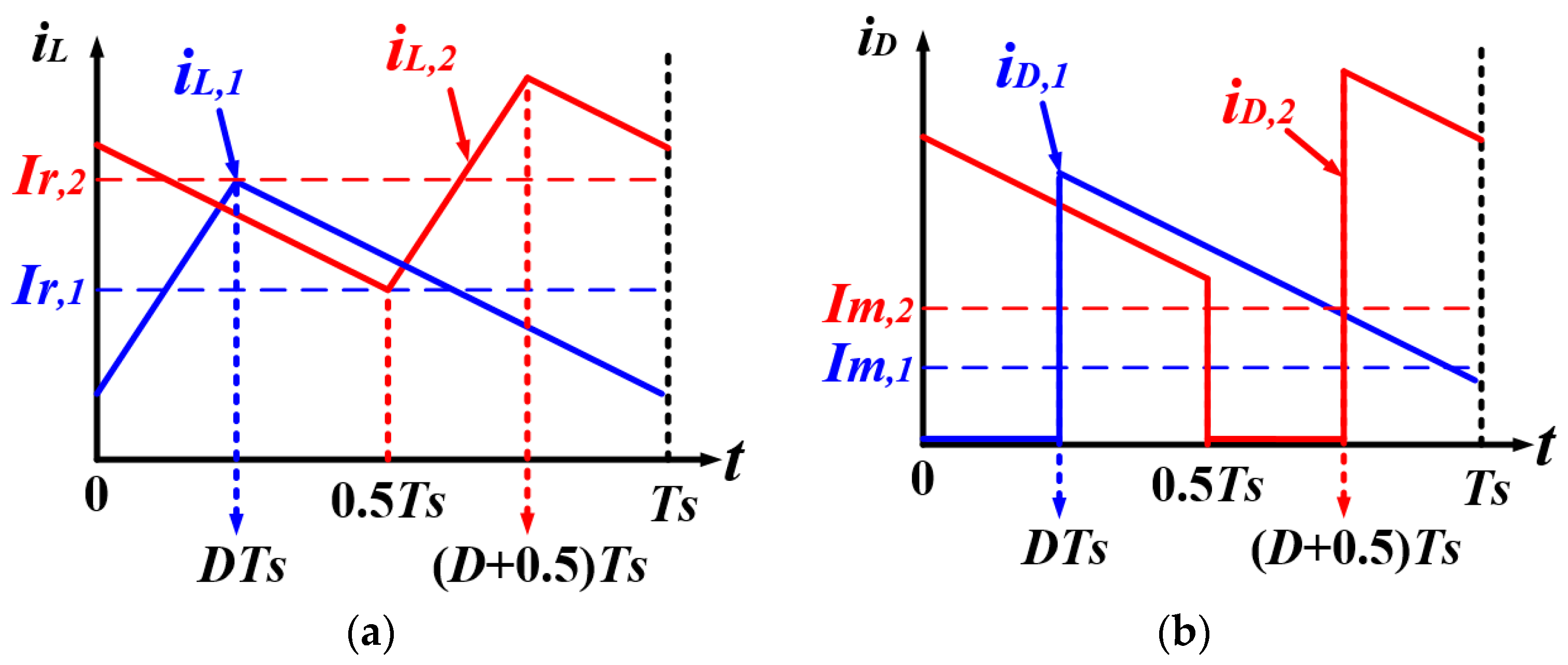
There are various interleaved converter topologies, such as interleaved buck, boost, buck–boost, SEPIC, and Cuk converters. In this paper, research is conducted on a 2-leg interleaved DC–DC boost converter. In conventional 2-leg interleaved DC–DC boost converters, two inductors are connected to the input side in parallel, and the input currents flowing through each inductor are controlled by transistors. Moreover, these currents have a phase difference of 180°. A circuit diagram of the converter used in this paper is displayed in Figure 1a. The line connected to L1 is termed L1-leg, while the line connected to L2 is termed L2-leg. The 2-leg interleaved converter uses two transistors, and the output voltage is controlled by adjusting their duty cycle (D). In Figure 1a, V i is input voltage, and V o is output voltage. The transistor and diode connected to the L1-leg are M1 and D1, and the transistor and diode connected to the L2-leg are M2 and D2. i L , 1 and i L , 2 are inductor currents of L1-leg and L2-leg, respectively. i D , 1 is the current flowing through D1, and i D , 2 is the current flowing through D2. i c and i o are output capacitor current and output load current, respectively. In interleaved DC–DC converters, the output voltage and inductor current are controlled by a digital signal processor, usually a proportional-integral (PI) controller. Next, the output value of the PI controller is compared with the carrier, and the generated switching signal is transmitted to the transistors (M1, M2) through the gate driver. In this paper, the converter operates in continuous conduction mode (CCM). The inductor current waveform of each leg is displayed in Figure 1b. One period of inductor current ( T S ) is the reciprocal of the switching frequency. For the L1-leg current, the transistor (M1) turns on, and the inductor current increases during the applied time ( D T S ) . Subsequently, from ( D T S ) to ( T S ), the transistor is turned off, and the inductor current decreases. In addition, a current that has a phase difference of 180° from the current of the L1-leg flows in the L2-leg. For the L2-leg current, transistor (M2) turns on at ( 0.5 T S ), and the inductor current increases during the applied time ( D T S ) . Subsequently, from ( D + 0.5 ) T S to ( 1.5 T S ), the transistor is turned off, and the inductor current decreases. Here, I r is the reference current value flowing through the inductor of each leg.
When degradation occurs in a specific leg of a transistor, thermal stress increases due to the increased drain-source on-resistance (Δ R D S ) . Since this can cause accelerated degradation of the transistor, methods for reducing the current magnitude of the degraded leg have been proposed. Figure 2a shows the inductor current waveform assuming that the L1-leg of the transistor is degraded. In addition, the inductance of each leg has the same value as L (i.e., L1 = L2 = L). To reduce power losses of the transistor in the L1-leg, the current magnitude is reduced, and the current magnitude of the L2-leg is increased by a corresponding value.
As demonstrated in Figure 2a, when the current magnitude of each leg changes by Δ I , the average current in each leg inductor ( I r , 1 , I r , 2 ) can be calculated using Equations (1) and (2).
I r , 1 = I r Δ I ,
I r , 2 = I r + Δ I .
When the duty cycle is less than 0.5, the expression for the inductor current of each leg displayed in Figure 2a is calculated as follows:
i L , 1 t = I r , 1 V i D 1 T S 2 L + V i t L , 0 t < D 1 T S I r , 1 + V i D 1 T S 2 L + V i V O t D 1 T S L , ( D 1 T S t < T S ) ,
i L , 2 t = I r , 2 + V i D 2 T S 2 L + ( V i V o ) ( 0.5 D 2 ) T S L + ( V i V O ) t L , 0 t < 0.5 T S I r , 2 V i D 2 T S 2 L + V i t 0.5 T S L 0.5 T S t < 0.5 + D 2 T s I r , 2 + V i D 2 T S 2 L + V i V o t L V i V o 0.5 + D 2 T S L 0.5 + D 2 t < T S ,
where V i is the input voltage, V o is the output voltage, D 1 is the duty cycle applied to the L1-leg of the transistor, and D 2 is the duty cycle applied to the L2-leg of the transistor.
Figure 2b shows the diode current waveform of each leg. Since the diode current only flows when the transistor is off, it is calculated as follows:
i D , 1 t = 0 , 0 t < D 1 T S I r , 1 + V i D 1 T S 2 L + V i V O t D 1 T S L , ( D 1 T S t < T S ) ,
i D , 2 t = I r , 2 + V i D 2 T S 2 L + ( V i V o ) ( 0.5 D 2 ) T S L + ( V i V O ) t L , 0 t < 0.5 T S 0 , 0.5 T S t < 0.5 + D 2 T s I r , 2 + V i D 2 T S 2 L + V i V o t L V i V o 0.5 + D 2 T S L , 0.5 + D 2 t < T S .
In addition, the average value of the diode current of each leg ( I m , x  (x = 1 or 2)) is calculated as follows:
I m , x = 1 T S 0 T S i D , x t d t .
Next, subtracting the average value of the diode in each leg (Equation (7)) from Equations (5) and (6), the capacitor current formula of each leg is calculated as follows:
i C , 1 t = I m , 1 , 0 t < D 1 T S I r , 1 + V i D 1 T S 2 L + V i V O t D 1 T S L I m , 1 , ( D 1 T S t < T S ) ,
i C , 2 t = I r , 2 + V i D 2 T S 2 L + ( V i V o ) ( 0.5 D 2 ) T S L + ( V i V O ) t L I m , 2 , 0 t < 0.5 T S I m , 2 , 0.5 T S t < 0.5 + D 2 T s I r , 2 + V i D 2 T S 2 L + V i V o t L V i V o 0.5 + D 2 T S L I m , 2 , 0.5 + D 2 t < T S .
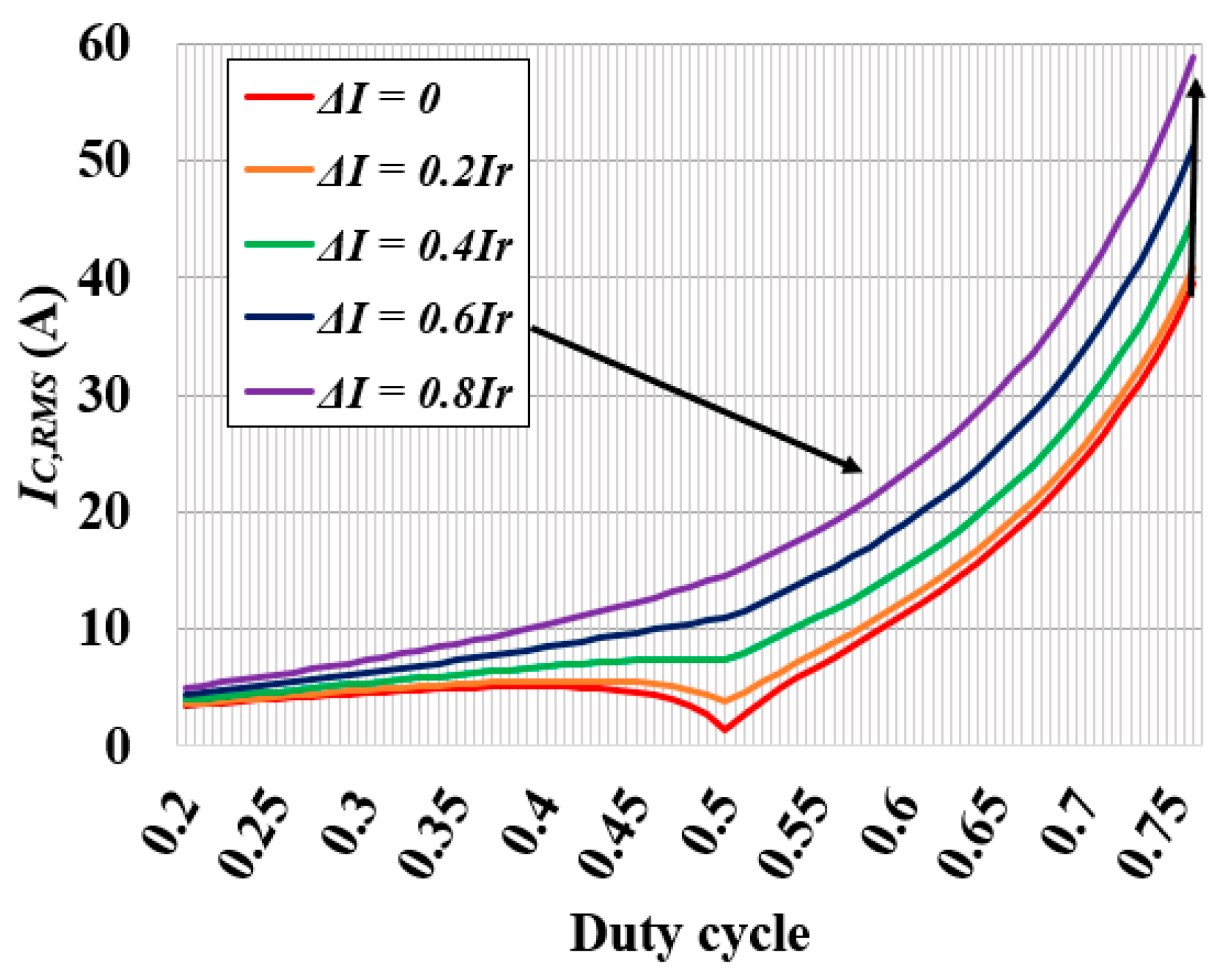
Equations (8) and (9) are the capacitor currents of each leg and are displayed in Figure 2c. The output capacitor RMS current ( I C , R M S ) is calculated with Equation (10) using Equations (8) and (9). Next, I C , R M S is calculated by increasing the current variation ( Δ I ) of each leg, as displayed in Figure 3.
I C , R M S = 1 T s 0 T s i C , 1 t + i C , 2 t 2 d t .
As demonstrated in Figure 3, as Δ I increases, I C , R M S also increases. Furthermore, the capacitor power loss ( P c a p ) is calculated as follows:
P c a p = E S R f × I C , R M S 2 ,
where E S R f is the equivalent resistance of the capacitor and depends on the frequency(f) [5,6,14]. Therefore, the increase in I C , R M S results in an increase in the capacitor power loss and thermal stress. In other words, increasing Δ I delays further degradation of the degraded transistors while accelerating the degradation of the output capacitor. As capacitor degradation progresses in accordance with the transistor, the accelerated degradation of the capacitor reduces the reliability of the system. To solve this problem, the next sections explain a phase optimization algorithm that minimizes increases in I C , R M S according to increases in Δ I .

3. Mathematical Analysis of Proposed Phase Optimization Algorithm

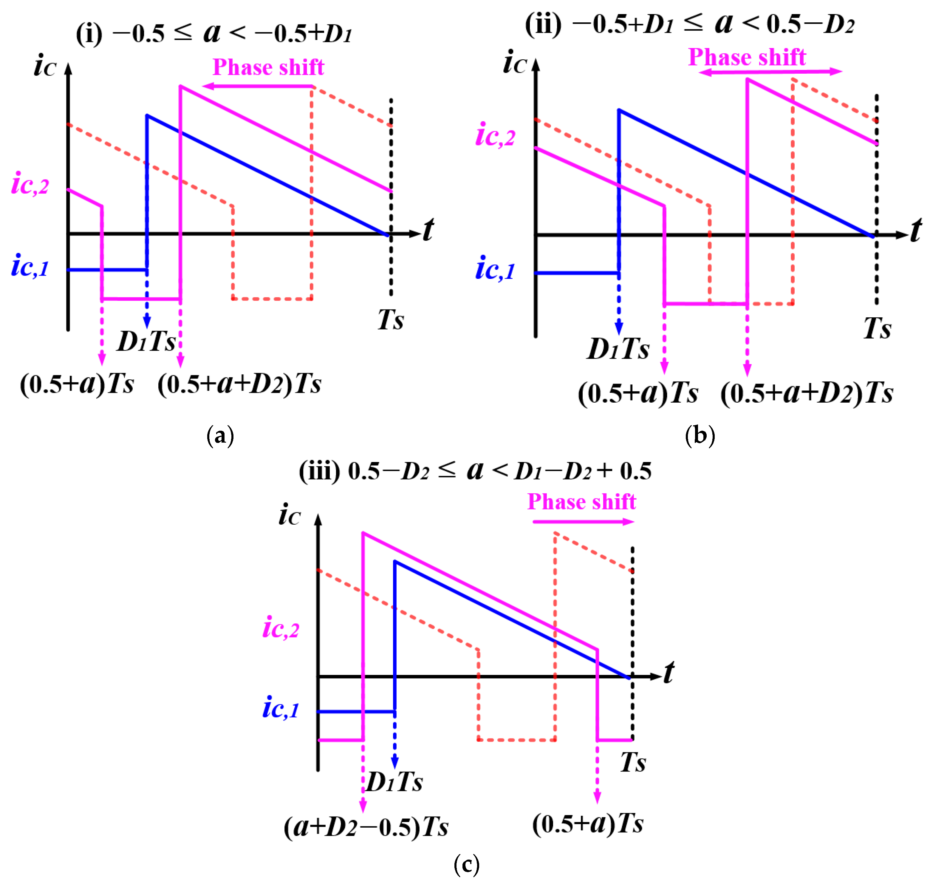
In this section, to reduce I C , R M S , a mathematical analysis of the optimization phase is explained when Δ I is increased. For this optimization, the phase of the L2-leg current is shifted by “ a ”  T s from the conventional phase (0.5 T s ) .   I C , R M S a is a formula that includes the phase variable “ a ” and is calculated using Equations (12)–(18). However, as demonstrated in Equations (12) and (13), “ i C , 1 t + i C , 2 a , t varies according to the amount of phase shift a  ×   T s . In other words, I C , R M S ( a ) is calculated as the square of Equation (13), and Equation (12) depends on the range of “ a ”. When D 1   and   D 2 are less than 0.5, the range of “ a ” is classified into the three intervals (i), (ii), and (iii), as shown in Figure 4. For example, since i C a , t = i C , 1 t + i C , 2 a , t has different values when t < D 1 T s , the integral interval must be different. Therefore, i C , 2 a , t and I C , R M S a in the three intervals are calculated using Equations (14)–(18).
I C , R M S ( a ) = 1 T s 0 T s i C a , t 2 d t ,
i C a , t = i C , 1 t + i C , 2 a , t ,
(i)
−0.5 a < −0.5 + D 1
i C , 2 ( a , t ) = I r , 2 + V i D 2 T S 2 L + ( V i V o ) ( 0.5 D 2 a ) T S L + ( V i V O ) t L I m , 2 , ( 0 t < a + 0.5 T S ) I m , 2 , ( ( a + 0.5 ) T S t < a + 0.5 + D 2 T s ) I r , 2 + V i D 2 T S 2 L + ( V i V o ) ( t a + 0.5 + D 2 T S ) L I m , 2 a + 0.5 + D 2 t < T S .
At −0.5 ≤ a < −0.5 + D 1 , the capacitor RMS current is calculated using Equations (8) and (12)–(14), which gives Equation (15).
I C , R M S a = 1 T s 0 0.5 + a T s i C a , t 2 d t + a + 0.5 T s D 1 T s i C a , t 2 d t + D 1 T s a + 0.5 + D 2 T s i C a , t 2 d t + a + 0.5 + D 2 T s T s i C a , t 2 d t 1 2 .
(ii)
−0.5 + D 1   a < 0.5 − D 2
At −0.5 + D 1 a < 0.5 − D 2 , using Equations (8) and (14), the capacitor RMS current is calculated through Equations (12) and (13), which gives Equation (16).
I C , R M S a = 1 T s 0 D 1 T s i C a , t 2 d t + D 1 T s a + 0.5 T s i C a , t 2 d t + a + 0.5 T s a + 0.5 + D 2 T s i C a , t 2 d t + a + 0.5 + D 2 T s T s i C a , t 2 d t 1 2 .
(iii)
0.5 – D 2   a < 0.5
At 0.5 − D 2 a < 0.5, using Equations (8) and (17), the capacitor RMS current is calculated through Equations (12) and (13), which gives Equation (18).
i C , 2 a , t = I m , 2 , 0 t < a + D 2 0.5 T S I r , 2 + V i D 2 T S 2 L + V i V o t a + D 2 0.5 T S L I m , 2 , a + D 2 0.5 T S t < a + 0.5 T s I m , 2 , a + 0.5 t < T S ,
I C , R M S a = 1 T s 0 a + D 2 0.5 T s i C a , t 2 d t + a + D 2 0.5 T D 1 T s i C a , t 2 d t + D 1 T s a + 0.5 T s i C a , t 2 d t + a + 0.5 T s T s i C a , t 2 d t 1 2 .
When the duty cycle is ≥0.5, the I C , R M S ( a ) formula can be derived in the same way as when the duty cycle is <0.5. When D 1 , D 2 are ≥0.5, the range of “a” is classified into three sections in the same way as when the duty cycle is <0.5. Therefore, the capacitor current I C , 2 a , t and the capacitor RMS current I C , R M S ( a ) in each section are calculated by Equations (15), (18), and (19). When the duty cycle is ≥0.5, like (i), I C , R M S ( a ) is calculated through Equations (8) and (12)–(15), at D 1 D 2 − 0.5 a < 0.5 − D 2 . Next, at 0.5 − D 2   a <   D 1 − 0.5, using Equations (8) and (18), which is the capacitor current, the capacitor RMS current is calculated using Equations (12) and (13), which is Equation (19).
I C , R M S a = 1 T s 0 a + D 2 0.5 T s i C a , t 2 d t + a + D 2 0.5 T ( a + 0.5 ) T s i C a , t 2 d t + ( a + 0.5 ) T s D 1 T s i C a , t 2 d t + D 1 T s T s i C a , t 2 d t 1 2 .
At D 1 − 0.5  a <   D 1 D 2 + 0.5, like (iii), using Equations (8) and (17), which is the capacitor current, the capacitor RMS current is calculated using Equations (12) and (13), which is Equation (18).
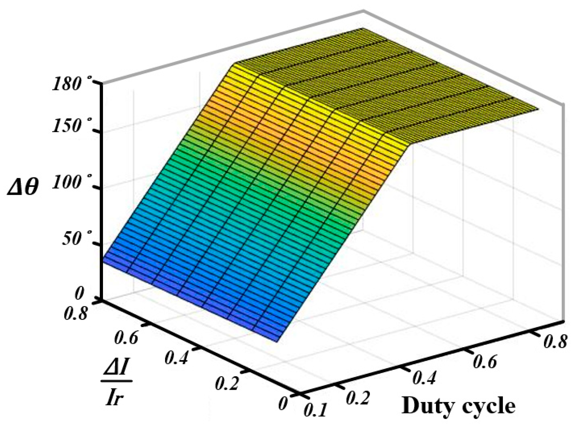
Based on the previous analysis, the optimized phase value, a , that minimizes the capacitor RMS current is obtained through a MATLAB function. Subsequently, the optimized phase value, a , is converted into degrees ( Δ θ ). The relationship between Δ θ and, a is then calculated using Equation (20). Here, Δ θ is the phase degree difference between the L1-leg and the L2-leg.
Δ θ = a + 0.5 360 ° .
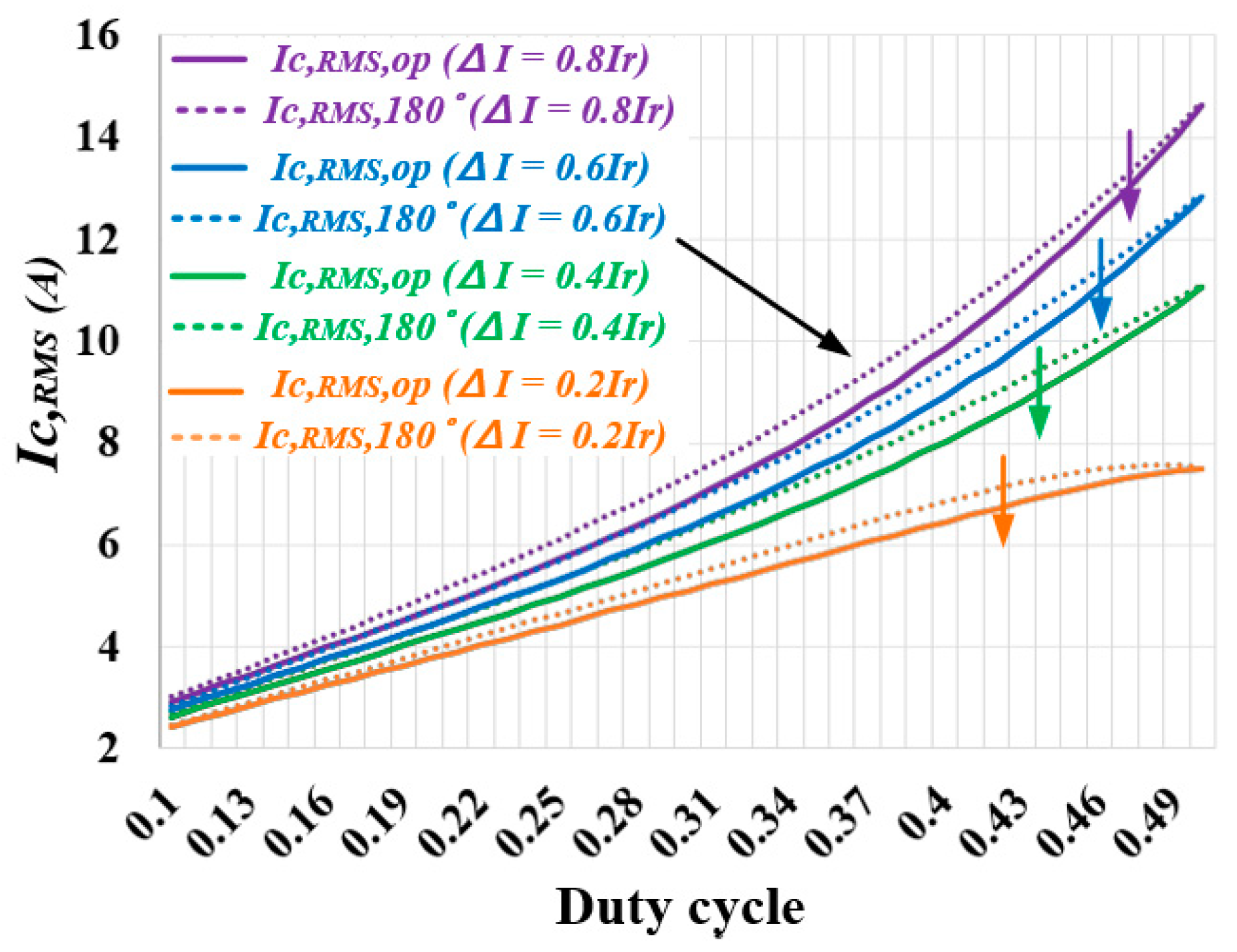
Figure 5 shows the corresponding optimized angle ( Δ θ ) when current variation Δ I is between 0.2 I r and 0.8 I r . As seen in Figure 5, when the duty cycle is <0.5, I C , R M S ( a ) is minimized when a = −0.5 + D 1 . In addition, when Δ I increases, it is evident that Δ θ , which minimizes I C , R M S ( a ) , converges to 180 ° as the duty cycle increases from 0 to 0.5. Here, I C , R M S , o p is the capacitor RMS current when the phase is optimized, and I C , R M S , 180 is the capacitor RMS current when the phase difference between the two legs is 180 ° . Figure 6 shows the change of I C , R M S ( a ) between when the phase difference between the two legs is 180 ° and when the 2-leg interleaved converter’s phase is optimized. The capacitor RMS current decreases when the phase is optimized, as displayed in Figure 6. Simulations and experiments were then conducted to confirm that the proposed phase optimization algorithm decreased the capacitor RMS current.

4. Simulation Results of Proposed Phase Optimization Algorithm

Simulations were conducted based on the phase optimization described in Section 3. Here, a PSIM (PowerSIM) simulator was used to operate the 2-leg conventional interleaved DC–DC converter shown in Figure 1a. Table 1 presents the circuit parameter values of the converter.
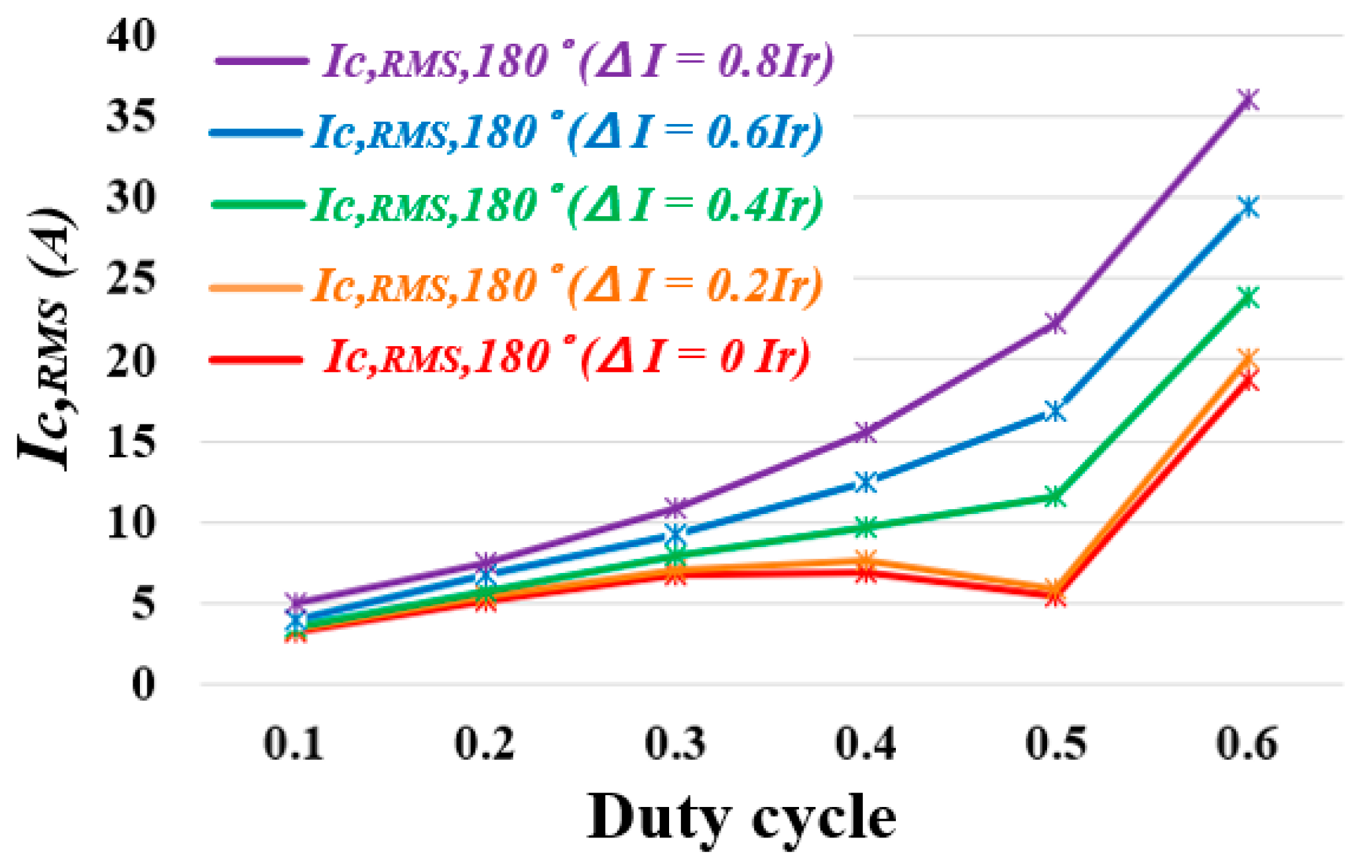
Assuming degradation of the L1-leg of the transistor, the current flowing through the L1-leg was reduced in the simulation. Then, the output capacitor RMS current was compared between when the phase difference of the two legs was 180 ° and when the phase was optimized. Figure 7 shows the capacitor RMS current when the phase difference between the two legs was 180 ° . First, when the duty cycle = 0.1, I C , R M S was increased by 0.09 A ( Δ I = 0.2 I r ) to 1.69 A ( Δ I = 0.8 I r ), and when the duty cycle = 0.2, I C , R M S was increased by 2.11 A ( Δ I = 0.2 I r ) to 4.19 A ( Δ I = 0.8 I r ). Next, when the duty cycle = 0.3, I C , R M S was increased by 3.73 A ( Δ I = 0.2 I r ) to 7.54 A ( Δ I = 0.8 I r ), and when the duty cycle = 0.4, I C , R M S was increased by 4.4 A ( Δ I = 0.2 I r ) to 12.22 A ( Δ I = 0.8 I r ). Additionally, when the duty cycle = 0.5, I C , R M S was increased by 2.53 A ( Δ I = 0.2 I r ) to 18.93 A ( Δ I = 0.8 I r ). The figure shows the same result as presented in Section 3, and it is evident that I C , R M S increased as Δ I increased.
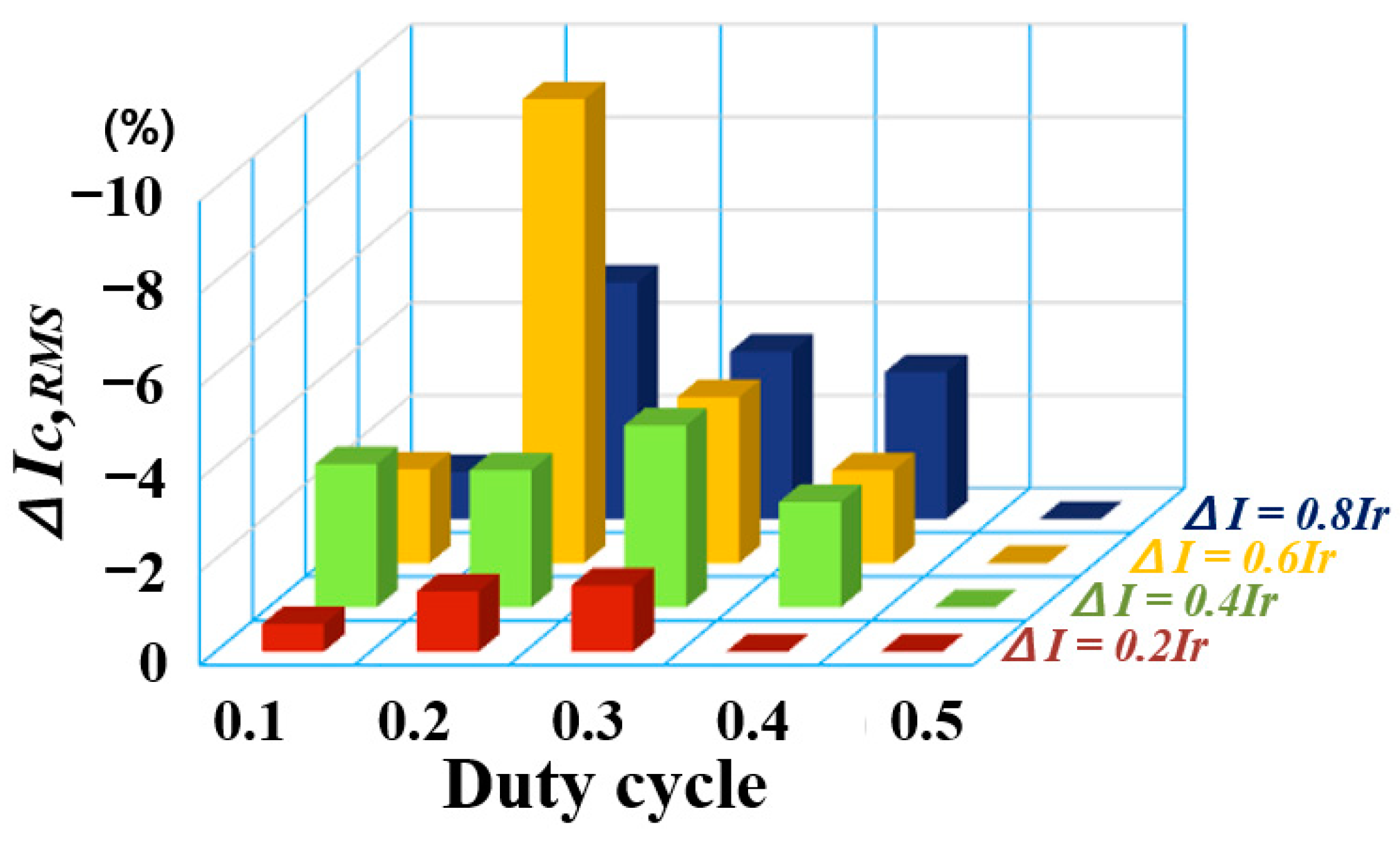
Figure 8 shows the reduction rate of the capacitor RMS current Δ I C , R M S % when the proposed phase optimization algorithm was performed compared to I C , R M S , 180 . This was calculated using Equation (21). As seen in Figure 8, the capacitor RMS current decreased after optimization, which agreed with the result in Section 3. The capacitor RMS current was reduced by up to 10% after applying the phase optimization algorithm, and the reduction rate was 3% to 5% on average.
Δ I C , R M S % = I C , R M S , o p I C , R M S , 180 × 100 I C , R M S , 180 ( % )

5. Experiment Results

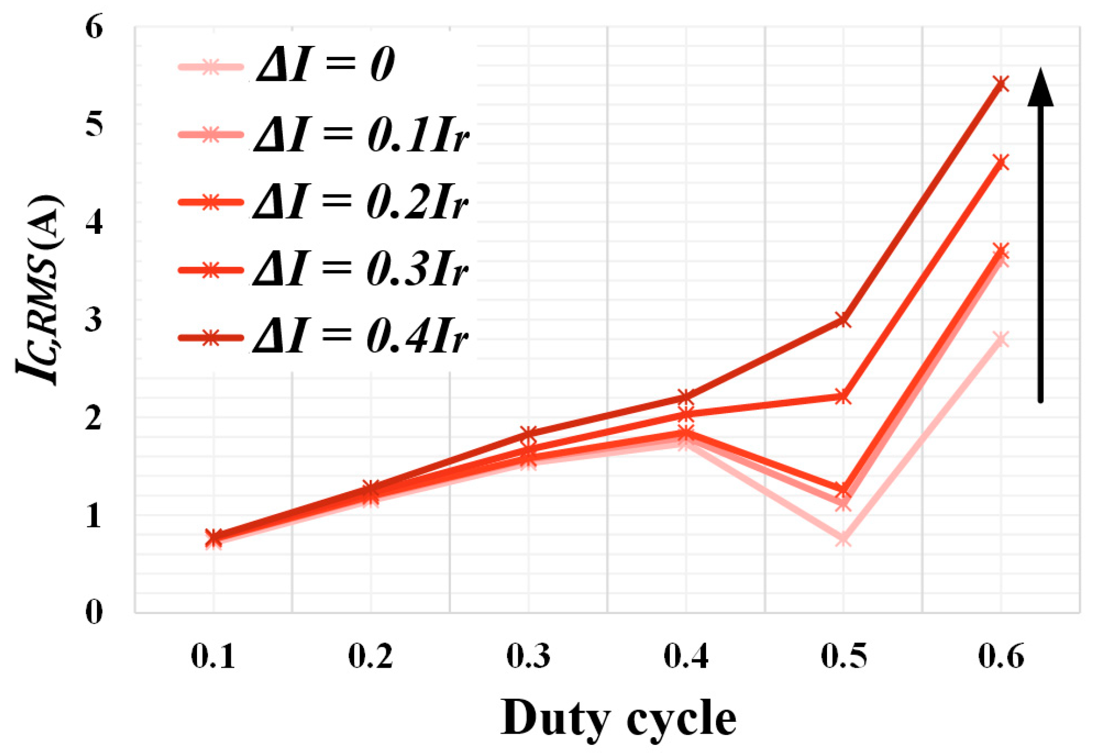
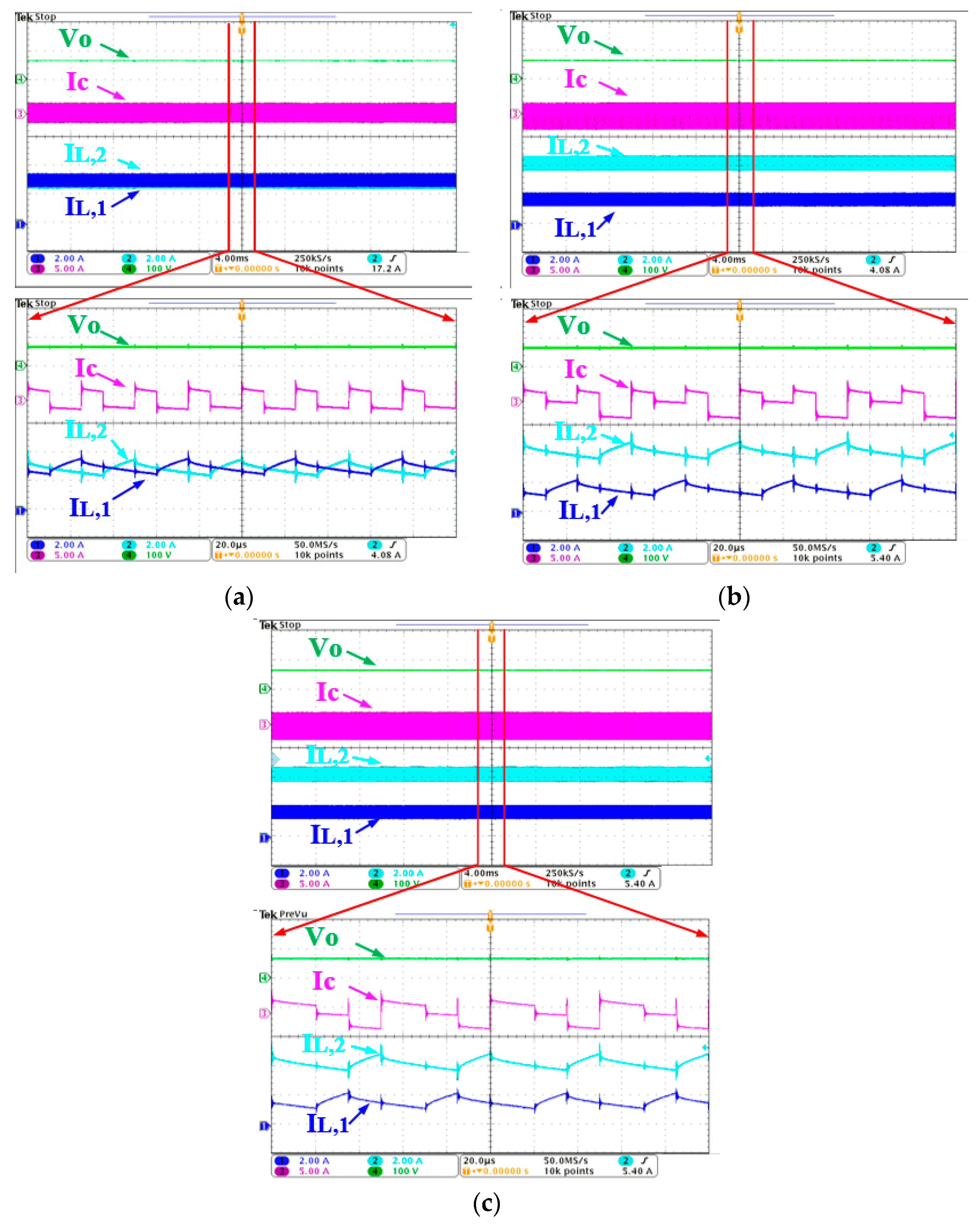
To prove that the proposed 2-leg interleaving DC–DC converter phase optimization algorithm was effective, experiments were conducted following the simulation presented in Section 4 using the converter presented in Figure 1a (as in the simulation). The experimental setup is displayed in Figure 9. The same circuit parameters as those in Table 1 were also used. However, the converter was controlled by applying 48 V as the input voltage. An RSP-1000-48 power supply was used to apply the input voltage. A TMS320F28335 digital signal processor (DSP) was used to control the switching signal. The diodes used in the test were type UJ2D1230K, and the transistors were type SCT3080AL (SiC–MOSFET, V D S S = 650 V, R D S = 80 mΩ, I D S = 30 A) manufactured by ROHM. The capacitor used in the experiment had a rated voltage of 400 V, a capacitance of 680 µF, and an ESR of 366 mΩ (20 °C, 120 Hz). The 2-leg interleaved converter was basically controlled in CCM mode. Next, the output capacitor RMS current was compared between when the phase difference of the two legs was 180 ° and when the phase was optimized. To confirm this, degraded transistors were used in the L1-leg (M1) to decrease its current magnitude. The four types of degraded transistors were labelled A, B, C, and D and were degraded through the HEF experiment. The resistance variations Δ R D S and current variation conditions when using the transistors are displayed in Table 2. Δ R D S of degraded transistor A was 0.107 Ω. When using A, Δ I was 0.1 I r . Δ R D S of degraded transistor B was 0.154 Ω. When using B, Δ I was 0.2 I r . Δ R D S of degraded transistor C was 0.523 Ω. When using C, Δ I was 0.3 I r . Δ R D S of degraded transistor D was 1.23 Ω. When using D, Δ I was 0.4 I r . Subsequently, the changes in capacitor RMS current according to current variations were analyzed. Figure 10 shows the experimental results, which indicated a change in I C , R M S , 180 according to the increase in Δ I . The experiment was conducted while changing Δ I from 0.1 I r to 0.4 I r . As a result, the I C , R M S values increased as Δ I increased, similar to the results from Section 3 and Section 4. In addition, it was evident that the larger the duty cycle, the larger the increase in I C , R M S . Then, to reduce the increased capacitor RMS current, the phase optimization algorithm was applied. Figure 11 shows the experimental results before and after phase optimization. When the duty cycle was 0.3, the output voltage, capacitor current, and each inductor current were measured. Figure 11a demonstrates that the inductor current magnitudes of each leg were the same when the converter’s transistors were not degraded. Figure 11b presents the waveform when the transistor of the L1-leg was degraded. As seen in Figure 11b, the current magnitude of the L1-leg was decreased, while Figure 11c presents the waveform when phase optimization was performed. As seen in Figure 11a–c, it is evident that the output voltage and inductor current were equally controlled. Moreover, there were differences in the capacitor current waveforms. Referring to these differences, the capacitor RMS current was calculated, and the differences were analyzed.
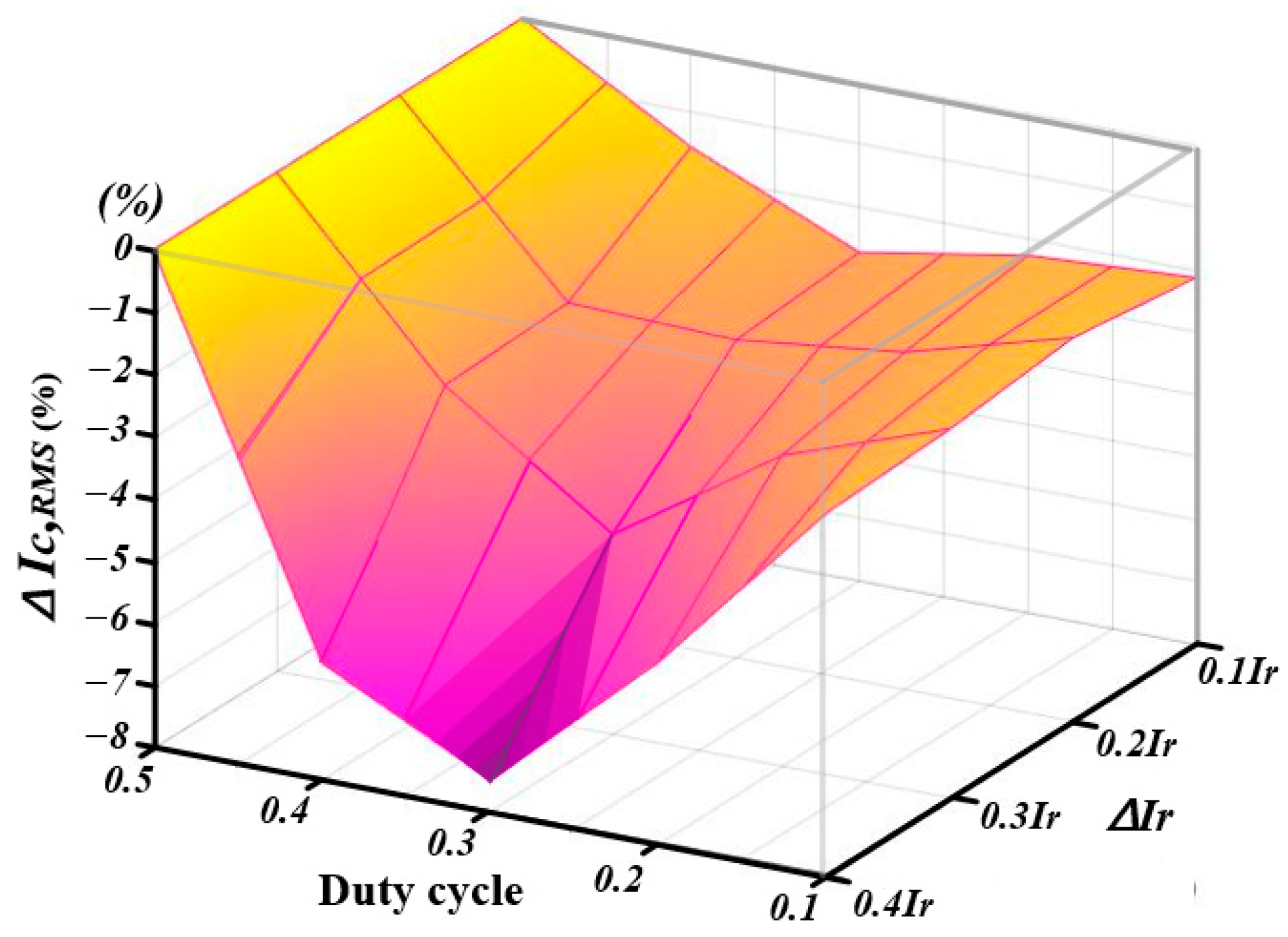
Figure 12 presents the experimental results that display the change in capacitor RMS current before and after phase optimization. The experiment was conducted while changing the current variation Δ I from 0.1 I r to 0.4 I r . Moreover, Δ I C , R M S ( % ) was calculated using Equation (21), and the experimental results according to the variation of Δ I and duty cycle were analyzed. As seen in Figure 12, it is evident that I C , R M S decreased when using the proposed phase optimization algorithm when the phase of each leg was optimized. When the duty cycle was less than 0.4, experiments were conducted to measure I C , R M S . First, when Δ I was 0.1 I r , Δ I C , R M S ( % ) was −0.77% to −2.73%, and when Δ I was 0.2 I r , Δ I C , R M S ( % ) was −1.4% to −2.9%. Next, when Δ I was 0.3 I r , Δ I C , R M S ( % ) was −1.45% to −4.78%, and when Δ I was 0.4 I r , Δ I C , R M S ( % ) was −2.18% to −7.49%. In particular, I C , R M S decreased up to 7.49% after applying the proposed phase optimization algorithm when the duty cycle was 0.3 and Δ I was 0.4 I r . Moreover, since capacitor power loss is proportional to the square of I C , R M S , this was reduced by 14%. In addition, it is evident that the larger the value of Δ I , the larger the reduction rate of Δ I C , R M S ( % ) . If the degree of degradation imbalance of the transistors increased and Δ I was large, the proposed phase optimization algorithm contributed more to improving capacitor efficiency.

6. Conclusions

In 2-leg interleaved DC–DC boost converters, the current magnitude difference of each leg can be increased due to the degradation of the imbalance between transistors. However, this increases the output capacitor RMS current and accelerates the degradation of the capacitor. Through mathematical analysis, simulations, and experiments, the increase of capacitor RMS current was confirmed. In this paper, a phase optimization algorithm was proposed to reduce the increased capacitor RMS current. Next, the phase value at which the capacitor RMS current was minimal was derived through mathematical analysis. Subsequently, simulations and experiments were conducted to apply the phase optimization algorithm. As a result, it was confirmed that the capacitor RMS current decreased when phase optimization was applied. In addition, it was revealed that the reduction rate of the capacitor RMS current was higher when the degradation imbalance of the transistors in each leg was larger.

Author Contributions

Conceptualization: S.K. and S.C.; methodology: S.K. and S.C.; software: J.J.; validation: J.J.; formal analysis: J.J.; investigation: J.J.; resources: S.K.: data curation: J.J.; writing (original draft preparation): J.J.; writing (review and editing): S.K. and S.C.; visualization: J.J.; supervision: S.K.; project administration: S.K.; and funding acquisition: S.K. All authors have read and agreed to the published version of the manuscript.

Funding

This work was supported by a National Research Foundation of Korea (NRF) grant funded by the Korea government (MSIT) (2020R1A2C1013413) and the Korea Electric Power Corporation (Grant number: R21XO01-3).

Data Availability Statement

Not applicable.

Conflicts of Interest

The authors declare no conflict of interest.

References

  1. Ravi, D.; Letha, S.S.; Samuel, P.; Reddy, B.M. An Overview of Various DC-DC Converter Techniques used for Fuel Cell based Applications. In Proceedings of the 2018 International Conference on Power Energy, Environment and Intelligent Control (PEEIC), Greater Noida, India, 13–14 April 2018; pp. 16–21. [Google Scholar]
  2. Syah, M.N.; Firmansyah, E.; Utomo, D.R. Interleaved Bidirectional DC-DC Converter Operation Strategies and Problem Challenges: An Overview. In Proceedings of the 2022 IEEE International Conference in Power Engineering Application (ICPEA), Shah Alam, Malaysia, 7–8 March 2022; pp. 1–6. [Google Scholar]
  3. Aranda, E.D.; Litrán, S.P.; Prieto, M.B.F. Combination of interleaved single-input multiple-output DC-DC converters. CSEE Power Energy Syst. 2022, 8, 132–142. [Google Scholar]
  4. Rahimpour, S.; Tarzamni, H.; Kurdkandi, N.V.; Husev, O.; Vinnikov, D.; Tahami, F. An Overview of Lifetime Management of Power Electronic Converters. IEEE Access 2022, 10, 109688–109711. [Google Scholar] [CrossRef]
  5. Chakraborty, S.; Hasan, M.M.; Paul, M.; Tran, D.; Geury, T.; Davari, P.; Blaabjerg, F.; Baghdadi, M.E.; Hegazy, O. Real-Life Mission Profile-Oriented Lifetime Estimation of a SiC Interleaved Bidirectional HV DC/DC Converter for Electric Vehicle Drivetrains. IEEE Emerg. Sel. Topics Power Electron. 2022, 10, 5142–5167. [Google Scholar] [CrossRef]
  6. Givi, H.; Farjah, E.; Ghanbari, T. A Comprehensive Monitoring System for Online Fault Diagnosis and Aging Detection of Non-Isolated DC–DC Converters’ Components. IEEE Trans. Power Electron. 2019, 34, 6858–6875. [Google Scholar] [CrossRef]
  7. Khosroshahi, A.; Abapour, M.; Sabahi, M. Reliability Evaluation of Conventional and Interleaved DC–DC Boost Converters. IEEE Trans. Power Electron. 2015, 30, 5821–5828. [Google Scholar] [CrossRef]
  8. Yang, S.; Bryant, A.; Mawby, P.; Xiang, D.; Ran, L.; Tavner, P. An Industry-Based Survey of Reliability in Power Electronic Converters. IEEE Trans. Ind. Appl. 2011, 47, 1441–1451. [Google Scholar] [CrossRef]
  9. Song, Y.; Wang, B. Quantitative evaluation for reliability of hybrid electric vehicle powertrain. In Proceedings of the 4th International Conference on Power Engineering, Energy and Electrical Drives, Istanbul, Turkey, 13–17 May 2013; pp. 1404–1409. [Google Scholar]
  10. Murken, M.; Gratzfeld, P. Reliability Comparison of Bidirectional Automotive DC/DC Converters. In Proceedings of the 2017 IEEE 86th Vehicular Technology Conference (VTC-Fall), Toronto, ON, Canada, 24–27 September 2017; pp. 1–7. [Google Scholar]
  11. Ni, Z.; Lyu, X.; Yadav, O.P.; Singh, B.N.; Zheng, S.; Cao, D. Overview of Real-Time Lifetime Prediction and Extension for SiC Power Converters. IEEE Trans. Power Electron. 2020, 35, 7765–7794. [Google Scholar] [CrossRef]
  12. Hannonen, J.; Honkanen, J.; Ström, J.-P.; Kärkkäinen, T.; Silventoinen, P.; Räisänen, S. Capacitor aging detection in DC-DC converter output stage. In Proceedings of the 2015 IEEE Energy Conversion Congress and Exposition, Montreal, QC, Canada, 20–24 September 2015; pp. 5538–5545. [Google Scholar]
  13. Laadjal, K.; Sahraoui, M.; Cardoso, A.J.M. On-Line Fault Diagnosis of DC-Link Electrolytic Capacitors in Boost Converters Using the STFT Technique. IEEE Trans. Power Electron. 2021, 36, 6303–6312. [Google Scholar] [CrossRef]
  14. Wang, H.; Blaabjerg, F. Reliability of Capacitors for DC-Link Applications in Power Electronic Converters—An Overview. IEEE Trans. Ind. Appl. 2014, 50, 3569–3578. [Google Scholar] [CrossRef] [Green Version]
  15. Samavatian, V.; Fotuhi-Firuzabad, M.; Dehghanian, P.; Blaabjerg, F. Reliability Modeling of Multistate Degraded Power Electronic Converters With Simultaneous Exposure to Dependent Competing Failure Processes. IEEE Access 2021, 9, 67096–67108. [Google Scholar] [CrossRef]
  16. Andresen, M.; Buticchi, G.; Liserre, M. Active thermal control of isolated soft switching DC/DC converters. In Proceedings of the IECON 2016—42nd Annual Conference of the IEEE Industrial Electronics Society, Florence, Italy, 23–26 October 2016; pp. 6818–6823. [Google Scholar]
  17. Dusmez, S.; Akin, B. An Active Life Extension Strategy for Thermally Aged Power Switches Based on the Pulse-Width Adjustment Method in Interleaved Converters. IEEE Trans. Power Electron. 2016, 31, 5149–5160. [Google Scholar] [CrossRef]
  18. Marquez, A.; Leon, J.I.; Hahn, F.; Merchan, R.G.; Buticchi, G.; Vazquez, S.; Gerada, C.; Liserre, M.; Franquelo, L.G. Power Devices Aging Equalization of Interleaved DC–DC Boost Converters via Power Routing. IEEE. Emerg. Sel. Topics Ind. Electron. 2020, 1, 91–101. [Google Scholar] [CrossRef]
  19. Karki, U.; Gonzalez-Santini, N.S.; Peng, F.Z. Effect of gate-oxide degradation on electrical parameters of silicon carbide MOSFETs. IEEE Trans. Electron. Devices 2020, 67, 2544–2552. [Google Scholar] [CrossRef]
  20. Jensen, W.R.; Foster, S.N. Online detection of MOSFET gate oxide degradation in a three-phase inverter-drive application. IEEE Trans. Transp. Electrif. 2021, 7, 50–57. [Google Scholar] [CrossRef]
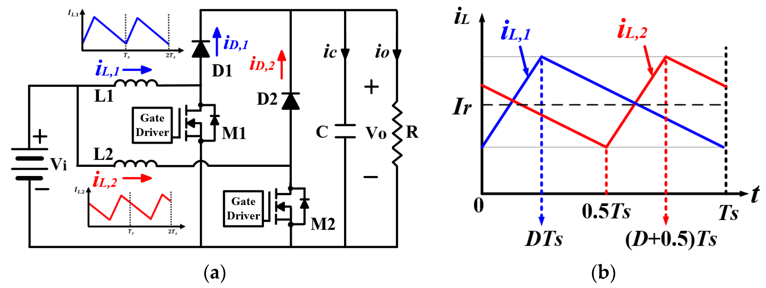
Figure 1. Conventional 2-leg interleaved DC–DC boost converter: (a) circuit diagram; (b) inductor current waveform of each leg.
Machines 11 00624 g001
Figure 2. (a) Inductor current waveform of each leg. (b) Diode current waveform of each leg. (c) Capacitor current waveform by each leg.
Machines 11 00624 g002aMachines 11 00624 g002b
Figure 3. I C , R M S variation according to the amount of inductor current change ( Δ I ).
Machines 11 00624 g003
Figure 4. Capacitor current waveforms with phase shift. (a) at interval (i) −0.5 ≤ a < −0.5 + D 1 , (b) at interval (ii) −0.5 + D 1 a < 0.5 D 2 , (c) at interval (iii) 0.5 D 2 ≤ a < D 1 D 2 + 0.5.
Machines 11 00624 g004
Figure 5. Minimization I C , R M S optimization phase graph.
Machines 11 00624 g005
Figure 6. Variation of I C , R M S before and after phase optimization.
Machines 11 00624 g006
Figure 7. Simulation result: amount of change in I C , R M S , 180 according to increases in Δ I .
Machines 11 00624 g007
Figure 8. Capacitor RMS current reduction rate when applying the proposed phase optimization algorithm in a simulation.
Machines 11 00624 g008
Figure 9. Experiment setup.
Machines 11 00624 g009
Figure 10. I C , R M S , 180 variation according to increases in Δ I .
Machines 11 00624 g010
Figure 11. Interleaving converter experimental waveform with duty cycle of 0.3 (a) when there is no change in current magnitude and phase of each leg, (b) when current in L1-leg decreases, and (c) when phase optimization is performed in (b).
Machines 11 00624 g011
Figure 12. Capacitor RMS current reduction rate when applying the proposed phase optimization algorithm in the experiment.
Machines 11 00624 g012
Table 1. Circuit parameters of the simulation.
Circuit Parameters
L11 mH
L21 mH
Switching Frequency20 kHz
R22 Ω
C680 µF
Vi200 V
Table 2. Experimental conditions depending on SiC-MOSFET degradation.
ABCD
Δ R D S 0.107 Ω0.154 Ω0.523 Ω1.23 Ω
Current   Variation   ( Δ I ) 0.1 I r 0.2 I r 0.3 I r 0.4 I r
Disclaimer/Publisher’s Note: The statements, opinions and data contained in all publications are solely those of the individual author(s) and contributor(s) and not of MDPI and/or the editor(s). MDPI and/or the editor(s) disclaim responsibility for any injury to people or property resulting from any ideas, methods, instructions or products referred to in the content.