Article

Improved Wafer Map Inspection Using Attention Mechanism and Cosine Normalization

1
Faculty of Information Technology, Beijing University of Technology, Beijing 100124, China
2
Beijing Key Laboratory of Computing Intelligence and Intelligent System, Beijing University of Technology, Beijing 100124, China
3
Ministry of Education, Engineering Research Center of Digital Community, Beijing 100124, China
*
Author to whom correspondence should be addressed.
Machines 2022, 10(2), 146; https://doi.org/10.3390/machines10020146
Submission received: 28 December 2021 / Revised: 30 January 2022 / Accepted: 15 February 2022 / Published: 17 February 2022

Abstract

:
Wafer map inspection is essential for semiconductor manufacturing quality control and analysis. The deep convolutional neural network (DCNN) is the most effective algorithm in wafer defect pattern analysis. Traditional DCNNs rely heavily on high quality datasets for training. However, obtaining balanced and sufficient labeled data is difficult in practice. This paper reconsiders the causes of the imbalance and proposes a deep learning method that can learn robust knowledge from an imbalanced dataset using the attention mechanism and cosine normalization. We interpret the dataset imbalance as both a feature and a quantity distribution imbalance. To compensate for feature distribution imbalance, we add an improved convolutional attention module to the DCNN to enhance representation. In particular, a feature-map-specific direction mapping module is developed to amplify the positional information of defect clusters. For quantity distribution imbalance, the cosine normalization algorithm is proposed to replace the fully connected layer, and classifier fine-tuning is realized through a small amount of iterative training, which decreases the sensitivity to the quantitative distribution. The experimental results on real-world datasets demonstrate that the proposed method significantly improves the robustness of wafer map inspection and outperforms existing algorithms when trained on imbalanced datasets.

1. Introduction

Wafers are important carriers for semiconductor manufacturing, and their production process is complex and precise. Wafer production requires a number of processes, such as dissolution of silica sand, purification, crystal drawing, slicing, and cutting. Then, lithography, ion implantation, etching, heat treatment and other operations generate chips (also known as grains) on the wafer. Any fault may result in a product exception. Preceding chip slicing and packaging, the wafer is usually subjected to a probe test, which checks the electrical properties of the grains and then labels the failed grains on a wafer map for technical analysis. Inspection of the wafer map is an important way for improving product yield and evaluating the manufacturing process [1]. When an exception occurs, the defective grains gather in a distribution pattern on the wafer, allowing engineers to trace the cause of the failure based on the type of defect cluster. Common wafer map defect patterns in manufacturing include None, Edge-Ring, Edge-Local, Center, Local, Scratch, Random, Donut and Near-Full patterns, which are included in the public WM-811K [2] real-world dataset. Figure 1 illustrates the examples of typical patterns, each of them reflects specific process failure information. For example, the Center pattern means that the mechanical polishing is uneven, or the pressure of the liquid is abnormal. Abnormal temperature control during annealing may lead to an Edge-Ring pattern. The Scratch pattern indicates an exception in the moving or cutting processes. Note that the None pattern is a normal pattern but still contains defective grains with random distribution. This is caused by cleaning problems in cleaning rooms, which are expensive to eliminate completely; thus, these defective grains are often considered noise.
The current ways of wafer map inspection rely heavily on manual eye inspection. It is necessary to replace this method, which has a high labor cost and low efficiency, with an intelligent fault diagnosis system. Some automatic detection techniques have not been widely used in wafer testing because existing analysis algorithms cannot achieve satisfactory accuracy of defect pattern recognition. Recently, deep learning-based methods have made unprecedented progress, but the related research still remains in the theoretical stage. The main obstacle is that it is difficult to obtain a high-quality dataset for training. The available data obtained in industrial scenarios are usually small and imbalanced, which hinders the application of data-driven deep learning technologies [3].
Previous studies aimed at solving the problem of imbalanced datasets mainly used data augmentation to expand the few shot categories [4,5,6]. This is based on a hypothesis that the model is weak in recognition of categories with few shot samples. However, we found that deep learning model training based on the original dataset may have a high detection accuracy for the few shot categories. In Figure 2, the column graph shows the quantity distribution of labeled wafer maps in the WM-811K dataset (the samples are divided according to the ratio of training set: validation set: test set = 60%:15%:25%). The broken line shows the classification accuracy of ResNet-18 trained with the labeled data. This dataset presents a long-tailed distribution: more header data (categories with large sample sizes) and less tail data (categories with small sample sizes) [7]. It was found that although the sample size of Near-Full pattern was small, the recognition rate was high. While the sample sizes of Edge-Local and Local patterns were large, the recognition rates were very low. According to the defect cluster characteristics, we argue that the features of Near-Full pattern are easy to identify and do not need large-scale sample training, while the features of Edge-Local and Local patterns are difficult to distinguish. We speculate that this is because the difficulty of feature recognition varies between classes. Therefore, it inspired us to define this conjecture as the feature distribution imbalance and include it as one of the perspectives to solve the dataset imbalance.
In this paper, we investigate how to train a deep learning model using an imbalanced dataset to achieve satisfactory defect-pattern-recognition results. Different from the methods based on data augmentation [4,5,6], we argue that the dataset imbalance is not only caused by the quantity imbalance, but also related to the different difficulties of feature recognition between classes, which is called feature distribution imbalance. The proposed method solves the problem of dataset imbalance from both a feature and a quantity distribution imbalance without changing the original dataset. We propose two specific contributions: (1) an improved convolutional block attention module (CBAM) is proposed to enhance the wafer map feature representation of the deep learning model and solve the problem of feature imbalance; (2) a cosine normalization algorithm is proposed to replace the fully connected layers, which can reduce the sensitivity of the classifier to the input data distribution and solve the problem of quantity imbalance. Experiments on the WM-811K dataset showed that both the attention mechanism and the cosine normalization proposed could significantly improve the performance of the deep learning model trained with imbalanced datasets.
The rest of the paper is organized as follows: Section 2 presents a literature review of wafer map defect pattern classification, attention mechanism and long-tailed recognition. Section 3 introduces the specific implementation scheme, including the ResNet backbone, the principle of improved attention mechanism and cosine normalization. Section 4 describes the experimental results, and the last section gives the conclusion.

2. Related Work

2.1. Wafer Map Defect Pattern Classification

Early wafer map defect pattern classification algorithms focused on the feature representation of defect clusters and adopted a two-stage strategy of feature representation and classifier learning. Hwang and Kuo [8] used the principal curve and the binary normal distribution to model defect clusters and identified defect patterns by comparing the logarithmic likelihood probabilities of the two models. Projective features based on the Radon transform and geometric morphological features of defect clusters are commonly used. Wu et al. [2] selected a support vector machine (SVM) as a classifier based on the above features and achieved an average accuracy of 83.1% for the WM-811K dataset. Piao et al. [9] proposed a decision tree ensemble learning scheme that has a good ability to distinguish Center, Donut, Random and None patterns in the WM-811K dataset but has poor recognition capacity for other patterns. Saqlain et al. [10] found that a single classifier could not adapt to complex and varied defect patterns, so they proposed an ensemble learning scheme that extracted multiple feature sets based on geometry, Radon transform and density. They also built an ensemble learning system of logistic regression, random forest, gradient enhancement and artificial neural network, which achieved high accuracy. Clustering methods based on defect characteristics are also widely used, including density-based clustering [11], K-means clustering [12], and hierarchical clustering [13].
Although traditional methods have led to some progress in the field of wafer map defect pattern classification, there are still many problems. On the one hand, feature representation depends too much on manual selection, and feature representation ability markedly affects model performance. On the other hand, classifier selection and parameter tuning are complicated, and the ensemble learning scheme greatly increases the complexity of the model. Recently, deep learning has promoted the upgrading of intelligent manufacturing industry. It has been broadly used in the inspection of solar panels [14], fault diagnosis of bearings [15], detection of unmanned aerial vehicle blade damage [16] and so on. Moreover, it also provides a new solution for wafer map inspection. Unlike the traditional feature engineering, a deep convolutional neural network (DCNN) is an end-to-end scheme with self-learning feature representation and classification abilities, which greatly improve the model’s performance.
Nakazawa et al. [17] took the lead in trying to use convolutional neural networks in the field of wafer map inspection. They used a shallow network to train the simulation dataset and achieved high accuracy with real data. Furthermore, they proposed a defect cluster segmentation method based on a deep learning model [18]. Their works fully verified the feasibility of using DCNNs in the field of wafer map inspection. Park et al. [19] used a Siamese network to learn the feature space of the wafer map and judged specific categories based on Gaussian mean clustering and outlier detection to reduce the uncertainty caused by labeling errors. Ensemble convolutional neural network [20] integrates the main weights of the LeNet, AlexNet and GooleNet classifiers to improve the defect pattern recognition rate of the wafer map and avoid the deficiency of single model representation. There is also some computational cost to this. However, deep learning relies excessively on strict data annotation and sample quality; imbalanced datasets will lead to nonrobust feature representation. Extension methods based on DCNNs have been widely studied. Maksim [4], Saqlain [5] and Wang [6] used synthetic samples (generated by simulation) and data augmentation techniques (randomly rotating, cutting, scaling, etc.) to expand the dataset of few shot categories, which effectively suppressed the poor generalization and overfitting problems of the deep learning model. DenseNet-based transfer learning (T-DenseNet) uses pretrained weights to quickly generalize without requiring excessive data [21]. These methods only solve the problem of imbalanced datasets from the perspective of quantity distribution and ignore the problem of large interclass similarity. Our work will address the problem of dataset imbalance from both feature and quantity distribution perspectives.

2.2. Attention Mechanism

When people observe an object, they tend to quickly scan the global image and then focus on the key areas to suppress unimportant information, which is the mechanism of visual attention [22]. The attentional mechanism can help the DCNNs to mine the important features of the undistinguishable wafer maps to increase the discrimination of interclass features. The spatial transformer layer proposed by Max et al. [23] has strong shift, rotation and scaling invariance, which can transform the original spatial information into a new space and retain the critical feature information. Coordinate attention aims to mine the relative positional information of important features [24]. The above methods are spatial domain attention mechanisms. The squeeze-and-excitation network (SENet) mines the important information of channel features by establishing the dependency relationship between channels and amplifies the influence of key features on the model decision [25]. Inspired by the size adaptive adjustment of the receptive field in the visual cortex with external stimuli, Li et al. [26] proposed a selective kernel network (SKNet), which has a similar structure and mode of action as SENet. However, different receptive field sizes, such as 3 × 3, 5 × 5 and 7 × 7, were used to obtain salient features. SENet and SKNet are both channel domain attention mechanisms. The attention mechanism of a single domain tends to lose important information. CBAM [27] is a hybrid domain method that includes two parts: a channel attention module and a spatial attention module, which focus on the “what” and “where” of the extracted features, respectively. CBAM provides a flexible modular combination that can be adapted to a variety of tasks. Although attention mechanism is the hotspot of computer vision, to the best of our knowledge, there is no attempt at attention mechanism in wafer map inspection. Our research is implemented based on the excellent work of CBAM, as wafer map defect pattern classification requires not only accurate defect cluster information but also location information. For example, the only difference between Edge-Local and Local patterns is the position of the defect cluster. Positional information is also critical for identifying Scratch and Edge-Ring patterns. However, the spatial attention part of CBAM does not sufficiently express the positional characteristics of the wafer map. This paper will analyze the reasons and make targeted improvements.

2.3. Long-Tailed Recognition

Dataset imbalance is common in the real world, especially when the data is collected from production lines, as wafers are. Due to the different frequencies of occurrence, the number of categories presents a long-tailed distribution. Long-tailed recognition has been widely studied in the field of computer vision in recent years [28,29]. For imbalanced datasets with long-tailed distributions, the common processing methods include applying sampling strategies [30,31,32], increasing the weight loss of the tail categories [33,34], and migrating prior knowledge of the head categories [35,36]. Recently, research by Kang [31] and Zhou [32] revealed that the feature representation (usually referred to as the convolution layer) of deep learning models and the classifier (fully connected layer) are not coupled. Imbalanced data distribution has a great impact on the classifier. Although resampling and reweighting strategies balance the classifier’s weights, they reduce the learning ability of the model representation. In contrast, using raw data distribution (without any sampling tricks) to train the model facilitates feature representation. Therefore, based on the above studies, we used the original imbalanced wafer dataset to train a good feature representation module and then designed the algorithm fine-tuning classifier module.

3. Proposed Method

In this section, we describe the specific methods for training deep learning models based on imbalanced wafer datasets. The main steps are as follows: (1) we conduct noise reduction on the wafer map to filter out random defective grains. (2) ResNet-18 is chosen as the backbone network. Based on studies by Kang [31] and Zhou [32], we follow the decoupling learning scheme. In the feature representation learning stage, we add the attention mechanism into the network to enhance the feature representation, mine more identifiable features, and solve the problem of imbalanced feature distribution. We focus on how to use the attention mechanism to amplify the influence of defect cluster positional information and propose a feature-map-specific direction mapping module to replace the spatial attention module in CBAM. (3) In the classifier learning stage, we use the cosine normalization to replace the fully connected layer and fine-tune the weight of the classifier through a small number of iterative fine-tuning to solve the problem of quantity imbalance.

3.1. Wafer Map Processing

Random defective grains are caused by environmental factors in the cleaning room and are expensive to eliminate completely. A large number of studies have proven that the denoising of a wafer map can significantly improve model performance. The constrained mean filtering (C-mean filtering) [37] is an improved mean filtering algorithm that filters only the defective grains and prevents the edge and normal grains from being destroyed. Different from other filtering methods, C-mean filtering only deals with the neighborhood of defective grains. The mean value of pixels are calculated in the filter first. If the mean value is less than the preset threshold, the target defective grain will be converted to normal grain, otherwise it will remain unchanged. Figure 3 shows the filtering results with a 3 × 3 filtering window and a mean threshold of 1.25. It can be seen from the figure that C-mean filtering can effectively filter out irrelevant random noises. The samples used in the following training and testing are all preprocessed by noise reduction.

3.2. ResNet Backbone

In the field of computer vision, many excellent DCNN architectures have been proposed and applied to image classification tasks. We chose ResNet [38] as the backbone for the classification of wafer map defect patterns.
It is well known that deep networks can improve the expression ability of models, but they easily cause gradient disappearance or gradient explosion. While the wafer map has little semantic information, texture information is very important, and shallow features are easily lost in deep structures. ResNet is an effective solution for these problems. Residual learning is the core of ResNet, the schematic diagram of a residual unit is shown in Figure 4. The input vector is defined as x , the output is defined as y , and F x is the residual function. Thus, the output of the residual unit can be expressed as:
y = F x + x
The key point of the residual unit is to learn the residual function F x . When F x = 0 , the network output is the identity mapping. However, in the actual learning process, this situation does not exist. Therefore, the residual function of the model will learn new features and have better performance. There is no shortcut connection x in the traditional CNN model, and its introduction will also enhance the expression of shallow features and prevent them from being forgotten in the deep network.
ResNet offers flexible hierarchical selection. Because of the simplicity of the wafer map, we chose the lightweight ResNet-18 as the backbone. Figure 5 shows the detailed network structure and parameters. Take the first convolutional layer as an example to illustrate the meaning of the parameters in the figure: it uses a 7 × 7 convolution kernel, has a step size s equal to 2 × 2, and has 64 output channels. ResNet-18 contains 8 residual units, each consisting of two 3 × 3 convolutional layers. Due to the dimension variation in the output channel, the shortcut connection represented by the black dotted arrow needs to be expanded through a 1 × 1 convolution. Finally, the fully connected layer composed of 9 neurons was connected. To accelerate model convergence and prevent gradient dispersion, a batch normalization operation is added after each convolution layer, and ReLU is used as the activation function.
As mentioned above, the deep learning model training for the imbalanced dataset can be decoupled into two stages of feature representation learning and classifier learning. Decoupling learning is helpful in improving model performance. In ResNet-18, the fully connected layer is the classifier module, and the previous convolution layers construct the feature representation module.

3.3. Enhance Feature Representation

As shown in Figure 2, although the number of Near-Full patterns is small, the recognition accuracy is very high. In contrast, Edge-Local and Local patterns have a large number of samples but low accuracy. This is because of the large interclass similarity difference and the uneven distribution of features. The attention mechanism in computer vision can amplify the influence of the key features so that the model can suppress irrelevant information and enhance feature representation. Many image classification tasks tend to only focus on the “what” of the target, such as cat, dog or car classification, which can extract key features through the channel domain of DCNNs. For wafer map inspection, it is necessary to pay attention to not only the “what” of the defect cluster (geometric features such as area, length, shape, etc.) but also to the “where” of the defect cluster (absolute position on wafer map). Therefore, we chose the hybrid domain CBAM algorithm to enhance the feature learning ability of ResNet.

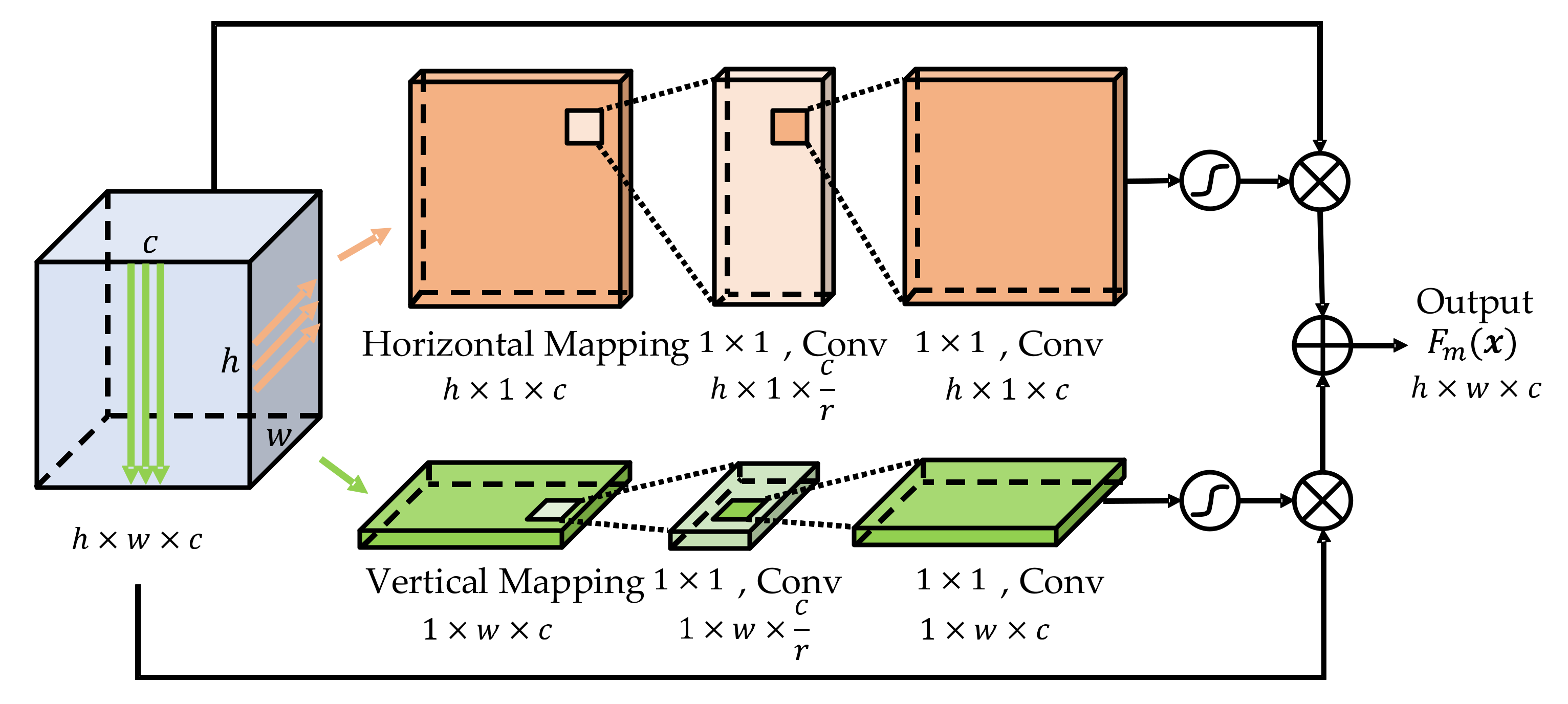
3.3.1. Revisiting The CBAM

CBAM provides attention information in the channel domain and spatial domain of the network. Correspondingly, it is composed of a channel attention module and a spatial attention module. As shown in Figure 6, the two modules are connected in series. x represents the output feature map of any convolution layer, and y represents the output result of the attention operation.
Channel attention module. The channel attention module structure of CBAM is shown in Figure 7. The input feature map x represents the output result of the previous convolution layer. The global average pooling and global maximum pooling operations are carried out on x to obtain the global information of each feature map. Then, they are input into the shared multilayer perceptron (MLP) to enhance the nonlinear expression. The MLP has only one hidden layer, only the output of the hidden layer is activated by ReLU. The output is added by elements to form a 1 × 1 × c vector, which is then mapped to the interval of (0, 1) by the sigmoid function. Finally, the mapping vector is multiplied by the input feature map. The mathematical description of channel attention is shown in (2), where δ represents the sigmoid activation function and F c is the result of the attention mechanism.
F c x = δ M L P M a x P o o l x + M L P A v g P o o l x · x ·
The feature map simulates the characteristics of the visual path. As the feature map of each channel contains different feature descriptions of the input image, there is redundant information. Thus, channel attention amplifies the contribution of useful feature maps and inhibits the influence of irrelevant feature maps, making the model more focused on the “what” of the target.
Spatial attention module. Spatial attention aims to extract the positional information of important objects, i.e., it describes “where” to focus on. The spatial attention module of CBAM is shown in Figure 8. The global maximum pooling and average pooling of the input feature map are performed in the channel dimension, and the concatenation is performed in the channel dimension. This operation aggregates the feature information of all channels. A 7 × 7 convolution kernel is used to extract spatial features. The spatial attention module can be described by (3), where C o n v C A × B represents the convolution operation with the kernel size of A × B and the number of output channels C, and ·   ;   · represents the feature maps concatenating operation.
F s x = δ C o n v 1 7 × 7 M a x P o o l x ; A v g P o o l x · x ·

3.3.2. Improved CBAM

For wafer map inspection, it is necessary to identify not only the geometric characteristics of defect clusters (for example, a large area of defects may form a Random or Near-Full pattern, and a strip of defects may be Edge-Ring or Scratch patterned), but also the positional information (for example, Edge-Local differs only from the Local pattern in that the distribution location is different; the Donut pattern is distributed around the center, and the location is also critical to identify the Edge-Ring and Scratch patterns). In this paper, it is considered that the imbalance of feature distribution in the WM-811K dataset is caused by different interclass similarities. Improving the expression of geometric features and positional information in a deep learning model can effectively mine the features of hard samples. Therefore, we implement it, based on a CBAM algorithm. However, we noticed that the original CBAM did not significantly improve the recognition accuracies of Local and Edge-Local patterns. We judged that the spatial attention module of CBAM fails to capture the key position information of the wafer map. Therefore, although we used the channel attention module in the original CBAM, we needed to rethink and design the spatial attention module.
Feature-map-specific direction mapping module. The spatial attention module in the original CBAM aggregates the information of all channels through global pooling (changing the channel dimension from c dimensions to 1 dimension). However, it should be noted that the feature map of each channel expresses different meanings, and such simple aggregation destroys the feature representation of each channel. To solve this problem, we propose a feature-map-specific direction mapping module. The detailed structure is shown in Figure 9.
For the input feature map x , we reserved the channel dimension and conducted one-dimensional pooling operations for each feature map in the horizontal (along the w axis) and vertical (along the h axis) directions, as shown in (4) and (5):
f H x c = 1 w i = 1 w x c i
f V x c = 1 h j = 1 h x c j
where x c represents the feature map vector of the c-dimensional channel in the input feature map and w and h represent the width and height of the feature map, respectively. This operation obtains aggregate information in the width and height directions. The compression and extension operations capture the dependencies among channels [25,27]. As shown in Figure 9, we used convolution to compress and expand the channel dimension. A 1 × 1 convolutional operation was used to compress the aggregation features f H x c and f V x c to c/r in the channel dimension and then extend them to the c dimension. r is the reduction rate. The output is then activated by the sigmoid function (note that only the first convolution requires ReLU activation) and multiplied by the original input to obtain the key features in both the horizontal and vertical directions. The final output is the sum of the horizontal and vertical attention outputs. The above operations can be described by
F m x = δ ( C o n v c 1 × 1 R e L U C o n v c / r 1 × 1 f H x c ) · x + δ ( C o n v c 1 × 1 R e L U C o n v c / r 1 × 1 f V x c ) · x
The main difference between the feature-map-specific direction mapping module and the spatial attention module in the original CBAM is that the former retains the channel dimension and aims to extract the positional information of each feature map, while the latter aggregates all the channels into a single channel. In this implementation, we retain the channel attention module in the original CBAM for mining the geometric features of wafer map defect clusters, replace the spatial attention module with the feature-map-specific direction mapping module, and still adopt the series mode as shown in Figure 6. The improved CBAM algorithm is integrated into the residual unit in the ResNet-18 backbone, and the loading location is shown in Figure 10. During model training, the original dataset and cross entropy loss function are adopted without a sampling strategy so that a better feature representation can be obtained.

3.4. Cosine Normalization

Another factor leading to the imbalance of the wafer map dataset is the quantity distribution imbalance. As shown in the bar chart in Figure 2, 9 species presented a long-tailed distribution. Models based on training from quantity imbalance datasets tend to have poor generalization ability for tail data because quantity imbalance mainly affects the weight distribution of classifiers (ResNet’s fully connected layer) [31,32]. Figure 11 shows the weight distribution of the fully connected layer of ResNet-18. This model was obtained by using the data distribution in Figure 2 and cross-entropy loss training. The decision is biased because the weight of the tail category is significantly lower than that of the head category. The calculation of the fully connected layer of the traditional DCNN is shown in
f x = w · x + b
Since the offset b is often small, the decision result mainly depends on the dot product of the weights with the output vector. It is worth noting that in our ResNet-18, the activation function of the fully connected layer is ReLU, and the decision value is between [0, +∞]. Therefore, the dot product is unbounded and prone to extreme values. To limit the dot product boundary and reduce the variance, we use the cosine normalization to replace the fully connected layer. The calculation of the cosine normalization algorithm is shown in (8), which calculates the angle θ between the weight vector ω and the input vector x. The output value is between [−1, 1], which effectively avoids the problem of extreme values in the weight distribution. During implementation, the fully connected layer needs to be replaced, but its weight ω should be retained. The feature representation (convolution layer) is fixed, and the classifier is fine-tuned with a few iterations over the original dataset. Unlike dataset balancing strategies such as resampling and reweighting, our method does not need to change the original data distribution by manually designing the balancing strategy.
f x = cos θ = w · x w x

4. Experiments and Results

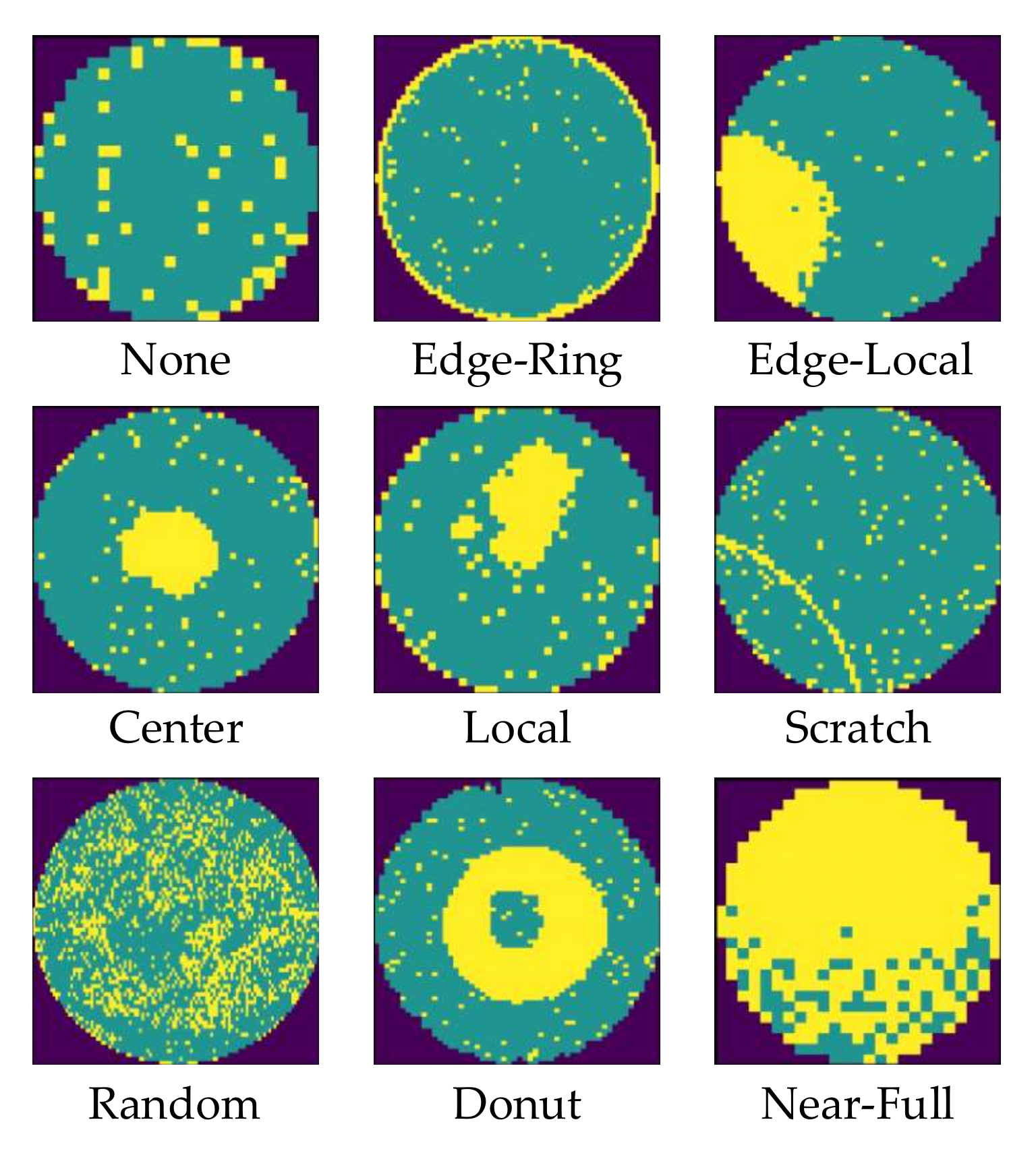
4.1. WM-811K Dataset

This paper uses the WM-811K wafer dataset for training and testing, which is the largest publicly available wafer map dataset to date. The dataset is derived from the real production process of wafers and contains a total of 811,457 samples with 9 defect patterns; only approximately 21% of the samples are labeled. Our experiment is based on labeled samples. Figure 2 shows the detailed data distribution and dataset partitioning. It should be noted that only 10,000 samples of None pattern were selected for the experiment due to the large number of samples. Training and testing of the model were carried out on a DELL T7920 workstation (Round Rock, Texas, USA). The main hardware configuration was two GeForce RTX 2080TI graphics cards and a 64 GB memory. The software environment is Ubuntu 18.04 and was implemented based on the PyTorch deep learning framework. The cross-entropy loss was used for model training, and the initial learning rate was set at 0.01, which was reduced by a factor of ten when the number of iterations reached half of the total number. In the representation learning stage, ResNet-18 integrated with the improved CBAM algorithm was trained for 100 epochs. In the classifier fine-tuning stage, the model based on the previous stage was fine-tuned for 25 epochs at a learning rate of 0.001.

4.2. Selection of Reduction Rate

One of the important operations in the feature-map-specific direction mapping module proposed in this paper is to compress and expand the feature map in the channel dimension and to mine the dependency relationship between channels. The reduction rate r needs to be determined experimentally. We tested the model performance with different values of r on the validation set, as shown in Table 1. The precision, recall rate and F1-score were selected as evaluation criteria. The F1-score is the harmonic mean of precision and recall, which can comprehensively evaluate the model performance. Compared with uncompressed (r = 1) feature maps, compression and expansion can mine the dependencies between channels and improve the performance of the model. When the reduction rate is 16, the model classification effect is optimized; this value was selected in subsequent experiments.

4.3. The Effect of Improved CBAM

To verify the effectiveness of the proposed algorithm, the model classification effects were tested on the test set. The classification confusion matrix is shown in Figure 12, where C1–C9 correspond to None, Edge-Ring, Edge-Local, Center, Local, Scratch, Random, Donut, and Near-Full patterns. Compared with ResNet backbone, the accuracies of Edge-Local, Scratch, Random and Near-Full patterns were significantly improved after the addition of CBAM (as seen from the matrix ResNet + CBAM). Although CBAM improved the model performance, the improvements of Local and Donut patterns were not satisfactory. Edge-local pattern was still confused with Local pattern; and the Donut pattern was easily misidentified as Center or Local pattern. We speculate that this is because the spatial attention in CBAM aggregates all channels, so it does not capture better positional information.
We improved the spatial attention module of CBAM and proposed a feature-map-specific direction mapping module to amplify the position information. As seen from the matrix (ResNet + Improved CBAM), the recognition rates for both Edge-Local and Local patterns were further improved compared to the original CBAM, and the confusion between them had decreased significantly. The Scratch pattern showed the most significant improvement, 6.73% higher than the CBAM, and none of them were judged to be Edge-Ring pattern. The accuracy of the Donut pattern was also improved, and the confusion between Donut and Local pattern was alleviated. Compared with the ResNet backbone, the accuracies of the Edge-Local, Local, Scratch, Random, Donut and Near-Full patterns were increased by 3.24, 3.56, 9.09, 6.51, 4.35 and 5.56%, respectively. The lifting effect of improved CBAM was significantly better than the original CBAM, which indicates that the feature-map-specific direction mapping module works. It is effective to preserve channel dimensions and calculate the positional information of each feature map separately because this method avoids the loss of feature map information. As shown in Figure 12, the average accuracies of the three models (ResNet, ResNet + CBAM, ResNet + Improved CBAM) for the nine defect patterns were 90.73, 92.57 and 94.22% respectively. However, the proposed method slightly reduced the recognition rate of the Center pattern, we found it easy to identify as Local or Edge-Local pattern, which may require further exploration of the model’s feature and location representation.
To elucidate more clearly the effect of the attention mechanism, we visualized the results based on the gradient-weighted class activation mapping (Grad-Cam++) algorithm [39]. Figure 13 shows the heat map generated for the last convolution layer based on Grad-Cam++. The higher the temperature (e.g., dark red), the greater the effect was, while the lower the temperature (e.g., dark blue), the worse the effect was. With the addition of the improved CBAM, areas of warm color increased in the visualized results, while the original CBAM and ResNet usually suppressed areas outside the defect cluster. This indicates that the improved method fully considers the spatial position relationship between defect clusters and wafers. For the Scratch pattern, the area of defect clusters captured by the improved method was more precise.

4.4. Comparison with other Attention Mechanisms

There are many approaches to attention mechanisms in computer vision, but not all of them are suitable for wafer map pattern classification. We compared the improved method with the original CBAM [27], the classical SENet [25], SKNet [26] and coordinate attention [24] methods. The attention modules were placed as shown in Figure 10. According to Woo’s work [27], a super-parameter reduction ratio of 16 is considered to achieve a good balance between model accuracy and computational complexity, so we followed this setting. The number of paths for SKNet was set to 2, and 3 × 3 and 5 × 5 receptive fields were selected. Table 2 shows the classification accuracies of nine defect patterns. The improved CBAM was better than the other attention mechanisms. While the accuracies of the None, Edge-Ring and Center patterns were slightly inferior to those of the other methods, the difference was slight.

4.5. Classifier Fine-Tuning Based on Cosine Normalization

In this paper, a cosine normalization algorithm is proposed to replace the fully connected layer to fine-tune the weight of the classifier and alleviate the influence of the input imbalanced distribution. This step needs to be implemented on a trained model. The last fully connected layer of ResNet is removed, but the weights are retained, and the cosine similarity between the weight and the previous layer’s output vector is calculated for the decision output. We fixed the convolutional layer and fine-tuned the weight of the classifier; we iterated 25 epochs at a learning rate of 0.001. Table 3 reflects the classification accuracy before and after classifier fine-tuning. The fine-tuning with cosine normalization significantly improved the recognition effect of the tail categories with fewer samples, such as Scratch, Random and Donut patterns. In addition, we found that the improvement caused by processing quantity imbalance was weak compared to processing feature imbalance.

4.6. Comparison with Common Methods for Dealing with Imbalanced Dataset

To demonstrate the effectiveness of the proposed DCNN method based on attention mechanism and cosine normalization, we compared it with common methods for dealing with an imbalanced dataset. The data augmentation-based methods are widely used in wafer map inspection [4,5,6]. We compared two augmentation schemes: (1) flipping, rotation, cropping, scaling and Gaussian blur [5,6] were performed on the training samples with a probability of 0.5, respectively, examples based on image transformation are shown in Figure 14; (2) generating wafer maps according to the characteristics of defect clusters [4], the generated examples are shown in Figure 15. We expanded the sample size of each category in the training set to 6000 and the trained model based on ResNet-18. In addition, we also introduced the class-balanced sampling and loss weighting for comparison. The sampling-based approach set the same sampling probability for each pattern, i.e., the probability that each pattern would be sampled was 1/C (C is the number of categories). The method based on loss weighting added a penalty term 1 α on the basis of cross entropy loss, as shown in (9). Where α i is the ratio of the sample size of category i to the total sample size of the dataset, y is the ground truth of the input, and y ^ indicates the prediction.
L o s s = 1 α i y log y ^     i C
The experimental results are shown in Table 4. Our method has a better effect on improving the recognition accuracies of few shot patterns, and the average accuracy is significantly higher than others. Data augmentation usually requires a change in the original dataset. Some common transformations are ineffective for the enhancement of symmetric wafer maps, and cropping may lose important defect information. The generation-based method requires a complex feature engineering, which greatly increases the difficulty of implementation, and the correctness of the generated defects is difficult to guarantee. A dataset is over-sampled or under-sampled when using class balanced sampling, which may result in samples being underutilized. The method based on loss weighting amplifies the influence of few shot patterns, but it still not good at mining the features of difficult samples. The compared methods only consider the quantity imbalance. In contrast, our method improved the performance of the DCNN model using imbalanced dataset by solving both quantity imbalance and feature imbalance, and it was easier to implement without changing the distribution of the original dataset.

4.7. Comparison with Classical Wafer Map Inspection Algorithms

We compared the proposed method with the models studied on the WM-811K wafer dataset in recent years, including WMFPR [2], DTE-WMFPR [9], WMDPI [10] and T-DenseNet [21]. We compared the recognition rate of each defect pattern and average accuracy, the results are shown in Table 5. It was found that the proposed method achieved satisfactory average performance, with significant improvement on Edge-Local, Center, Scratch and Donut patterns; other patterns were similar to classical algorithms.

5. Conclusions

Wafer map inspection is an important means of fault diagnosis in semiconductor manufacturing. Although the DCNN-based methods greatly improve the results of wafer map defect pattern recognition, the performance of DCNN is usually limited because of training with an imbalanced dataset. The traditional method based on data augmentation can only solve the quantity imbalance, but is unable to solve the problem of the difficulty of feature recognition varying between classes. We reconsidered the causes of the dataset imbalance and reinterpreted it as the feature distribution and quantity distribution imbalance. On the one hand, we use the improved CBAM to enhance the feature representation of the DCNN, mine the features of difficult samples, and solve the problem of feature distribution imbalance. We focused on spatial attention and proposed a feature-map-specific direction mapping module to amplify the effect of defect cluster positional information on the model decision. On the other hand, the cosine normalization method was proposed to replace the fully connected layer to fine-tune the weight of the classifier and alleviate the sensitivity of the distribution of input data. We verified the effectiveness of the proposed method on the imbalanced WM-811K dataset. Compared with the traditional methods based on data augmentation and other ways of balancing the dataset, our method solved the problem of dataset imbalance more effectively. In addition, since there was no need to change the original dataset, our method was easier to implement. Finally, we achieved an average accuracy of 95.46%, significantly better than the recently developed advanced models.
Overcoming the problem of dataset imbalance can promote the application of the algorithm in real manufacturing. Although our approach has made some progress, the recognition of Local patterns is still not ideal. Many of them are misclassified as the Scratch pattern. This prompts us to strengthen the research on the feature representation of defect clusters in the future.

Author Contributions

Conceptualization, Q.X. and N.Y.; methodology, Q.X.; software, Q.X. and F.E.; validation, Q.X. and F.E.; formal analysis, N.Y.; investigation, Q.X. and F.E.; resources, Q.X.; data curation, Q.X.; writing—original draft preparation, Q.X.; writing—review and editing, Q.X. and N.Y.; visualization, Q.X.; supervision, N.Y.; project administration, N.Y.; funding acquisition, N.Y. All authors have read and agreed to the published version of the manuscript.

Funding

This research was jointly funded by Beijing Municipal Education Commission and Beijing Natural Science Foundation (No. KZ202010005004).

Data Availability Statement

Available online: WM811K: http://mirlab.org/dataSet/public/ (accessed on 28 December 2021).

Conflicts of Interest

The authors declare no conflict of interest.

References

  1. Hsu, C.-Y.; Chen, W.-J.; Chien, J.-C. Similarity matching of wafer bin maps for manufacturing intelligence to empower Industry 3.5 for semiconductor manufacturing. Comput. Ind. Eng. 2020, 142, 106358. [Google Scholar] [CrossRef]
  2. Wu, M.-J.; Jang, J.-S.; Chen, J.-L. Wafer map failure pattern recognition and similarity ranking for large-scale data sets. IEEE Trans. Semicond. Manuf. 2015, 28, 1–12. [Google Scholar]
  3. Lei, L.; Sun, S.; Zhang, Y.; Liu, H.; Xu, W. PSIC-Net: Pixel-wise segmentation and image-wise classification network for surface defects. Machines 2021, 9, 221. [Google Scholar] [CrossRef]
  4. Maksim, K.; Kirill, B.; Eduard, Z.; Nikita, G.; Alexander, B.; Arina, L.; Vladislav, S.; Daniil, M.; Nikolay, K. Classification of wafer maps defect based on deep learning methods with small amount of data. In Proceedings of the 2019 International Conference on Engineering and Telecommunication, Dolgoprudny, Russia, 20–21 November 2019. [Google Scholar]
  5. Saqlain, M.; Abbas, Q.; Lee, J.Y. A deep convolutional neural network for wafer defect identification on an imbalanced dataset in semiconductor manufacturing processes. IEEE Trans. Semicond. Manuf. 2020, 33, 436–444. [Google Scholar] [CrossRef]
  6. Wang, R.; Chen, N. Defect pattern recognition on wafers using convolutional neural networks. Qual. Reliab. Eng. Int. 2020, 36, 1245–1257. [Google Scholar] [CrossRef]
  7. Reed, W.J. The Pareto, Zipf and other power laws. Econ. Lett. 2001, 74, 15–19. [Google Scholar] [CrossRef]
  8. Hwang, J.Y.; Kuo, W. Model-based clustering for integrated circuit yield enhancement. Eur. J. Oper. Res. 2007, 178, 143–153. [Google Scholar] [CrossRef]
  9. Piao, M.; Jin, C.H.; Lee, J.Y.; Byun, J.-Y. Decision tree ensemble-based wafer map failure pattern recognition based on radon transform-based features. IEEE Trans. Semicond. Manuf. 2018, 31, 250–257. [Google Scholar] [CrossRef]
  10. Saqlain, M.; Jargalsaikhan, B.; Lee, J.Y. A voting ensemble classifier for wafer map defect patterns identification in semiconductor manufacturing. IEEE Trans. Semicond. Manuf. 2019, 32, 171–182. [Google Scholar] [CrossRef]
  11. Jin, C.H.; Na, H.J.; Piao, M.; Pok, G.; Ryu, K.H. A novel DBSCAN-based defect pattern detection and classification framework for wafer bin map. IEEE Trans. Semicond. Manuf. 2019, 32, 286–292. [Google Scholar] [CrossRef]
  12. Chen, X.; Zhao, C.; Chen, J.; Zhang, D.; Zhu, K.; Su, Y. K-means clustering with morphological filtering for silicon wafer grain defect detection. In Proceedings of the IEEE 4th Information Technology, Networking, Electronic and Automation Control Conference, Chongqing, China, 12–14 June 2020. [Google Scholar]
  13. Lee, S.; Kim, D. Distributed-based hierarchical clustering system for large-scale semiconductor wafers. In Proceedings of the 2018 IEEE International Conference on Industrial Engineering and Engineering Management, Bangkok, Thailand, 16–19 December 2018. [Google Scholar]
  14. Chen, H.; Pang, Y.; Hu, Q.; Liu, K. Solar cell surface defect inspection based on multispectral convolutional neural network. J. Intell. Manuf. 2020, 31, 453–468. [Google Scholar] [CrossRef] [Green Version]
  15. Nguyen, V.-C.; Hoang, D.-T.; Tran, X.-T.; Van, M.; Kang, H.-J. A bearing fault diagnosis method using multi-branch deep neural network. Machines 2021, 9, 345. [Google Scholar] [CrossRef]
  16. Yang, P.; Wen, C.; Geng, H.; Liu, P. Intelligent fault diagnosis method for blade damage of quad-rotor UAV based on stacked pruning sparse denoising autoencoder and convolutional neural network. Machines 2021, 9, 360. [Google Scholar] [CrossRef]
  17. Nakazawa, T.; Kulkarni, D.V. Wafer map defect pattern classification and image retrieval using convolutional neural network. IEEE Trans. Semicond. Manuf. 2018, 31, 309–314. [Google Scholar] [CrossRef]
  18. Nakazawa, T.; Kulkarni, D.V. Anomaly detection and segmentation for wafer defect patterns using deep convolutional encoder-decoder neural network architectures in semiconductor manufacturing. IEEE Trans. Semicond. Manuf. 2019, 32, 250–256. [Google Scholar] [CrossRef]
  19. Park, S.; Jang, J.; Kim, C.O. Discriminative feature learning and cluster-based defect label reconstruction for reducing uncertainty in wafer bin map labels. J. Intell. Manuf. 2021, 32, 251–263. [Google Scholar] [CrossRef]
  20. Hsu, C.-Y.; Chien, J.-C. Ensemble convolutional neural networks with weighted majority for wafer bin map pattern classification. J. Intell. Manuf. 2022, 33, 831–844. [Google Scholar] [CrossRef]
  21. Shen, Z.; Yu, J. Wafer map defect recognition based on deep transfer learning. In Proceedings of the 2019 IEEE International Conference on Industrial Engineering and Engineering Management, Macao, China, 15–18 December 2019. [Google Scholar]
  22. Mnih, V.; Heess, N.; Graves, A.; Kavukcuoglu, K. Recurrent models of visual attention. In Proceedings of the 27th International Conference on Neural Information Processing Systems, Montreal, QC, Canada, 8–13 December 2014. [Google Scholar]
  23. Jaderberg, M.; Simonyan, K.; Zisserman, A.; Kavukcuoglu, K. Spatial transformer networks. In Proceedings of the 28th International Conference on Neural Information Processing Systems, Montreal, QC, Canada, 7–12 December 2015. [Google Scholar]
  24. Hou, Q.; Zhou, D.; Feng, J. Coordinate attention for efficient mobile network design. In Proceedings of the IEEE/CVF Conference on Computer Vision and Pattern Recognition, Nashville, TN, USA, 20–25 June 2021. [Google Scholar]
  25. Hu, J.; Shen, L.; Albanie, S.; Sun, G.; Wu, E. Squeeze-and-excitation networks. IEEE Trans. Pattern Anal. Mach. Intell. 2019, 42, 2011–2023. [Google Scholar] [CrossRef] [PubMed] [Green Version]
  26. Li, X.; Wang, W.; Hu, X.; Yang, J. Selective kernel networks. In Proceedings of the 32nd IEEE/CVF Conference on Computer Vision and Pattern Recognition, Long Beach, CA, USA, 16–20 June 2019. [Google Scholar]
  27. Woo, S.; Park, J.; Lee, J.-Y.; Kweon, I.S. CBAM: Convolutional block attention module. In Proceedings of the European Conference on Computer Vision, Munich, Germany, 8–14 September 2018. [Google Scholar]
  28. Zhang, J.; Liu, L.; Wang, P.; Zhang, J. Exploring the auxiliary learning for long-tailed visual recognition. Neurocomputing 2021, 449, 303–314. [Google Scholar] [CrossRef]
  29. Yin, X.; Yu, X.; Sohn, K.; Liu, X.; Chandraker, M. Feature transfer learning for deep face recognition with under-represented data. In Proceeding of the IEEE/CVF Conference on Computer Vision and Pattern Recognition, Long Beach, CA, USA, 16-20 June 2019. [Google Scholar]
  30. Mahajan, D.; Girshick, R.; Ramanathan, V.; He, K.; Paluri, M.; Li, Y.; Bharambe, A.; van der Maaten, L. Exploring the limits of weakly supervised pretraining. In Proceedings of the European Conference on Computer Vision, Munich, Germany, 8–14 September 2018. [Google Scholar]
  31. Kang, B.; Xie, S.; Rohrbach, M.; Yan, Z.; Gordo, A.; Feng, J.; Kalantidis, Y. Decoupling representation and classifier for long-tailed recognition. In Proceedings of the International Conference on Learning Representation, Addis Ababa, Ethiopia, 26–30 April 2020. [Google Scholar]
  32. Zhou, B.; Cui, Q.; Wei, X.-S.; Chen, Z.-M. BBN: Bilateral-branch network with cumulative learning for long-tailed visual recognition. In Proceedings of the IEEE/CVF Conference on Computer Vision and Pattern Recognition, Seattle, WA, USA, 13–19 June 2020. [Google Scholar]
  33. Cui, Y.; Jia, M.; Lin, T.-Y.; Song, Y.; Belongie, S. Class-balanced loss based on effective number of samples. In Proceedings of the 2019 IEEE/CVF Conference on Computer Vision and Pattern Recognition, Long Beach, CA, USA, 16–20 June 2019. [Google Scholar]
  34. Cao, K.; Wei, C.; Gaidon, A.; Arechiga, N.; Ma, T. Learning imbalanced datasets with label-distribution-aware margin loss. In Proceedings of the 33rd Annual Conference on Neural Information Processing Systems, Vancouver, BC, Canada, 8–14 December 2019. [Google Scholar]
  35. Liu, J.; Sun, Y.; Han, C.; Dou, Z.; Li, W. Deep representation learning on long-tailed data: A learnable embedding augmentation perspective. In Proceedings of the IEEE/CVF Conference on Computer Vision and Pattern Recognition, Seattle, WA, USA, 13–19 June 2020. [Google Scholar]
  36. Liu, Z.; Miao, Z.; Zhan, X.; Wang, J.; Gong, B.; Yu, S.X. Large-scale long-tailed recognition in an open world. In Proceedings of the IEEE Computer Society Conference on Computer Vision and Pattern Recognition, Long Beach, CA, USA, 15–20 June 2019. [Google Scholar]
  37. Yu, N.-G.; Xu, Q.; Wang, H.-L.; Lin, J. Wafer bin map inspection based on DenseNet. J. Cent. South Univ. 2020, 28, 2436–2450. [Google Scholar] [CrossRef]
  38. He, K.; Zhang, X.; Ren, S.; Sun, J. Deep residual learning for image recognition. In Proceedings of the IEEE Conference on Computer Vision and Pattern Recognition, Las Vegas, NV, USA, 27–30 June 2016. [Google Scholar]
  39. Chattopadhay, A.; Sarkar, A.; Howlader, P.; Balasubramanian, V.N. Grad-CAM++: Generalized gradient-based visual explanations for deep convolutional networks. In Proceedings of the 18th IEEE Winter Conference on Applications of Computer Vision, Lake Tahoe, NV, USA, 12–15 March 2018. [Google Scholar]
Figure 1. Typical wafer map defect patterns in the WM-811K dataset.
Machines 10 00146 g001
Figure 2. Distribution of the WM-811K dataset and classification accuracy of ResNet.
Machines 10 00146 g002
Figure 3. Results of C-mean filtering for wafer maps.
Machines 10 00146 g003
Figure 4. Structure of a residual unit.
Machines 10 00146 g004
Figure 5. Structure of ResNet-18.
Machines 10 00146 g005
Figure 6. Structure of CBAM.
Machines 10 00146 g006
Figure 7. Structure of the channel attention module.
Machines 10 00146 g007
Figure 8. Structure of the spatial attention module.
Machines 10 00146 g008
Figure 9. Structure of the feature-map-specific direction mapping module.
Machines 10 00146 g009
Figure 10. Location of the improved CBAM in the residual unit.
Machines 10 00146 g010
Figure 11. L2-norm of the weights.
Machines 10 00146 g011
Figure 12. The classification confusion matrixes on test set(C1: None, C2: Edge-Ring, C3: Edge-Local, C4: Center, C5: Local, C6: Scratch, C7: Random, C8: Donut, C9: Near-Full). (a) Training based on ResNet. (b) Training based on ResNet and the original CBAM attention mechanism. (c) Training based on ResNet and Improved CBAM attention mechanism.
Machines 10 00146 g012
Figure 13. Visualization based on Grad-Cam++.
Machines 10 00146 g013
Figure 14. Augmentation based on image transformation.
Machines 10 00146 g014
Figure 15. Augmentation based on generation.
Machines 10 00146 g015
Table 1. Influence of reduction rate on model.
rPrecisionRecallF1-Score
10.9240.9320.928
80.9230.9370.930
160.9320.9400.936
320.9270.9380.932
Table 2. Classification accuracies when integrating different attention mechanisms (%).
Attention MechanismNoneEdge-RingEdge-LocalCenterLocalScratchRandomDonutNear-FullAverage
Coordinate [24]98.9097.6691.8298.2383.6188.2293.9588.4197.2293.11
SENet [25]99.1098.3090.2898.1384.2986.5393.2889.8610093.31
SKNet [26]99.1297.7491.2898.0483.7285.5293.0288.4197.2292.68
CBAM [27]98.4298.3292.5997.3983.0585.1993.9588.4110093.04
I-CBAM 198.5597.6492.9897.0185.3889.5994.8892.0310094.22
1 Improved CBAM.
Table 3. Classification accuracies before and after classifier fine-tuning (%).
ModelNoneEdge-RingEdge-LocalCenterLocalScratchRandomDonutNear-FullAverage
ResNet-1898.3197.2389.7498.6081.7280.4788.3787.6894.4490.73
I-CBAM 198.5597.6492.9897.0185.3889.5994.8892.0310094.22
I-CBAM + CN 298.4797.6491.9897.5786.7393.696.7496.3810095.46
1 Add improved CBAM on ResNet-18. 2 Add improved CBAM and cosine normalization on ResNet-18.
Table 4. Comparison with other imbalanced dataset processing methods (%).
ModelNoneEdge-RingEdge-LocalCenterLocalScratchRandomDonutNear-FullAverage
T-based 198.7897.5889.5197.7683.2884.5190.792.0310092.68
G-based 298.597.590.4398.2384.7386.5391.1686.9610092.67
CB-based 398.78 97.989.1298.13 83.39 87.88 92.49 89.3 100 93
LW-based 499.02 97.7891.6797.76 83.39 87.88 92.95 87.68 100 93.13
Proposed98.4797.6491.9897.5786.7393.696.7496.3810095.46
1 Data augmentation based on image transformation. 2 Data augmentation based on image generation. 3 Method based on class balanced sampling. 4 Method based on loss weighting.
Table 5. Comparison with classical wafer map defect pattern classification algorithms (%).
ModelNoneEdge-RingEdge-LocalCenterLocalScratchRandomDonutNear-FullAverage
WMFPR [2]95.779.785.184.968.582.479.87497.983.1
DTE-WMFPR [9]10086.883.595.883.58695.892.3N/A90.5
WMDPI [10]97.997.981.892.583.981.495.891.593.390.7
T-DenseNet [21]85.566.881.564.510072.665.591.299.380.8
Proposed98.697.69297.686.793.696.796.410095.5
Publisher’s Note: MDPI stays neutral with regard to jurisdictional claims in published maps and institutional affiliations.

