1. Introduction
Power converters are systems that convert energy from one form (source) to another form (load), with high performance and efficiency. These systems must ensure compliance with electromagnetic interference (EMI) standards [
1] and high reliability [
2,
3,
4,
5].
Most power converters lack redundancy [
2], such that a failure in one component can lead to the system shutdown. Outages resulting from unexpected failures can decrease system security and increase operating costs [
2,
3]. For instance, in electric or hybrid electric vehicles (HEVs), a failure in the electric propulsion system can reduce the fuel economy and, under certain circumstances, may reduce safety [
2,
3].
Power converters can be subdivided into four categories: AC/AC, AC/DC, DC/DC and DC/AC. This paper focuses on DC/DC converters, which are widely used in several critical systems, such as DC micro grids, electric vehicles, data centers, medical equipment, aerospace power systems, and others [
2,
3,
4,
5]. It is important to highlight that a loss of functionality or an unexpected stoppage of these systems can result in a catastrophe.
In order to improve the reliability of DC-DC converters, two solutions can be implemented: the design of redundant systems [
6,
7] and the implementation of an online FDT [
8,
9] during the converter design. In both cases, the proposed tool can be fundamental.
The design of DC-DC converters requires a set of fundamental concepts, such as the identification of component specifications, choosing the best gate drive circuit and the best heat sinks for the power switch, designing inductors, and solving EMI problems, among others. On the other hand, if the system to be developed fits into a critical application, the development of redundant circuits or the implementation of online FDT is another fundamental aspect of the design process.
In the design process, simulation tools play a key role, as they allow the testing of the proposed solution in a very simple and flexible way. Therefore, before developing the experimental prototype, it is important to carry out a set of tests in a computer simulation environment to verify the feasibility of the proposed solution.
One of the most commonly used tools to simulate DC-DC converters is MATLAB/Simulink [
3,
10,
11,
12,
13]. The simplicity in the design of the DC-DC converters and the user-friendly graphical interface makes MATLAB/Simulink very attractive, playing a fundamental role in carrying out research tasks [
3,
10,
11,
12,
13]. However, as MATLAB is a proprietary programming language, its algorithms are proprietary; thus, it is not possible to access its code. This, particularity, can significantly limit the implementation of control methods, as well as the development of fault diagnostic techniques [
14,
15].
A good alternative to MATLAB is the Python programming language [
15,
16,
17]. Despite the fact that it does not allow a model-based design like MATLAB, it has the computational power and tools to simulate DC/DC converters [
15]. On the other hand, Python is an open-source programming language that has several machine learning algorithms that can be very useful in the development of fault diagnostic techniques for DC-DC converters [
8,
18,
19]. It is important to highlight the fact that simulation techniques based on open-source tools are a very recent topic of investigation [
15,
16,
17], and their application in the scope of FDTs has not been studied. This work intends to demonstrate that the simulation techniques mentioned above can evaluate the applicability of FDTs in DC-DC converters without the need to design an experimental prototype.
The proposed tool simulates the DC-DC converter operating in closed loop, and simultaneously implements the FDT in real time. The FDT used in the scope of this paper uses Fast Fourier Transform (FFT), which is a signal processing method that implicitly uses the concepts of symmetry and asymmetry. The proposed simulation tool can be implemented in a high-level open-source programming language oriented to numerical analysis, such as Python, Scilab or Octave.
The programming language used to implement this tool will be Python, and the DC-DC converter under analysis will be a buck converter operating in closed loop, with a type II compensator.
The rest of this paper is organized as follows.
Section 2 describes the implementation of the proposed tool (the first, second and fourth blocks of the code) for a buck converter operating in closed loop.
Section 3 presents the converter design process, and in
Section 4 a comparison is carried out between the proposed tool and LTspice for validation purposes.
Section 5 presents the implementation of the FDT (the third block of code) using the proposed tool and several experimental results. Finally,
Section 6 presents the conclusions.
2. Simulation Closed-Loop Operation
As mentioned in the previous section, the proposed tool will be implemented in Python, which is a high-level, general-purpose programming language. Therefore, at first it is essential to make the development environment suitable for simulating DC-DC converters.
Python has a vast set of libraries, the most important, in this context, are Numpy and Matplotlib. The Numerical Python package (Numpy) is used for manipulating arrays and matrices, and the Matplotlib package is used for plotting. These libraries make the development environment suitable for numerical analysis.
In the following, it will be described how the proposed tool can be implemented in Python. For this purpose, it will be necessary to divide the code into four modules:
The first module will be responsible for modelling the different states of the converter.
The second module generates a saw-tooth signal that is fundamental for the control section.
The third module implements the FDT, and it will be described in
Section 5.
The fourth module represents the main function, which integrates all of the modules and implements the control section.
2.1. First Module
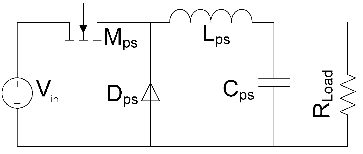
Figure 1 shows an electrical schematic of a buck converter.
During the conduction state, the transistor, Mps, conducts in contrast to the diode, Dps. Consequently, current will flow through the inductor, Lps, which stores energy in the form of a magnetic field; simultaneously, the capacitor, Cps, is charged.
During the non-conduction state, Mps is turned off, which forces the current to freewheel around the path consisting of Lps, Cps and Dps.
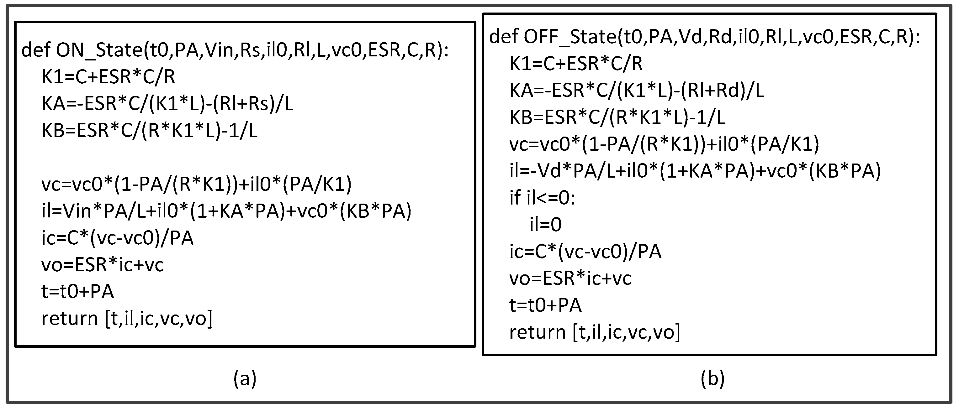
After analyzing the equivalent circuits corresponding to each of the states, equations must be discretized and represented in the form of a function (
Figure 2). This procedure can be found in detail in [
15].
The functions represented in
Figure 2 have the following elements as input arguments: the input voltage (V
in), L
ps resistance (R
L), L
ps inductance (L), M
ps drain-source resistance (R
S), D
ps forward voltage drop (V
d), D
ps internal resistance (R
d), C
ps capacitance (C), C
ps internal resistance (ESR), load resistance (R
Load), initial time (t
0), sample period (PA), L
ps initial condition (i
l0), and C
ps initial condition (v
c0).
The functions represented in
Figure 2 return the following elements: the inductor current (i
L), capacitor current (i
C), output voltage (v
O), output voltage component due exclusively to C (v
C), and time (t), respectively.
The control system designed for the converter assumes that it operates in Continuous Conduction Mode (CCM). However, for short periods of time, namely during the transient regime, the converter might operate in Discontinuous Conduction Mode (DCM). In DCM, the inductor current will be canceled because it cannot reverse polarity due to D
ps. This situation was taken into account in the code, as can be seen in
Figure 2b.
2.2. Second Module
After creating the first module, it is necessary to create the second one, which is essential for the generation of the Pulse Width Modulator (PWM) signal.
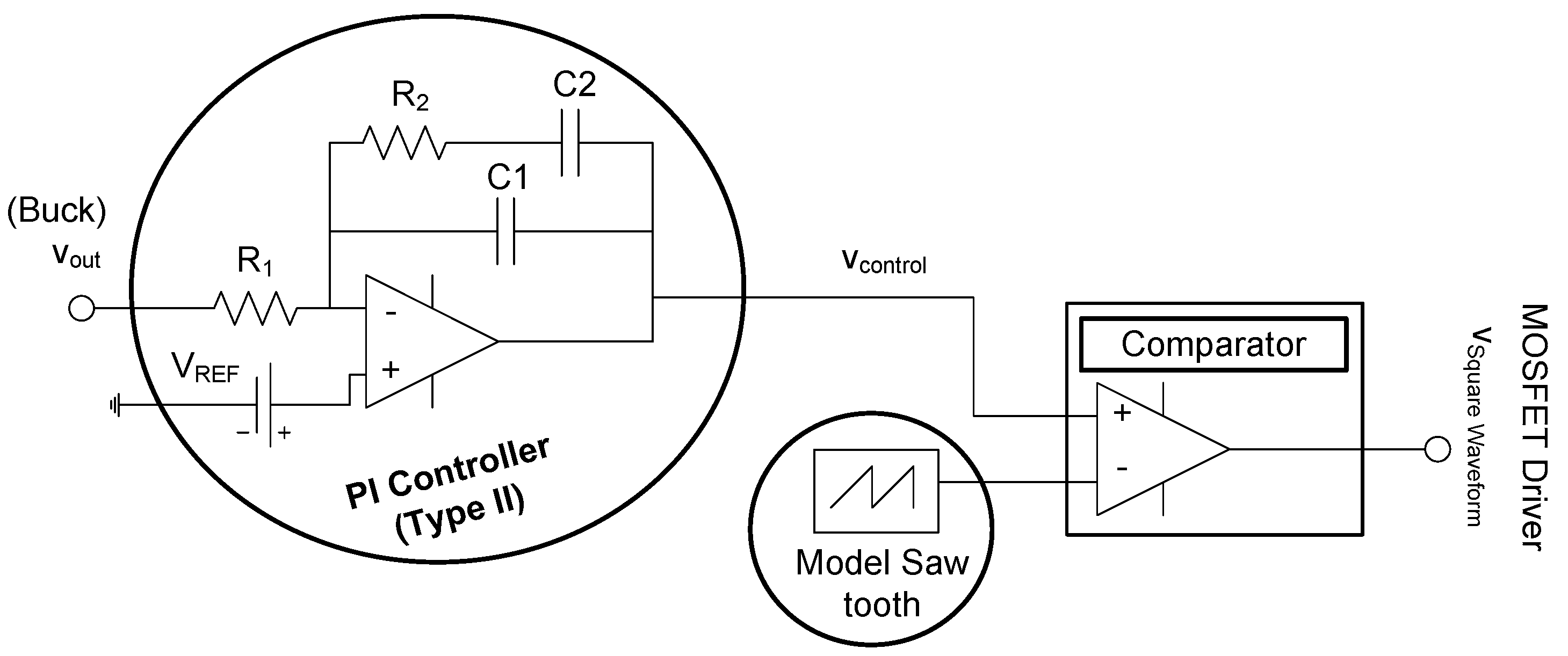
At first, it is important to analyze the control circuit (
Figure 3).
As it can be seen in
Figure 3, the control circuit is composed of three fundamental elements: the PI controller, the Comparator, and the Saw-Tooth Generator.
The first two elements will be integrated into the main function (fourth module). Therefore, the second module is only responsible for generating the saw-tooth signal, which is responsible for defining the converter operating frequency.
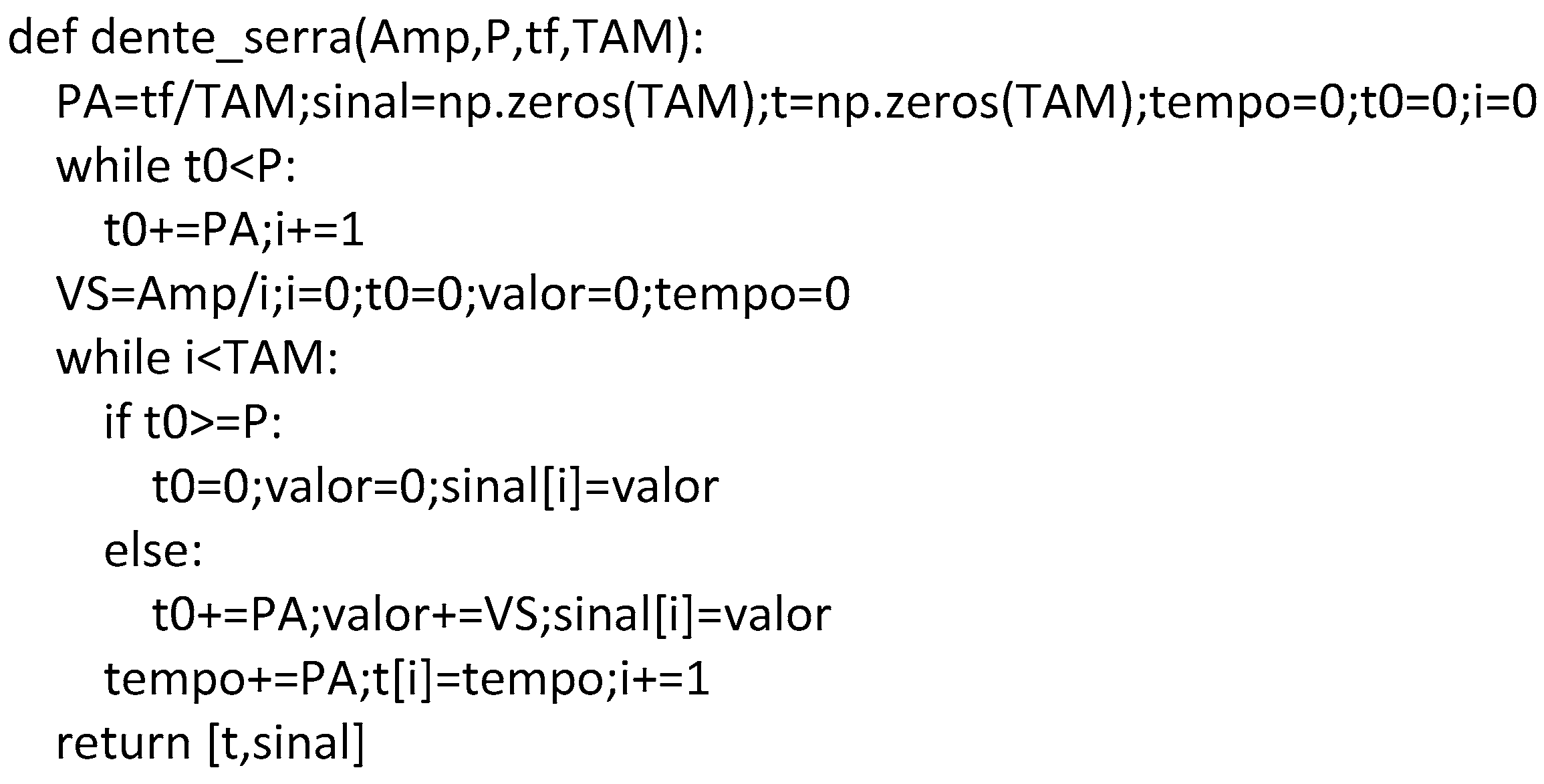
The saw-tooth generator must be implemented in a specific function (
Figure 4). The function should receive as input arguments the amplitude of the Saw-tooth waveform (Amp), the Period (P), the final simulation time (t
f), and the total number of iterations, TAM. In turn, the function returns the time vector (t), as well as a saw-tooth waveform with period P (sinal).
2.3. Fourth Module
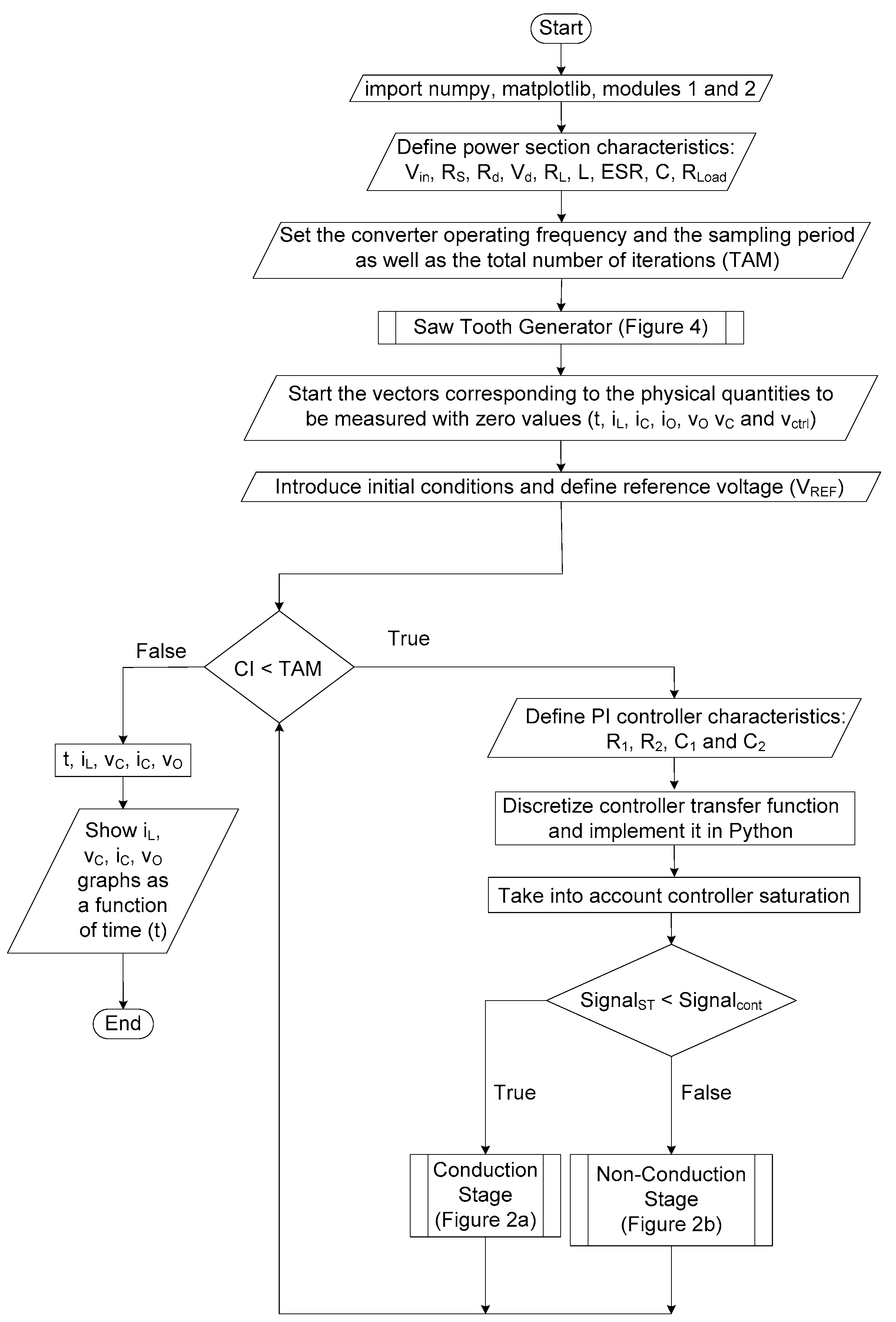
The fourth module corresponds to the main function, which must properly integrate the previous modules and, simultaneously, implement the PI controller and the comparator.
Figure 5 presents a flowchart that shows how to implement the main function in Python.
CI represents the current iteration, and t, iL, vC, vO, iC, SignalST and Signalcont represent the vectors referring to the following quantities: the time, inductor current, output voltage component due exclusively to C, output voltage, capacitor current, saw-tooth signal and PI controller output (vcontrol), respectively.
3. Buck Converter Design
In this section, the process of designing a buck converter will be presented. At first, the power section will be designed using the following specifications.
Table 1 shows that the converter must operate in CCM, that is, the L
ps inductance (L) must be greater than its critical value (L
critical). In order to compute L
critical, it is necessary to perform the following steps:
First, a set of rules must be considered, namely, the converter must be operating in a steady-state regime, the inductor average voltage must be zero, the average current in the capacitor should also be zero, all components should be considered ideal, and the capacitor capacitance should be large enough.
Following this, after analyzing the theoretical waveform of the inductor current, it is possible to obtain the mathematical relationship between the inductor ripple current and the input and output voltage.
Finally, we should consider the following condition: the average value of the inductor current is equal to half of its ripple (critical conduction mode or transition mode); it is possible to calculate the Lcritical as shown in (1).
Taking into account condition (1), an inductor with an inductance of 22 μH (11 A) was chosen. In order to reduce the output voltage ripple, an aluminum electrolytic capacitor (Al-Cap) was used, as it has a high capacitance value. Therefore, an Al-Cap with 1000 μF (25 V) capacitance was chosen.
The converter output voltage ripple is essentially due to the capacitor ESR, because its operating frequency is close to the capacitor resonance frequency [
20]. The Al-cap mathematical model is composed of a series connection of a resistor (ESR), an inductor (ESL), and a capacitor (C). When the Al-cap operates near its resonant frequency, the ESL effect cancels the C effect. Thus, using the method proposed in [
21], it is possible to obtain the capacitor ESR experimentally (ESR = 0.077 Ω).
Following this, the converter control section will be designed. For this purpose, the specifications presented in
Table 2 will be applied.
In order to design the controller, it is necessary to obtain a mathematical model that represents the dynamic behavior of the system to be controlled (dynamic model). The dynamic model can be represented through state space representation or through the transfer function. The first one can be obtained through a set of differential equations that model the system, and the second one (transfer function) can be obtained through state space representation (first one). From the controller’s point of view, its input signal corresponds to the converter output voltage, and its output is the control signal (duty cycle). For this reason, the buck converter transfer Equation (2) relates the output voltage (v
o) of the converter with the duty cycle (d).
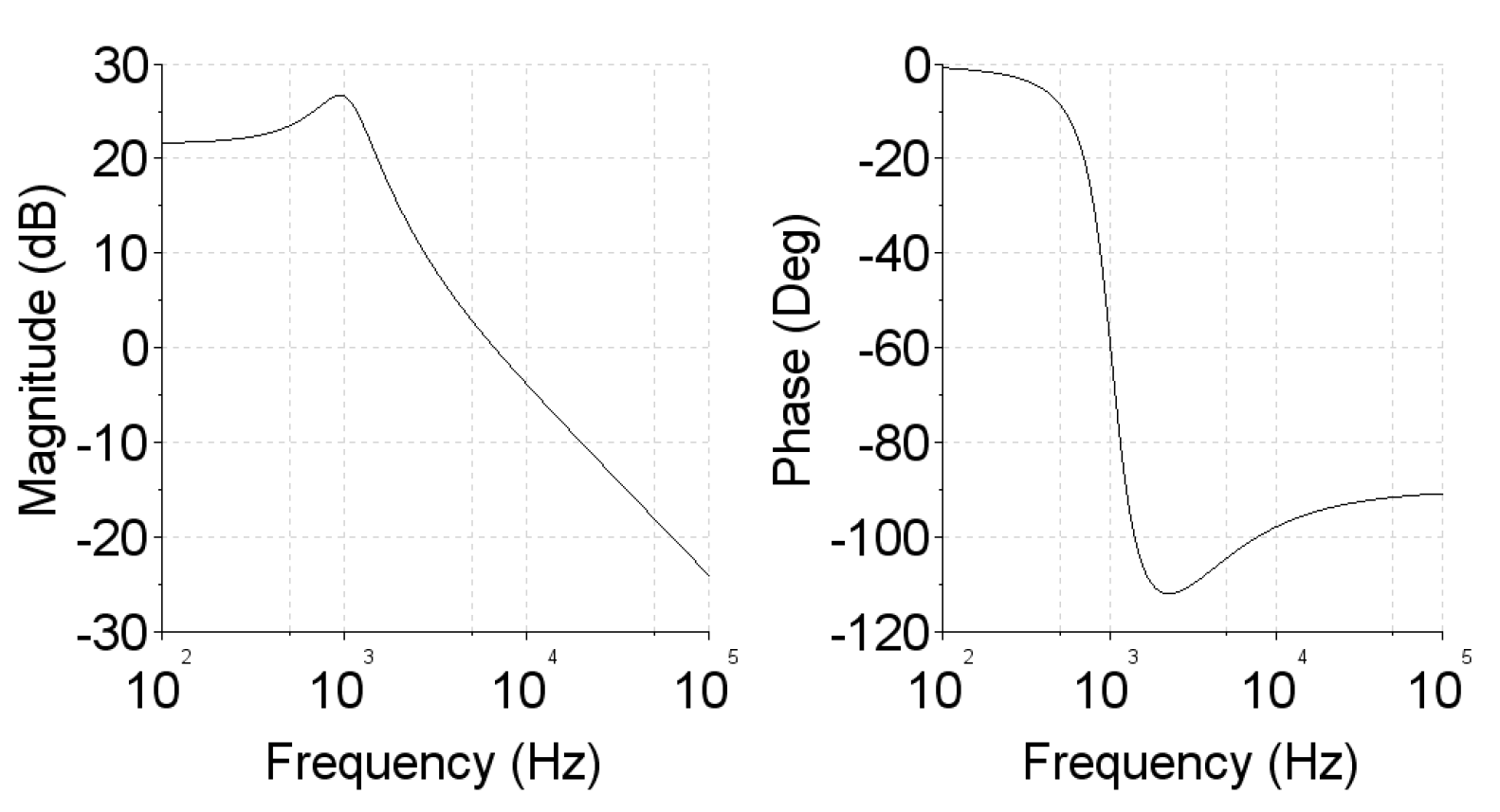
The effect of the complex conjugate poles of transfer Equation (2) will cause the gain curve to drop −40 db, and tries to bring the phase curve towards −180°. A few frequencies later, the zero effect resulting from the ESR arises, that is, there is a reduction in the slope of the gain curve to −20 db, and the phase curve shifts to −90° (
Figure 6).
In the controller design (Type II), the k-factor method will be used. The type II controller provides a region between its zero (w
Z) and its pole (w
P), in which the gain value is constant and the phase undergoes a shift from −90° to (φ
boost−90°). Therefore, it is possible to introduce the desired phase margin (PM
desired) at the crossover frequency (f
C) of the system (buck converter plus the controller) if w
Z and w
P are properly chosen. The k-factor method computes the w
Z, w
P and gain (K
C) values that ensure the initial specifications (
Table 2).
Following this, the k-factor method will be applied. At first, it is necessary to obtain the phase of the buck converter (2) at the crossover frequency (
Figure 6).
From the previous figure, it is possible to obtain the phase of plant (2) at fC (φsystem ≈ −104.5°).
The required phase boost, φ
boost, can be computed as follows [
22]:
Using the computed φ
boost, it is possible to obtain the controller w
P and w
Z as follows [
22]:
Equation (4) introduces a φ
boost shift at the geometric mean of w
Z and w
P, which is w
C. The controller transfer function (
Figure 3) can be represented by the following equation:
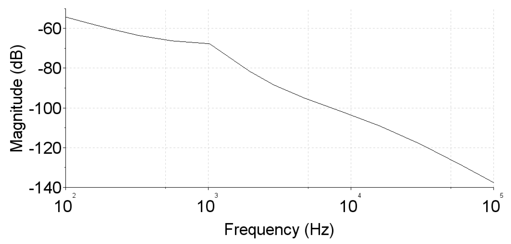
In order to compute KC, it is necessary to represent the Bode magnitude plot of the set of the controller (KC = 1), modulator and buck converter.
The value of K
C is equal to the inverse of the magnitude value of the graph of
Figure 7 at the crossover frequency (−95.74 db).
Finally, the controller transfer function is obtained.
The following
Figure 8 represents the frequency response of the set of the controller (K
C = 61 k), modulator and buck converter.
The previous figure shows that the final system behaves according to the following specifications (
Table 2): PM
desired = 180° − (final system phase at f
C) = 45°.
Alternatively, it is possible to obtain the following transfer function for the PI controller (type II) represented in
Figure 3.
Using (5) and (8), it is possible to write the following:
Assuming R2 = 1 kΩ, it is possible to calculate the remaining controller elements: C2 ≅ 117 nF, R1 ≅ 129 Ω and C1 ≅ 9.4 nF. In this way, the following standard values were chosen: R1 = 100 Ω, R2 = 1 kΩ, C1 = 10 nF and C2 = 100 nF.
4. Proposed Tool versus LTspice
In this section, a comparison will be performed between the proposed tool and the LTspice simulator.
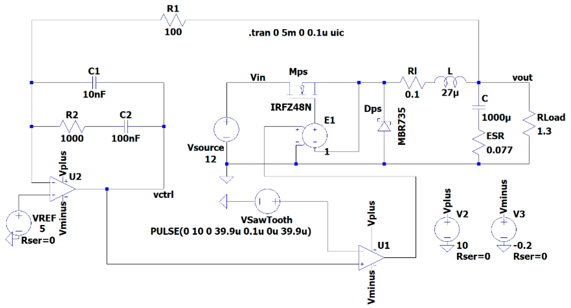
Figure 9 shows the implementation of the converter in LTspice.
It is important to mention that LTspice is one of the most frequently used pieces of simulation software in both industry and academia [
23,
24,
25]. However, LTspice does not allow the implementation of FDT; for that reason, the third module will be presented in
Section 5.
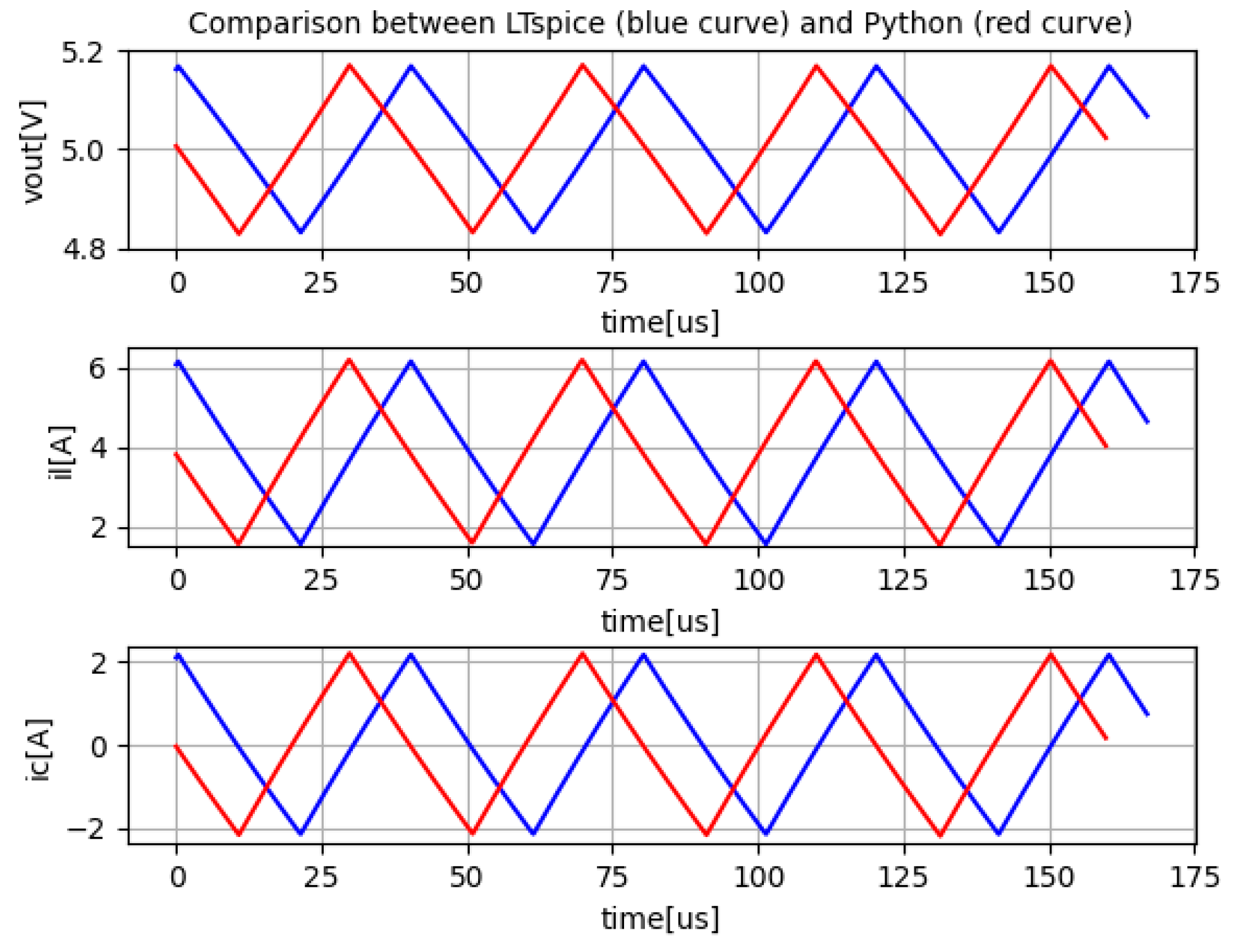
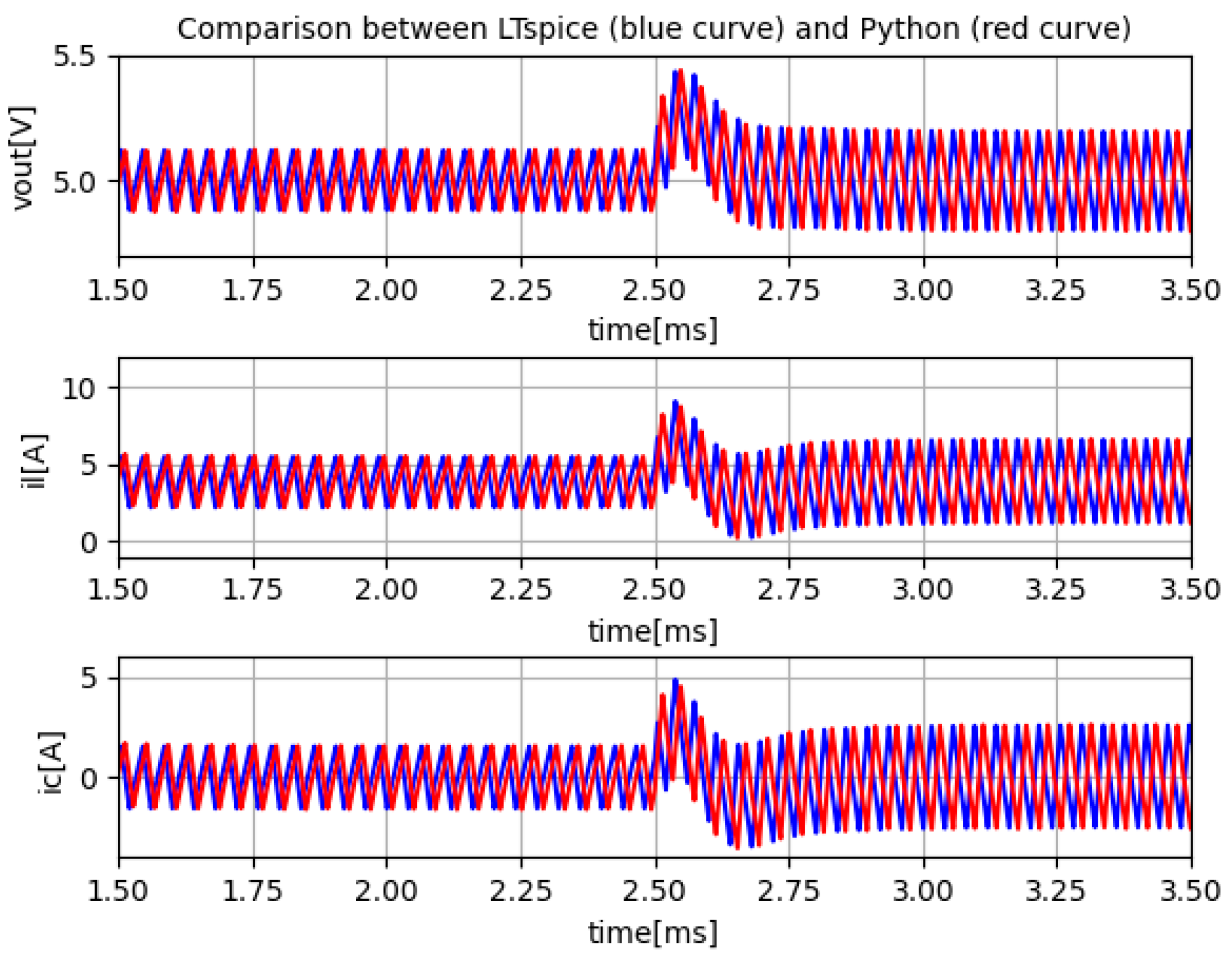
In order to assess the feasibility of the proposed tool, three different operating conditions are considered: steady state (
Figure 10), load variation (
Figure 11) and input voltage variation (
Figure 12).
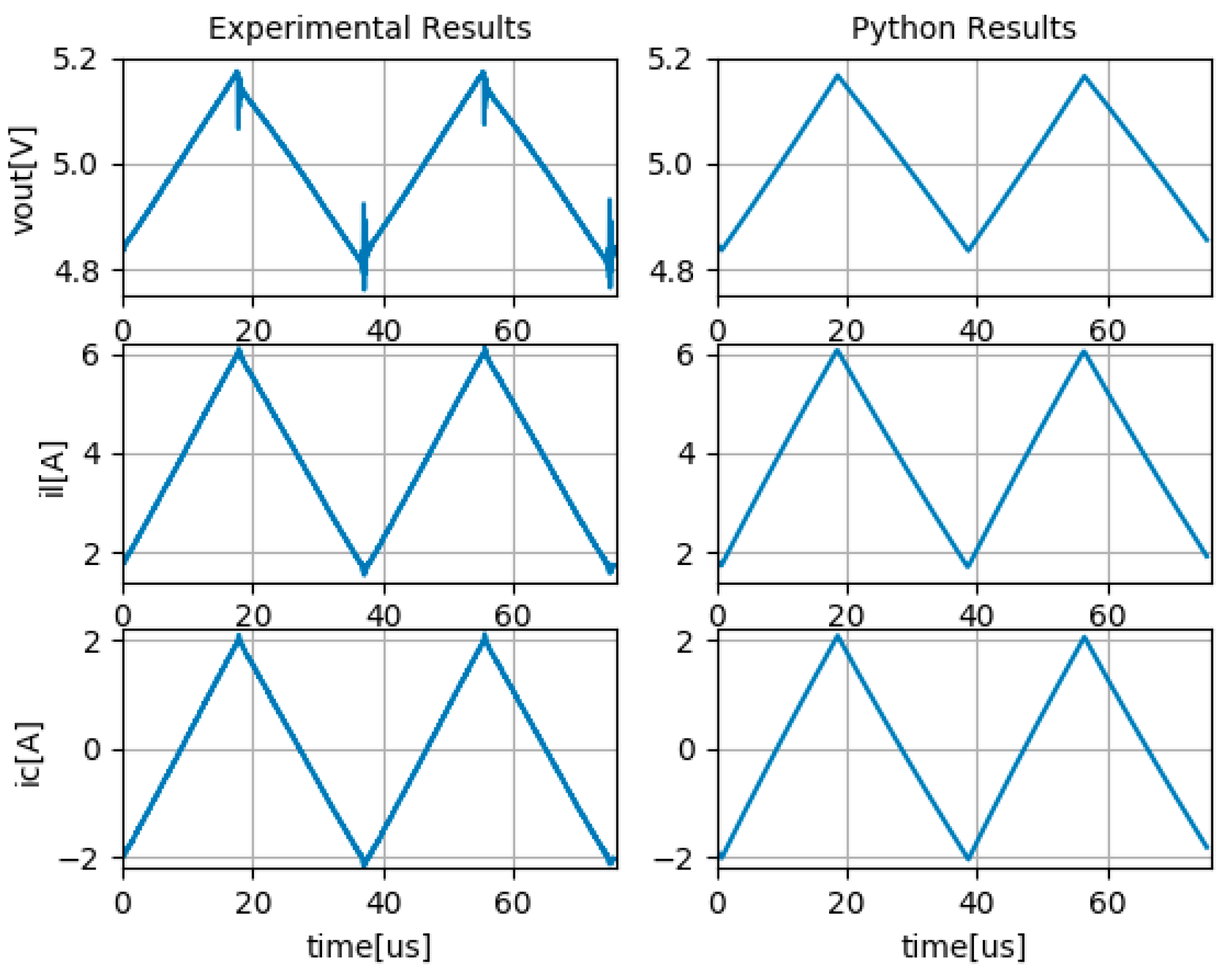
The previous graphs show that the proposed tool presents very similar results to LTspice regarding the quantities under analysis (output voltage—vO, inductor current—iL, and capacitor current—iC) for the different operating conditions (steady state, load variation and input voltage variation).
The Lps inductance value of the experimental prototype was experimentally calculated (27 µH). For this reason, a 27 µH value was used in the simulations instead of 22 µH.
5. Fault Diagnostics Technique—Third Module
This paper does not intend to present a new fault diagnostics technique for DC-DC converters; rather, it presents a tool that can be very useful in its development. However, it is important to introduce the issue of fault diagnosis such that the relevance of the proposed tool can be understood.
About 30% of converter failures are caused by capacitor degradation [
26], which makes this component one of its most vulnerable elements [
8,
9,
26]. In the literature, several fault diagnostic methods are proposed that allow the evaluation of the health condition of capacitors used in DC-DC converters [
8,
9,
27,
28,
29,
30,
31,
32,
33].
During the aging process, Al-Caps lose part of their electrolytes, which results in an increase in the ESR. Therefore, it can be concluded that the identification of this electrical parameter allows the assessment of Al-Cap health status. The estimation of the ESR will be performed by computing the capacitor impedance at the converter switching frequency (csf), as the converter operates very close to the capacitor’s resonant frequency [
33].
The calculation of the capacitor impedance is carried out by computing the ratio between the first harmonic (h
csf) of the capacitor voltage (h
csfv
C) and current (h
csfi
C) [
33]. In order to compute the h
csf value of the capacitor voltage and current, an FFT algorithm will be used. The NumPy library provides a function that computes the fft of a signal, which was used in the development of the third module.
The third module is composed of a function that receives as input arguments t, vO and iC. The above signals must have a duration of the converter switching period (csp), and must be properly handled such that the NumPy fft function can correctly compute the hcsf of both signals. Following this, the ESR is calculated by computing the ratio between hcsfvC and hcsfiC. Finally, the function returns the ESR value.
Module 3 can be easily integrated into the algorithm of
Figure 5. At first, it is necessary to obtain the input arguments of the function: t, v
O and i
C. Therefore, for each csp, the three vectors must be obtained. As a result, the function will return the ESR value for that specific csp.
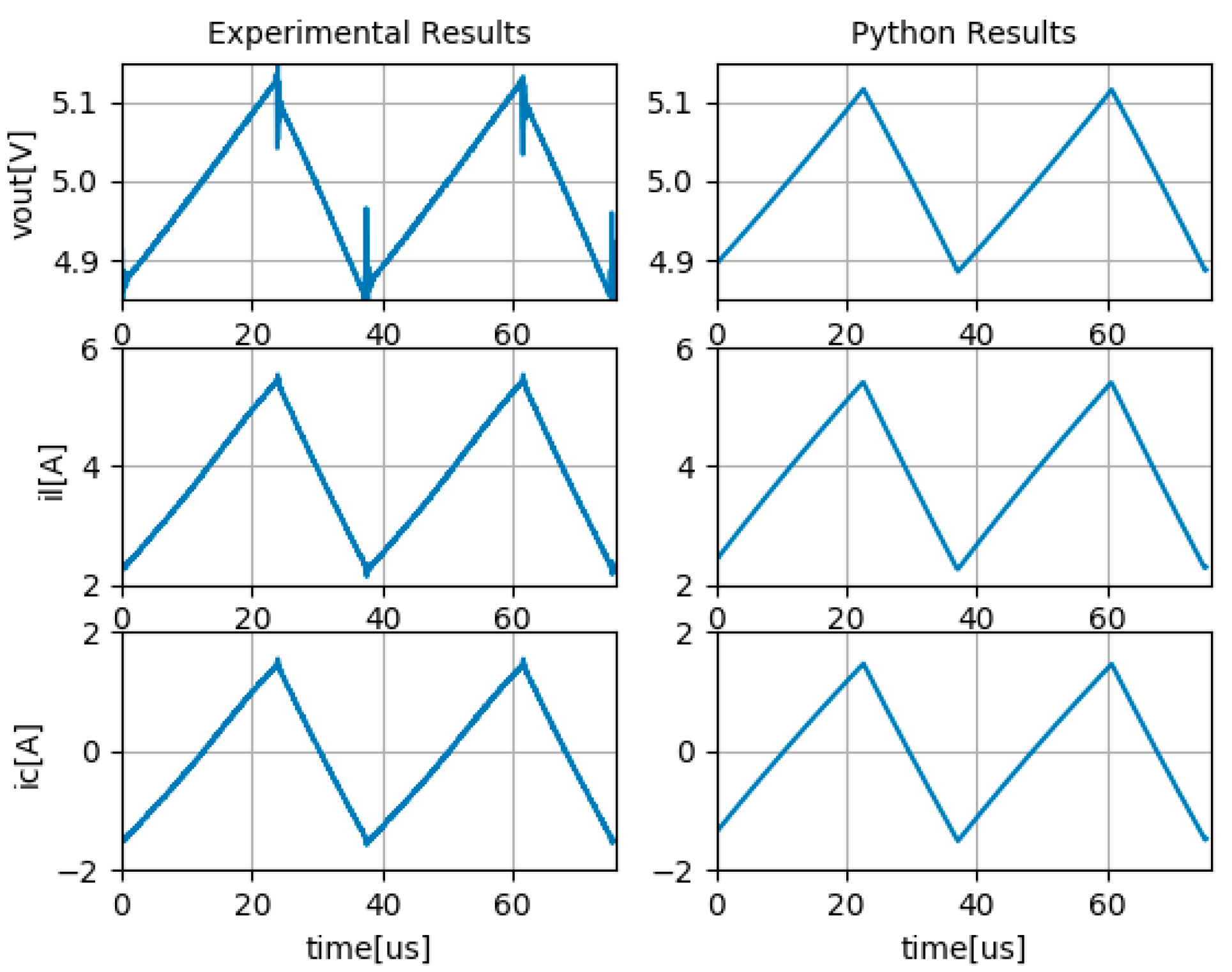
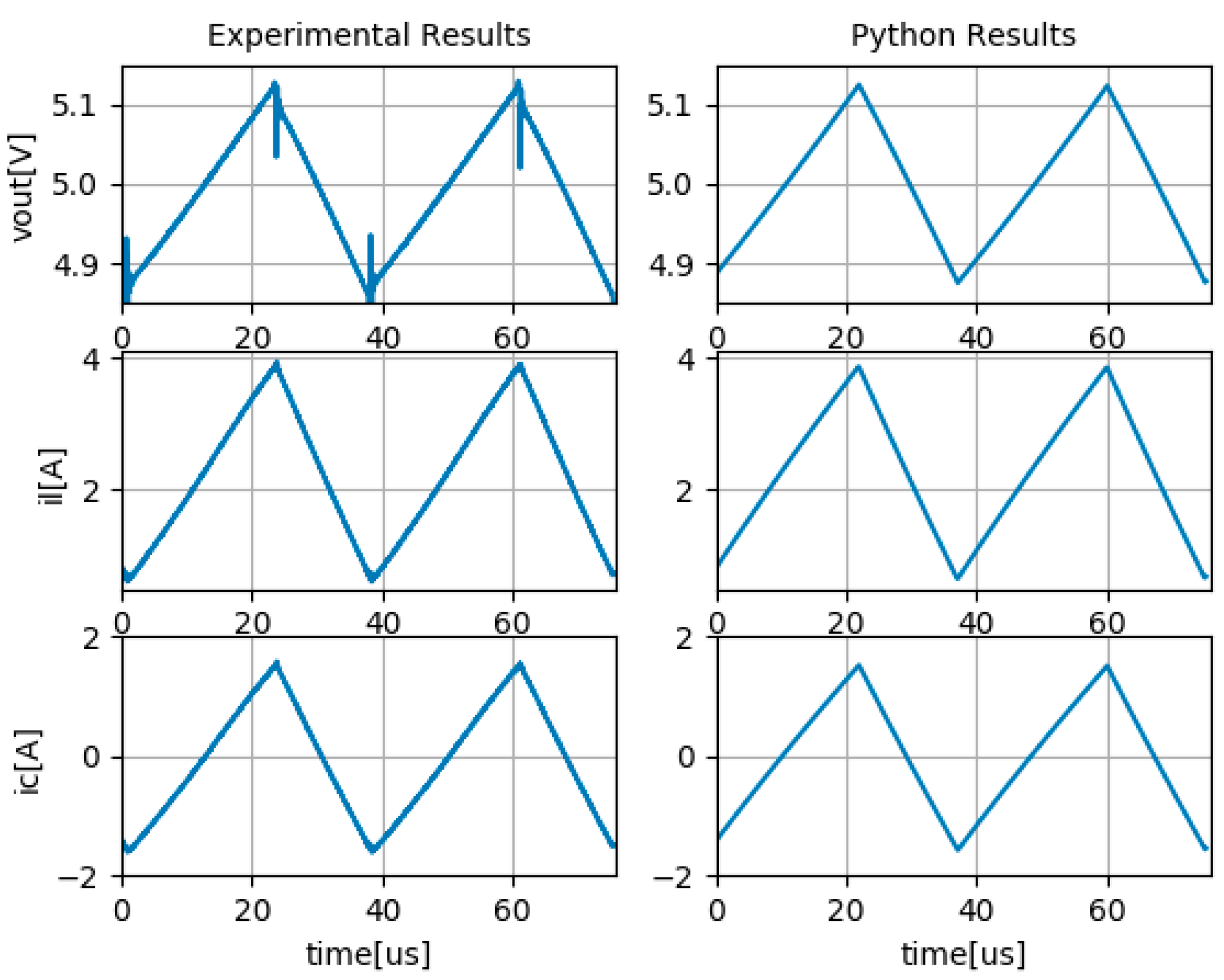
In order to evaluate the applicability of the third module, four different operating conditions will be considered, which are summarized in
Table 3.
Figure 13,
Figure 14,
Figure 15 and
Figure 16 show the v
O, i
L and i
C waveforms for the four situations represented in
Table 3. From these figures, it is possible to compare the waveforms obtained from the proposed tool with the experimental ones. The experimental results were obtained from an experimental prototype with characteristics similar to the circuit of
Figure 9 (considering the operating conditions in
Table 3).
The previous figures contain data for two csp, such that by using module 3 it is possible to estimate the ESR value for two csp.
At first, module 3 was applied to the simulation results (Python results—proposed tool). Thus, considering the four situations described in
Table 3, the maximum error obtained was less than 0.35% (ESR = 0.077265 Ω).
Next, module 3 was applied to the experimental waveforms. As a result, the following ESR values were obtained (
Table 4).
The previous results (ESR estimation from the experimental and simulation results) clearly show that the proposed tool can be very useful. Thus, at first, it is possible—with a high degree of certainty and using the proposed tool—to predict the reliability of an FDT. It should be noted that, in this first step (ESR estimation from simulation results), it is not necessary to design an experimental prototype.
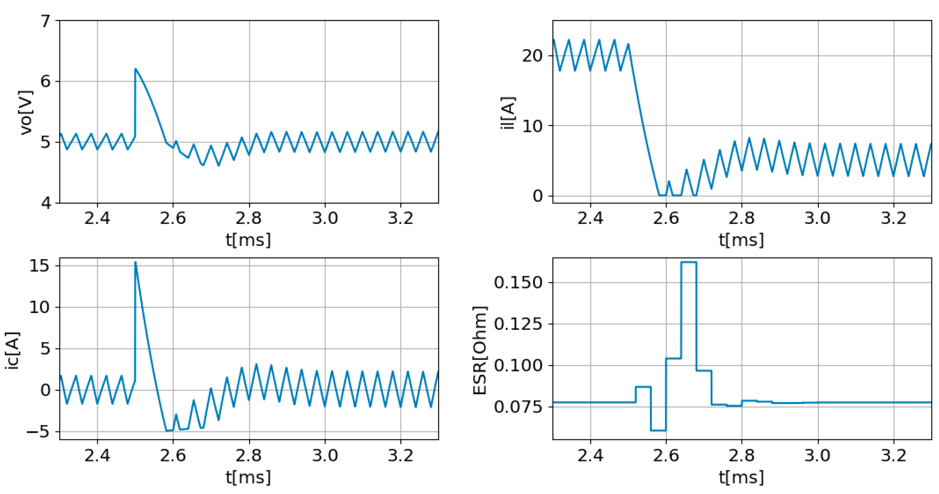
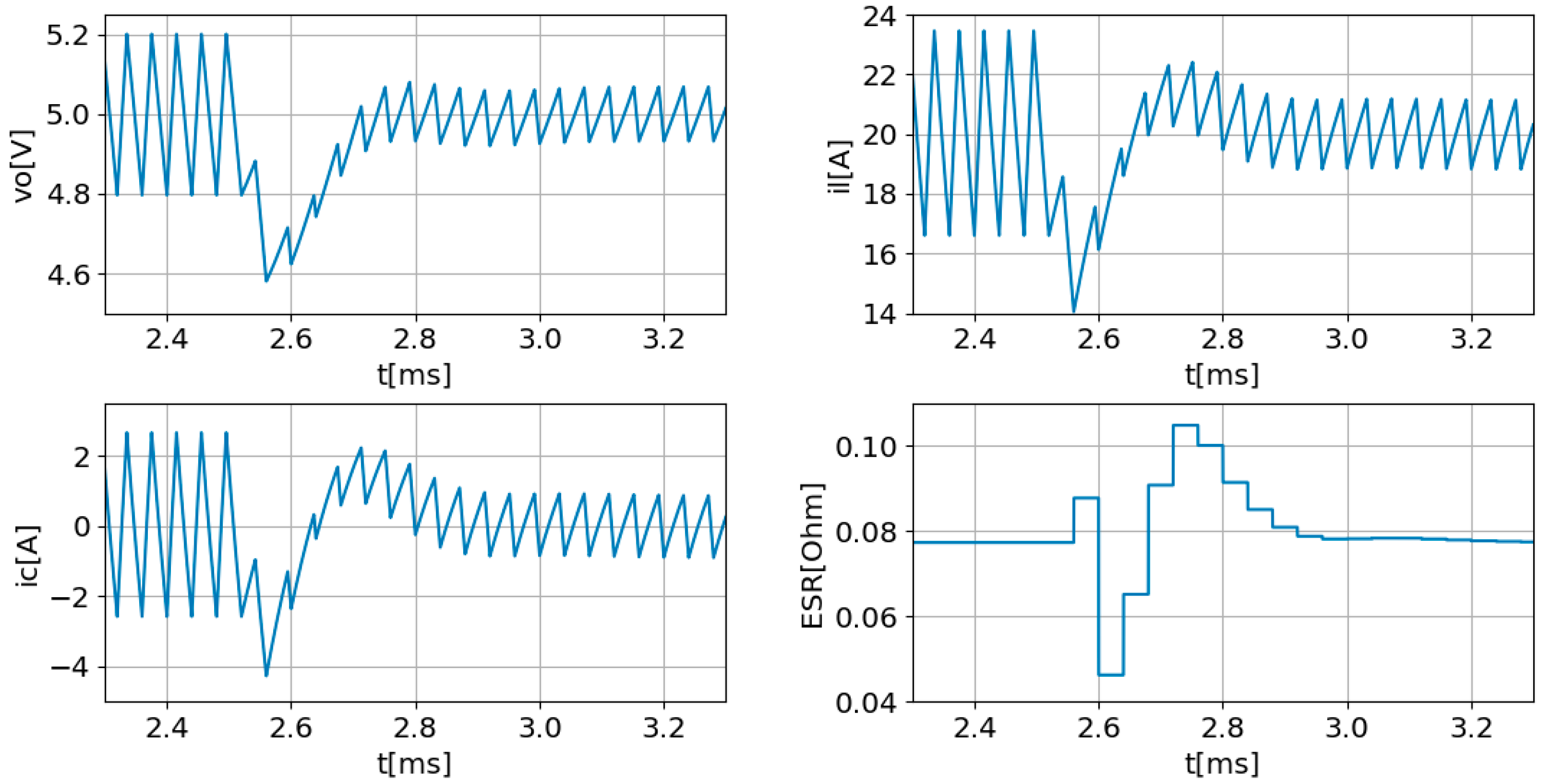
The relevance of the proposed tool becomes even more evident when the system is subjected to external disturbances such as load variation or input voltage variation. The proposed tool can easily evaluate the performance of an FDT during transients, as shown in
Figure 17 and
Figure 18.
Figure 17 shows the response of the FDT when the converter is subjected to a load variation (from 20 A to 5 A at 2.5 ms).
The previous figure shows that during the transient, the maximum error was greater than 110%.
Figure 18 shows the response of the FDT when the converter is subjected to an input voltage variation (from 19 V to 9 V at 2.5 ms).
The previous figure shows that during the transient, the maximum error was greater than 40%.
In order to understand the meaning of previous errors in the context of an FDT, it is important to delve deeper into the issue of Al-Caps failures.
The Al-Caps present two types of failures: catastrophic and parametric failures. The catastrophic failures lead to the destruction of the component through a short or an open circuit. Thus, the capacitor completely loses its function. In the parametric failure, the capacitor does not completely lose its function; however, its electrical characteristics deteriorate (the ESR increases). Usually, capacitor manufacturers define the end life limit of Al-Caps as being when the ESR doubles with respect to its initial value [
8]. The previous threshold defines a significant increase in the occurrence of a catastrophic failure.
In this way, using the proposed tool, it was possible to conclude that the analyzed FDT can lead to an error in assessing the health status of the Al-Caps during the transient regime. This situation is particularly serious in critical applications, which is why a much more conservative threshold is defined for the ESR [
8].
6. Conclusions
This paper presented a tool that simulates the operation of a closed-loop SMNI DC-DC converter and, simultaneously, implemented an FDT in real time.
The proposed solution was implemented in Python, as it is a high-level open-source programming language oriented to numerical analysis, unlike MATLAB/Simulink, which is a proprietary language, and is for that reason much less flexible. In this particular, it is important to mention that proprietary languages makes the implementation of FDT much more difficult. By comparing the proposed tool with LTspice and experimental results, it was possible to prove its applicability. Therefore, it was demonstrated that the proposed tool allows the evaluation of the reliability of FDTs for SMNI DC-DC converters at different operating conditions. In this regard, it is important to highlight one of the great advantages of the proposed tool: it allows us to easily verify the deficiencies of the FDT without having to design an experimental prototype. Another important aspect of the proposed tool is the fact that it allows the evaluation of the applicability of the FDT in real time. In the case of the analyzed FDT, the estimated ESR value corresponds to the previous csp, which is in the order of the tens of μs. Therefore, it is possible do conclude that the system responds in real time.
The paper also presented an algorithm that can be very useful in the design of buck converters.


